Group
1. Compare the performance and development workflows for other architectures
Individual
1. Read a microcontroller data sheet
2. Program your board to do something, with as many different programming languages and programming environments as possible
Plan for the week
In previous weeks, we did electronics production where we knew how to make the boards by milling, stuffing elctronics component with solder followed by designing the circuit by using CAD like eagle and tested it. Microcontroller is like an empty glass unless something is pushed inside it. In order to operate microcontroller as per our expectatiom, we have to push some logic inside the microcontroller based on which it operates. So that logic is attained by doing programming in differnt platformslike arduino IDE, Embedded C, Atmel studio etc. These platforms let us input in understandable language and finally to hex code that machine understand

Microcontroller
A microcontroller is an integrated circuit (IC) which is small, low cost and self contained computer designed to handle a specific task in embedded systems. In simple words, a microcontroller (MCU or Microcontroller Unit) is a small computer integrated in to a single chip. We can also explain it as programmable silicon chip which is clock driven, register based, accepts input and provides output after processing it as per the instructions stored in the memory.
A computer is a general purpose device which we can use for word processing, watching movies, editing videos, web browsing, developing softwares etc. While a microcontroller is intended to do some specific tasks like controlling a washing machine, controlling an air conditioning etc.
Microcontroller consists of Arithmetical and Logical Unit (ALU), Control Unit and Register Array. As the name indicates ALU performs all arithmetic and logical operations on the data received from input devices or memory. Register array consists of a series of registers like accumulator (A), B, C, D etc. which acts as temporary fast access memory locations for processing data. As the name indicates, control unit controls the flow of instructions and data throughout the system. So basically a microprocessor takes input from input devices, process it as per instructions given in the memory and produces output.
Attiny24/44/84 datasheet
You don’t have to understand everything in a datasheet. There’s a lot of information that might not be of any use to you. There are some important parts of the datasheet that you should pay particular attention. You can find datasheet of every electronic component in a pdf format. The datasheet of ATTiny 24/44/84 can be downloaded from this link.
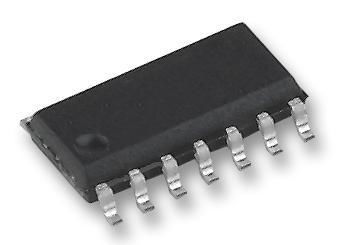
Pin descriptions
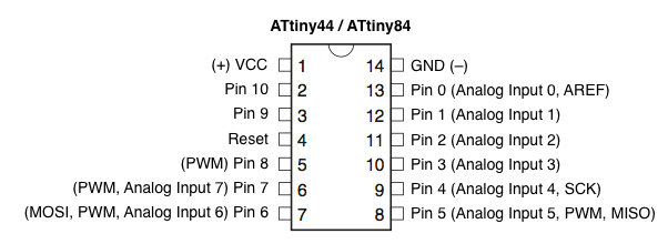
For arduino
Block diagram
ATtiny24/44/84 is a low-power CMOS 8-bit microcontroller based on the AVR enhanced RISC architecture. By executing powerful instructions in a single clock cycle, the ATtiny24/44/84 achieves throughputs approaching 1 MIPS per MHz allowing the system designer to optimize power consumption versus processing speed.
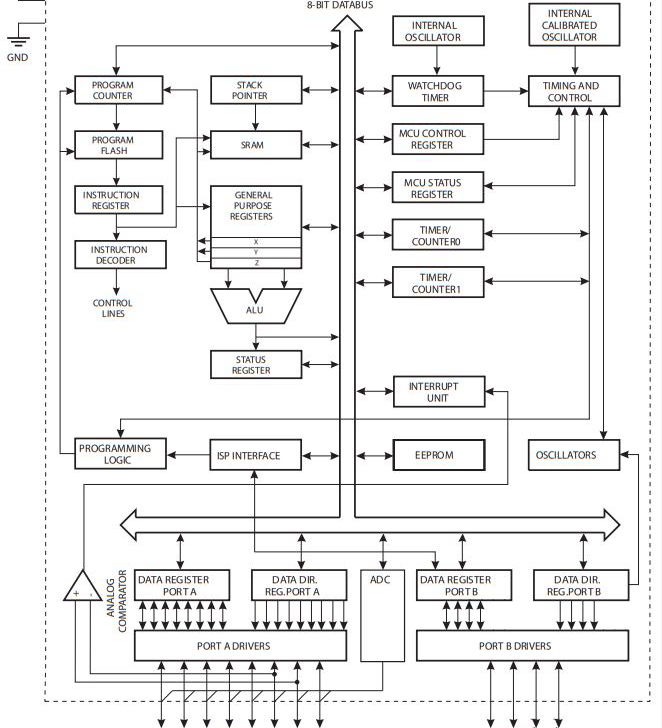
The AVR core combines a rich instruction set with 32 general purpose working registers. All 32 registers are directly connected to the Arithmetic Logic Unit (ALU), allowing two independent registers to be accessed in one single instruction executed in one clock cycle. The resulting architecture is more code efficient while achieving throughputs up to ten times faster than conventional CISC microcontrollers.
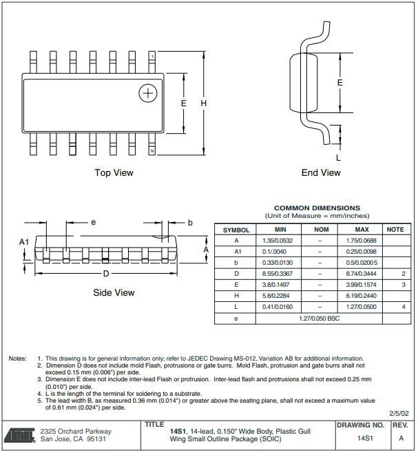
Physical Dimension
Schematics from Electronics Design week
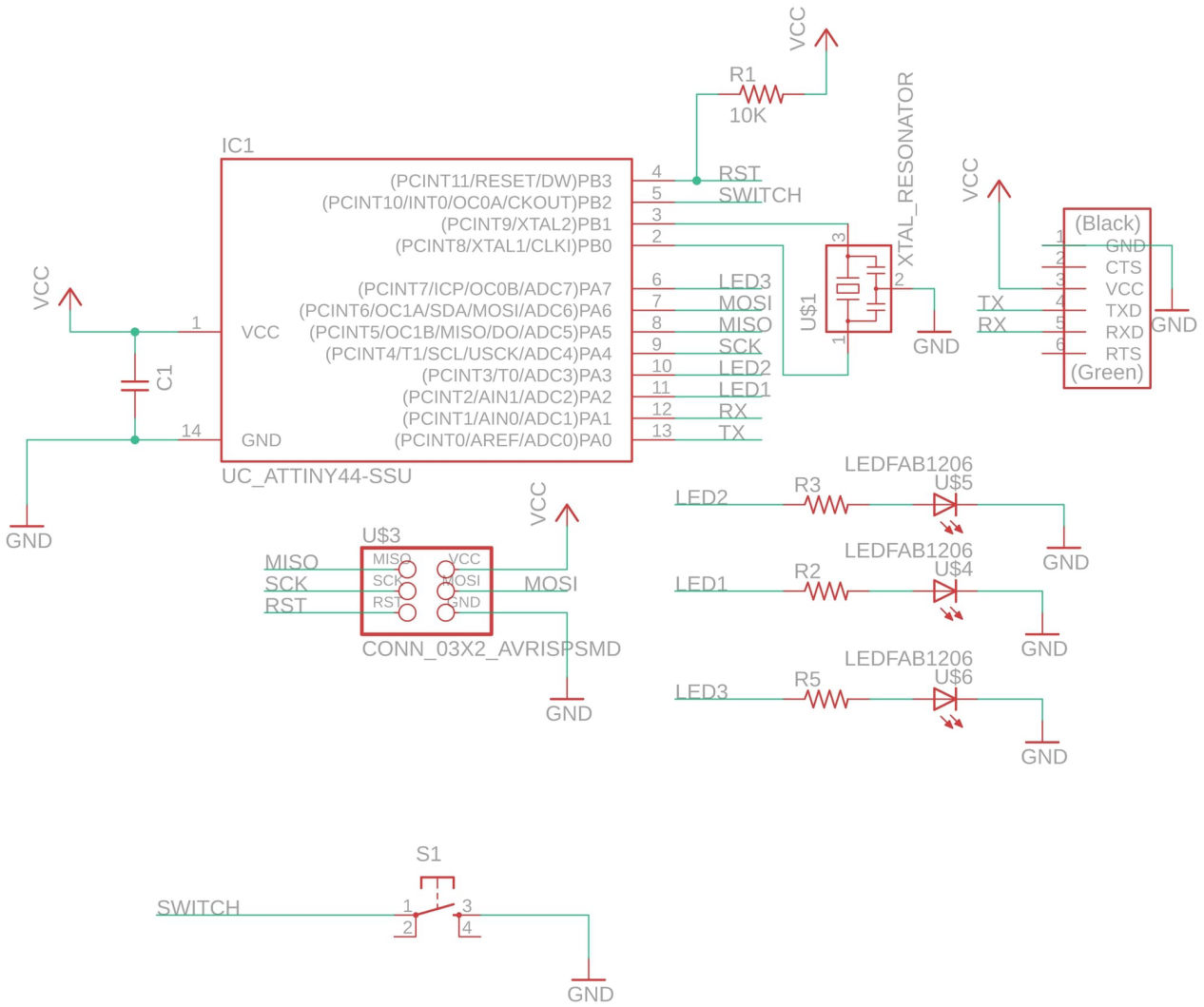
We will be using these for applying the embedded programmin gon the microcontroller. We will be taking PB2 for input and PA2, PA3 and PA7 as an output.
Arduino IDE
Arduino is an open-source electronics platform based on easy-to-use hardware and software. It's intended for anyone making interactive projects. Download the Arduino IDE software from this link. Now that the software is downloaded install and open the software and follow the steps below
1. Open preferences
file >> preferences
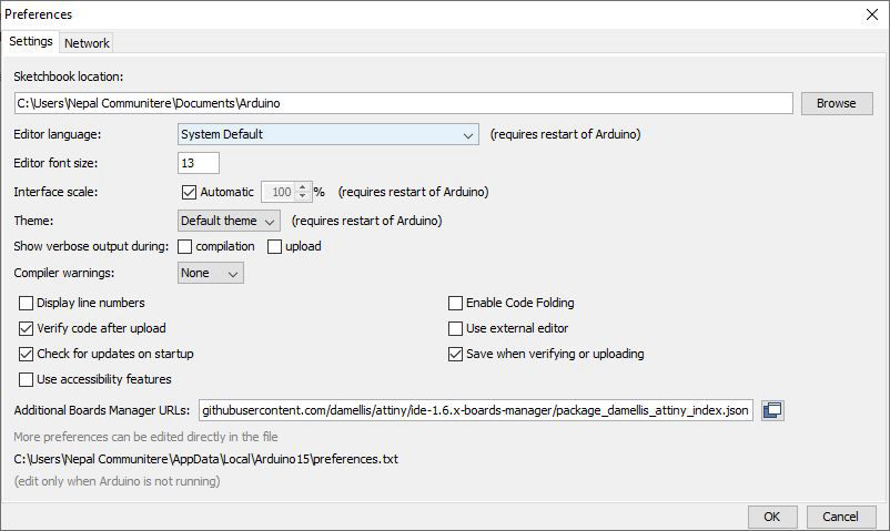
2. Copy the following link in the Additional boards manager
https://raw.githubusercontent.com/damellis/attiny/ide-1.6.x-boards-manager/package_damellis_attiny_index.json
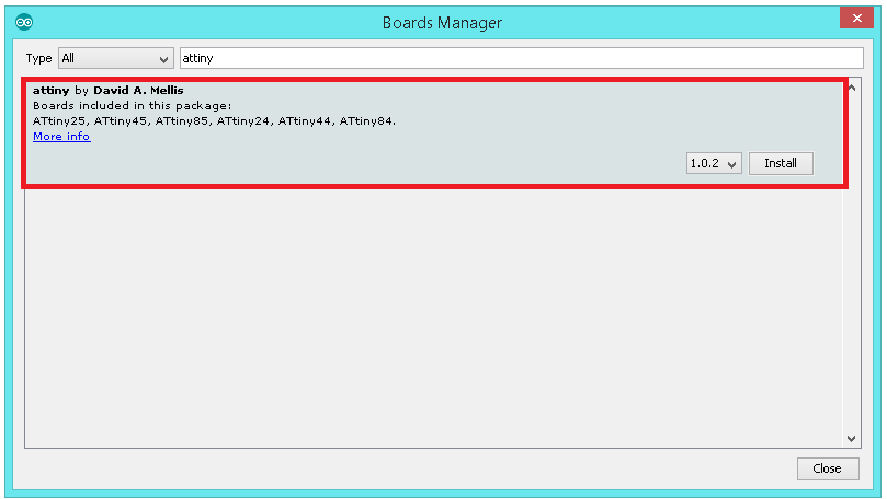
3. After adding the URL open Board Manager by clicking
Tools >> Board >> Board Manager
Search for ATTiny and install the board.
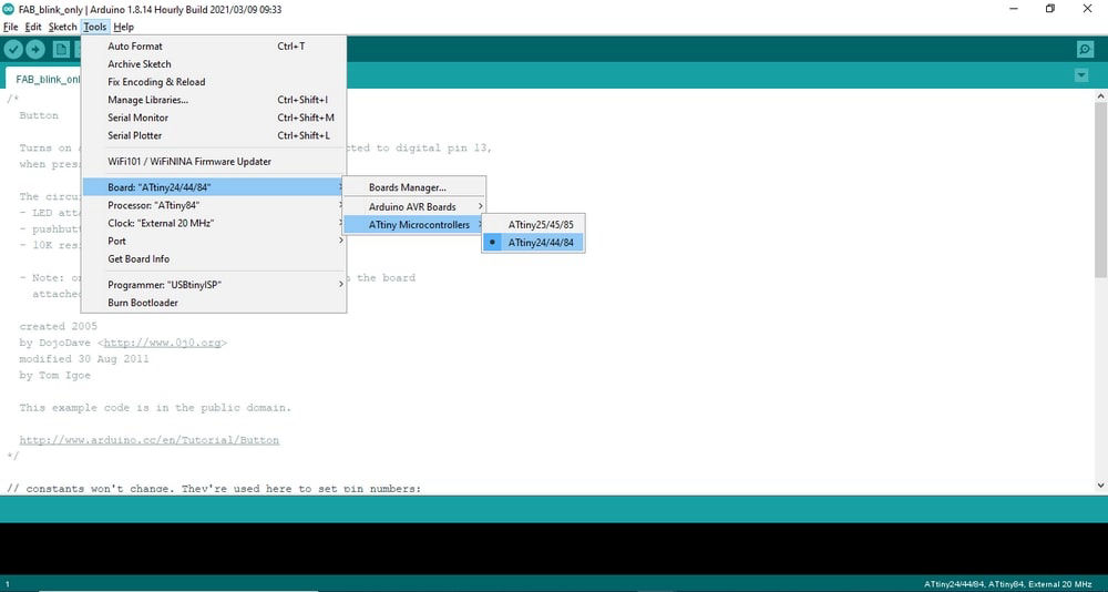
4. Select
Board : ATTiny microcontrollers >> ATTiny 24/44/84
Processor : ATTiny 84
Clock: External 20MHz
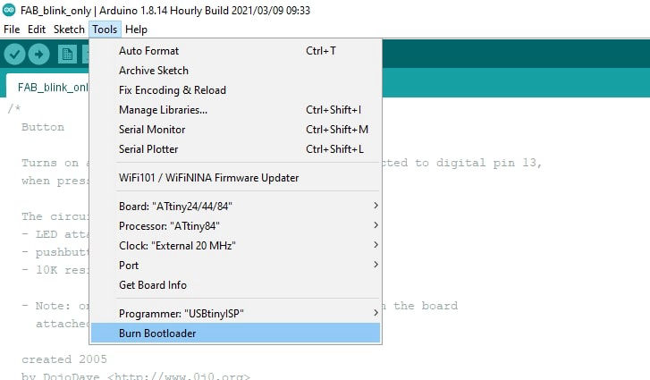
5. Now click on bootloader. What bootloader does is it sets up the conditions for your board like frequency which is the reference for time. Whether the clock is external or internal etc
Tools >> Bootloader
// constants won't change. They're used here to set pin numbers:
const int ledPin1 = 3;
const int ledPin2 = 2;
const int ledPin3 = 7;
// variables will change:
int buttonState = 1; // variable for reading the pushbutton status
void setup() {
// initialize the LED pin as an output:
pinMode(ledPin1, OUTPUT);
pinMode(ledPin2, OUTPUT);
pinMode(ledPin3, OUTPUT);
}
void loop() {
// turn LED on:
digitalWrite(ledPin1, HIGH);
delay (10);
digitalWrite(ledPin1, LOW);
delay (10);
digitalWrite(ledPin3, HIGH);
delay (10);
digitalWrite(ledPin3, LOW);
delay (10);
digitalWrite(ledPin2, HIGH);
delay (10);
digitalWrite(ledPin2, LOW);
delay (10);
}
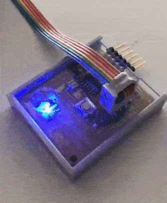
Here I tried blinking it only which you can see above
Then I tried programming fot blinking it only when switch is pressed which you can see below
// constants won't change. They're used here to set pin numbers:
const int buttonPin = 8; // the number of the pushbutton pin
const int ledPin1 = 3;
const int ledPin2 = 2;
const int ledPin3 = 7;
// variables will change:
int buttonState = 1; // variable for reading the pushbutton status
void setup() {
// initialize the LED pin as an output:
pinMode(ledPin1, OUTPUT);
pinMode(ledPin2, OUTPUT);
pinMode(ledPin3, OUTPUT);
// initialize the pushbutton pin as an input:
pinMode(buttonPin, INPUT_PULLUP);
}
void loop() {
// read the state of the pushbutton value:
buttonState = digitalRead(buttonPin);
// check if the pushbutton is pressed. If it is, the buttonState is HIGH:
if (buttonState == LOW) {
// turn LED on:
digitalWrite(ledPin1, HIGH);
delay (200);
digitalWrite(ledPin1, LOW);
delay (200);
digitalWrite(ledPin3, HIGH);
delay (200);
digitalWrite(ledPin3, LOW);
delay (200);
digitalWrite(ledPin2,
HIGH);
delay (200);
digitalWrite(ledPin2, LOW);
delay (200);
} else {
// turn LED off:
digitalWrite(ledPin1, LOW);
digitalWrite(ledPin2, LOW);
digitalWrite(ledPin3, LOW);
}
}
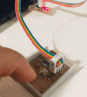
After program is written, it was compile and pushed to the board via the ISP we made in 4th week. You can see the video below.

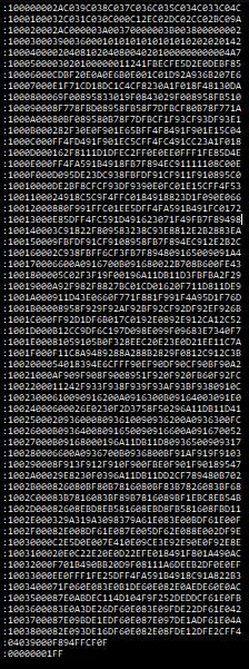
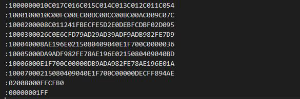
Hex code generated is as below which is sent to the processor. This is very long as arduino IDE is comparatively high language than embedded c or assembly language
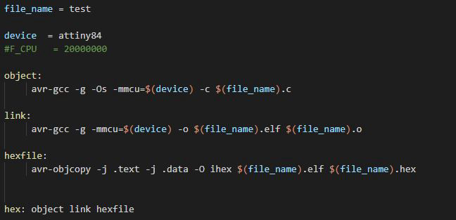
AVR GCC
AVR-GCC is a compiler that takes C language high level code and creates a binary source which can be uploaded into an AVR micro controller. Thus AVR-GCC might be regarded as a 'C' cross compiler for producing AVR code. AVR-libc are 'C' run-time libraries, header files, and documentation primarily for the AVR target and are used in conjunction with AVR-GCC . Please note that AVR-libc and AVRLIB are different sets of libraries but both work with the AVR-GCC compiler. Once code in 'C' is written for a particular project AVR-GCC will turn C code into assembly language files. AVR-libc includes all the header files that contain the addresses of port and register names, the floating point library, AVR-specific macros, and AVR start-up code. It also provides a lot of documentation, both on the library items itself as well as on a number of general items on the entire tool chain, including a FAQ. Individual assembler files are then converted into object files. Object files are files of code that AVR chips could run. The linker AVR-ld will take all these assembler files, and cross-reference functions names to create one single object file. The linker will also take modules from the 'C' library and make them into a single object. Normally this linked object is in ELF format and furthermore AVR-objcopy is used to generate a HEX format file (source:wwww.ccrma.stanford.edu).
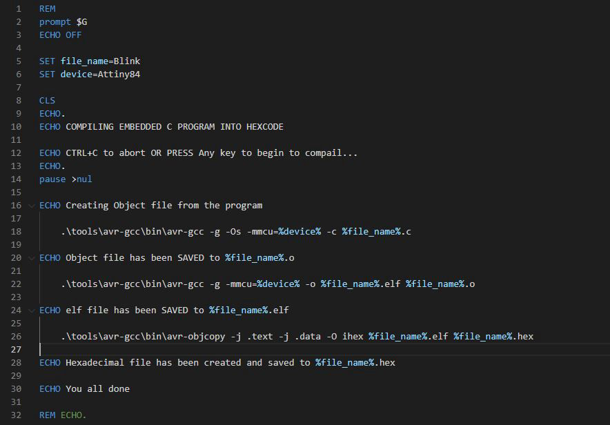
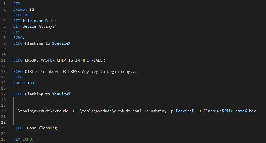
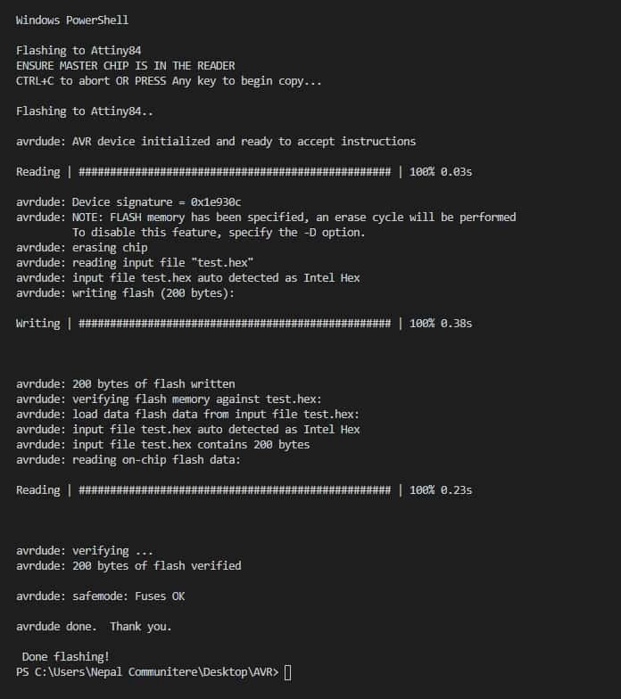
Then for flashing the program
Time to program and flash
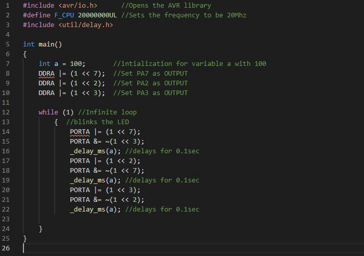
After knowing the process, I used the embedded c programming in visual studio code to blink the LED in the same board.
Save the program and replace the file name in the hex file and then a hex code is generated by using "hex.bat"
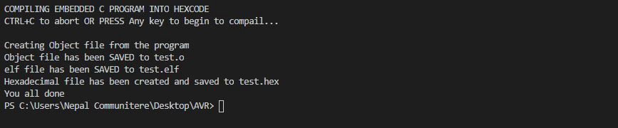
Hex code generated
Then after generating hex file, replace the file name in the flash file as well and the flashing was done using "flash.bat"
Then I tried adding a switch and then programmed as shown as below
#include
#define F_CPU 20000000UL //Sets the frequency to be 20Mhz
#include
int main()
{
int a = 100; //intialization for variable a with 100
DDRA |= (1 << 7); //Set PA7 as OUTPUT
DDRA |= (1 << 2); //Set PA2 as OUTPUT
DDRA |= (1 << 3); //Set PA3 as OUTPUT
DDRB &= ~(1 << 2); //Set PB2 as INPUT
PORTB |= (1<<2); //sets INPUT pin high
//Blinks all LED at once when connected
//Turns on the LED
PORTA |= (1 << 7); //Put high value at PA7
PORTA |= (1 << 3);
PORTA |= (1 << 2);
_delay_ms(a * 10); //delays for 1 sec
//Turns off the LED
PORTA &= ~(1 << 3);
PORTA &= ~(1 << 7);
PORTA &= ~(1 << 2);
while (1) //Infinite loop
{
if (!(PINB & (1<<2))) //checks PB2 is low or not
{ //blinks the LED
PORTA |= (1 << 7);
PORTA &= ~(1 << 3);
_delay_ms(a); //delays for 0.1sec
PORTA |= (1 << 2);
PORTA &= ~(1 << 7);
_delay_ms(a); //delays for 0.1sec
PORTA |= (1 << 3);
PORTA &= ~(1 << 2);
_delay_ms(a); //delays for 0.1sec
}
else
{ //turns off all LEDs
PORTA &= ~(1 << 7);
PORTA &= ~(1 << 3);
PORTA &= ~(1 << 2);
}
}
}
I tried different programs then to switch it on when clicked and switch off when again clicked. That means that each consecutive clicks would be inverting the state of LEDs. You can see the results below.
I came to know that the more high level language it is the longer is the hex code. As we can can Compare hex code generated by Arduino IDE with AVR GCC, the AVR GCC is shorter. Ardino is more easier to user which uses the code in the background.
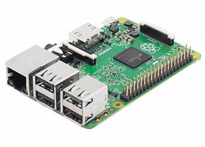
Raspberry Pi: ARM ARCHITECTURE
ARM, previously Advanced RISC Machine, originally Acorn RISC Machine, is a family of reduced instruction set computing (RISC) architectures for computer processors, configured for various environments.Processors that have a RISC architecture typically require fewer transistors than those with a complex instruction set computing (CISC) architecture (such as the x86 processors found in most personal computers), which improves cost, power consumption, and heat dissipation. These characteristics are desirable for light, portable, battery-powered device-including smartphones, laptops and tablet computers, and other embedded systems.] For supercomputers, which consume large amounts of electricity, ARM could also be a power-efficient solution. Most of our mobile phones are based on ARM and now it used on server's and super controllers. Raspberry Pi is Single board computer that based on ARM.
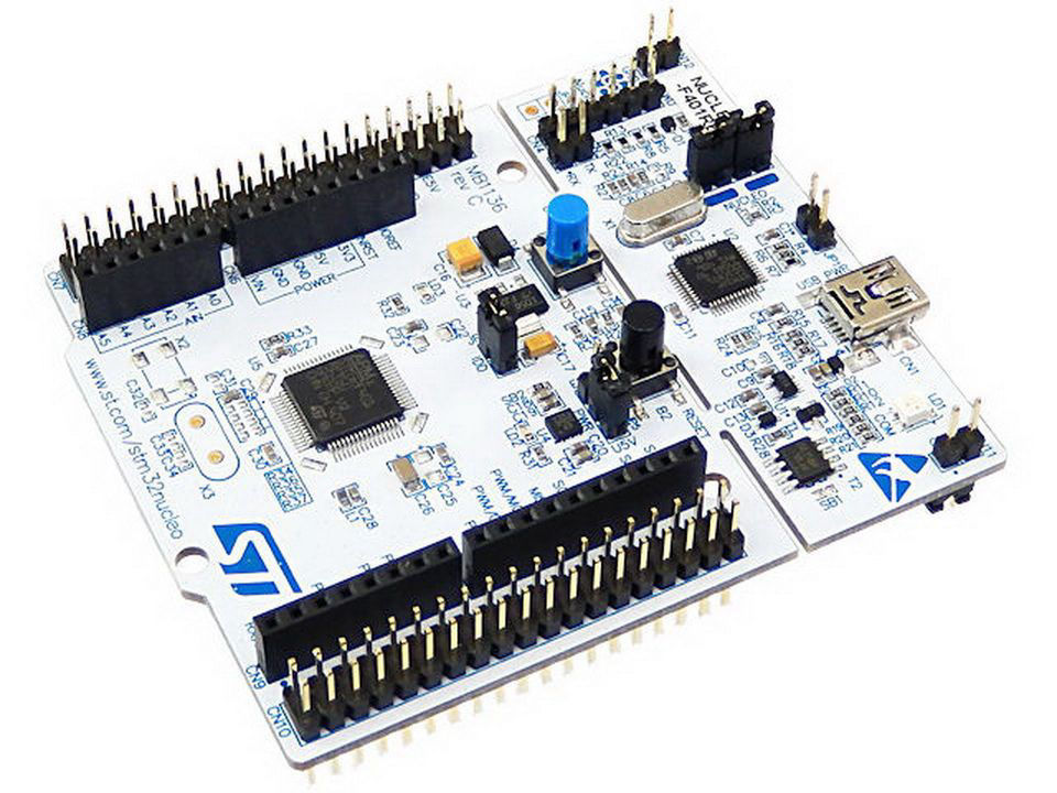
Nucleo STM32F401
STM32 is a family of 32-bit microcontroller integrated circuits by STMicroelectronics. The STM32 chips are grouped into related series that are based around the same 32-bit ARM processor core, such as the Cortex-M7F, Cortex-M4F, Cortex-M3, Cortex-M0+, or Cortex-M0. Internally, each microcontroller consists of the processor core, static RAM memory, flash memory, debugging interface, and various peripherals. In here Fablab Kochi we have the STM32F401 series Nucleo development boards.it's a part of the STM32 Dynamic Efficiency™ device range. These devices offer the best balance of dynamic power consumption (in run mode) and processing performance, while integrating a high number of added-value features in packages as small as 3 x 3 mm. The MCUs deliver the performance of Cortex®-M4 core with floating point unit, running at 84 MHz, while achieving outstandingly low power consumption values in run and stop modes. You can know detail description in my teammate, Saheen Palayi's document.
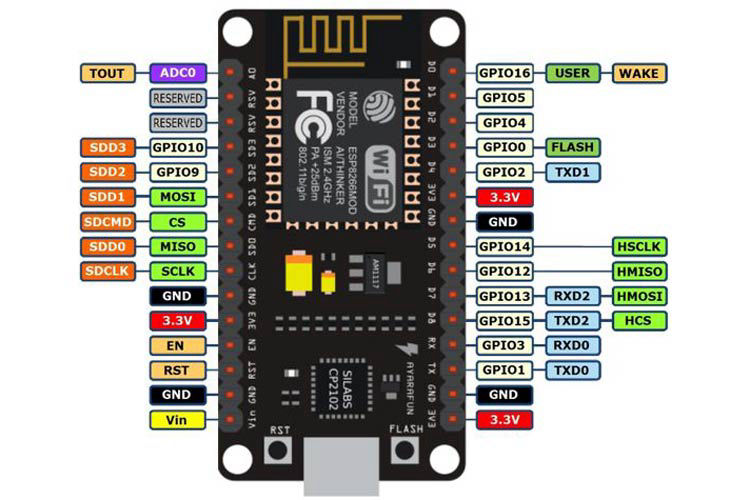
NodeMCU ESP8266
The NodeMCU (Node MicroController Unit) is an open-source software and hardware development environment built around an inexpensive System-on-a-Chip (SoC) called the ESP8266. The ESP8266, designed and manufactured by Espressif Systems, contains the crucial elements of a computer: CPU, RAM, networking (WiFi), and even a modern operating system and SDK. That makes it an excellent choice for the Internet of Things (IoT) projects of all kinds. However, as a chip, the ESP8266 is also hard to access and use. You must solder wires, with the appropriate analog voltage, to its pins for the simplest tasks such as powering it on or sending a keystroke to the “computer” on the chip. You also have to program it in low-level machine instructions that can be interpreted by the chip hardware. This level of integration is not a problem using the ESP8266 as an embedded controller chip in mass-produced electronics. It is a huge burden for hobbyists, hackers, or students who want to experiment with it in their own IoT projects.To know more about NodeMCU please refer this this document form my Teammate Abhinav Ajith.
Lattice ICEstick Evaluation Board 40HX1K
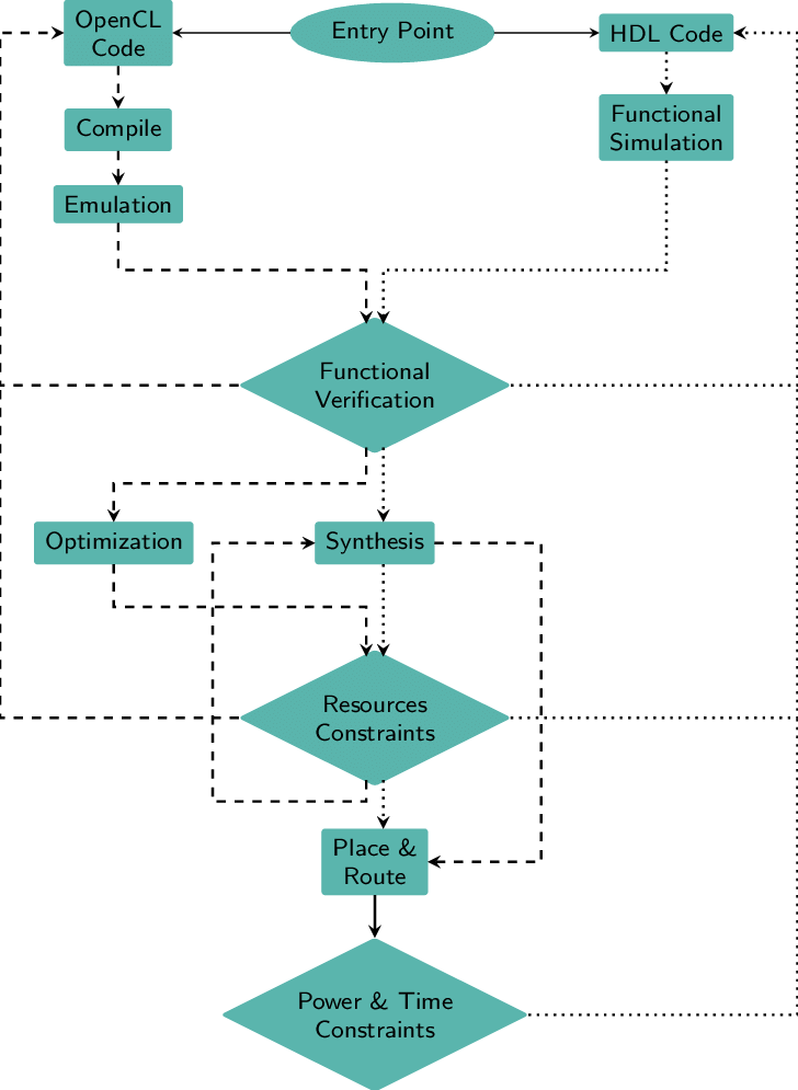
Though we had to explore boards with different architectures, I woked with our goup to know about architectures as mentioned above and came up with this board which was different. This was the board which allows to set it to any architectures. This is called FPGA board meaning Field Programmable Gate Array. Field Programmable Gate Arrays (FPGAs) are semiconductor devices that are based around a matrix of configurable logic blocks (CLBs) connected via programmable interconnects. FPGAs can be reprogrammed to desired application or functionality requirements after manufacturing.
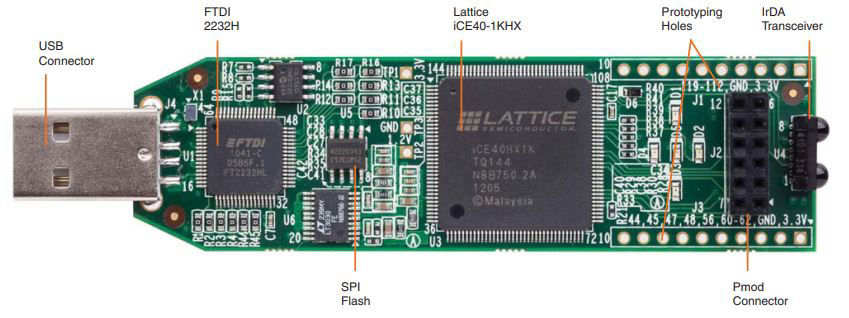
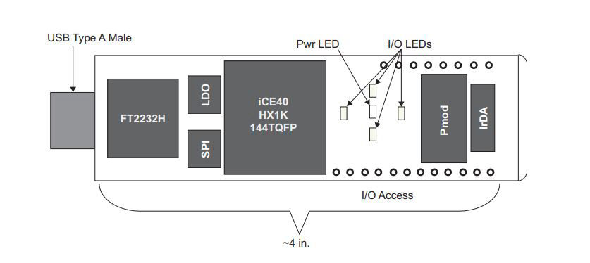
Block diagram
You can download the manual of the Lattice Ice 40HX1K in here.
The beauty of this board is that we can arrange this board in such any way we can. We can test any schematic and architecture in this board. This is a perfect device in which you can use to prototype the PCB and controllers. It contains array or electronic components which is connected according to your input and requirement without hassle of making new board.
You need two software to run it. First to arrange the array of the electronic components according to your requirement. We can use "iCEcube-2" to perform this operation. Then we can use other embedded programming language to flash the board.
Lattice Ice requires the preparation of two text files. The first is a *.v standard Verilog file. The second is a *.pcf pin assignment file that correlates the inputs and outputs declared in the Verilog code to the physical I/O pins on the FPGA.
[UPDATE] My colleague Saheen Palayi has done detail description about Lattice Ice 40HX1K in his documentation. Please click this link to access the documentation for the workflow.
Designed with Mobirise