Assignment
-
Group Assignment
-
Individual assignment:
- Redraw an echo hello-world board,
- Add (at least) a button and LED (with current-limiting resistor)
- Check the design rules, make it, and test it
- Extra credit: simulate its operation
Group assignment
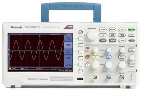
This week we have to test different electronic equipment like multimeter ,DSO, power supply.To know how to used them is equally important as others.I studied DSO and let others fab mate know about DSO.
A digital storage oscilloscope (often abbreviated DSO) is an oscilloscope which stores and analyses the signal digitally rather than using analog techniques. It is now the most common type of oscilloscope in use because of the advanced trigger, storage, display and measurement features which it typically provides.
The input analogue signal is sampled and then converted into a digital record of the amplitude of the signal at each sample time. The sampling frequency should be not less than the Nyquist rate to avoid aliasing. These digital values are then turned back into an analogue signal for display on a cathode ray tube (CRT), or transformed as needed for the various possible types of output—liquid crystal display, chart recorder, plotter or network interface.
What can oscilloscope measures?
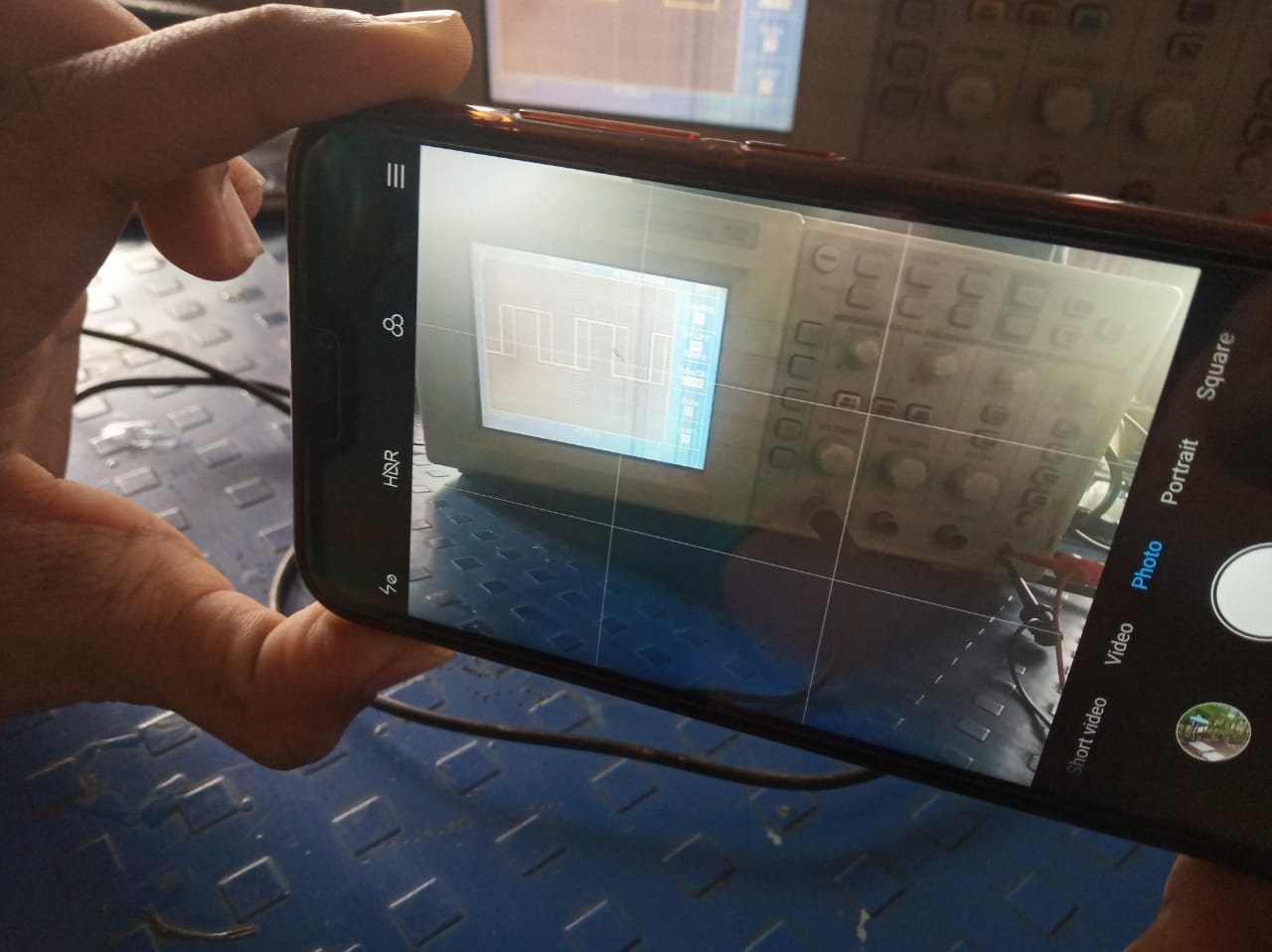
Before we used DSO first make sure is it working properly or not?For that take the test of DSO.Most of the DSO is having in built frequency conductor one for the signal and one for the ground.Connect Red and black probe of DSO into signal and ground respetively.Then observed the screen of DSO if the square pulse start appearing then DSO is working fine otherwise not.
Basic electronics:
There are many ways to classify different types of electronic components but the most common way is to classify them in to mainly two types:
1)Active Electronic Components
2)Passive Electronic Components
1)Active Electronic Components
Active components are defined as the devices that depend on energy source and can introduce power into a circuit.
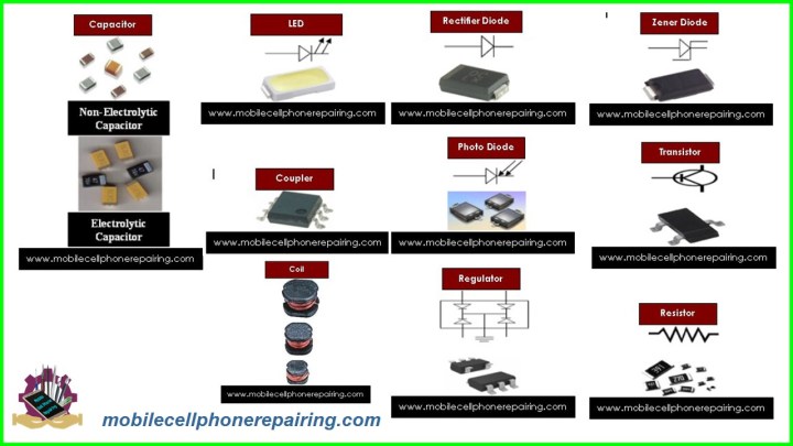
Diodes: A diode is a non-linear semiconductor device, that allows the flow of current in one direction. A Diode is a two – terminal device and the two terminals are Anode and Cathode respectively. The following is the symbol of a Diode.
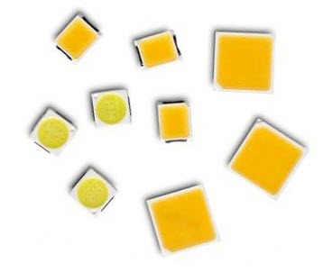
LED: An LED or a Light Emitting Diode is semiconductor device that emits light due to Electroluminescence effect. An LED is basically a PN Junction Diode, which emits light when forward biased.
2)Passive Electronic Components
Passive Components cannot control the flow of current through them i.e. they cannot introduce energy in to the circuit but can increase or decrease voltage and current.
These components don’t depend on the energy source for their operation.Two terminal components like Resistors, Capacitors, Inductors and transformers are examples of Passive Components.
Resistors:
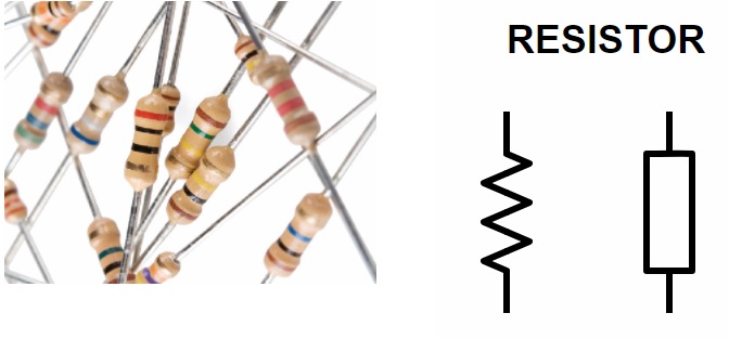
The basic of all electronic components are the Resistors. It is a passive electronic components that introduces electrical resistance in to the circuit. Using resistors, we can reduce the current, divide voltages, setup biasing of transistors (or other active elements), etc.
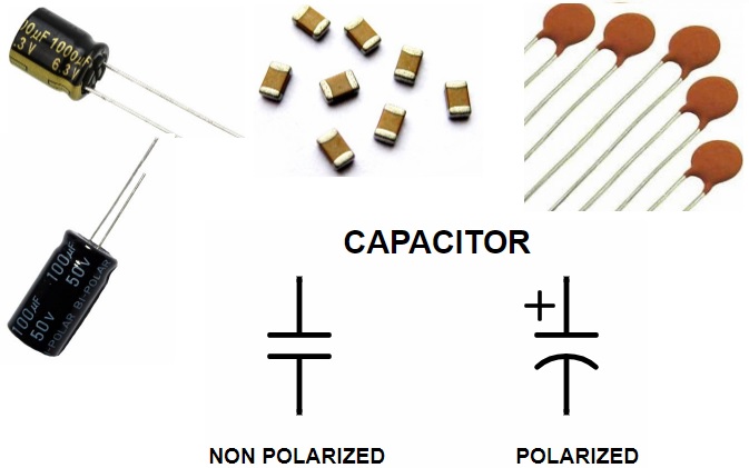
Capacitors:
The second important passive components is a capacitor, a device that stores energy in the form of electric field. Most capacitors consists of two conducting plates that are separated by a dielectric material.
Go get stuff:
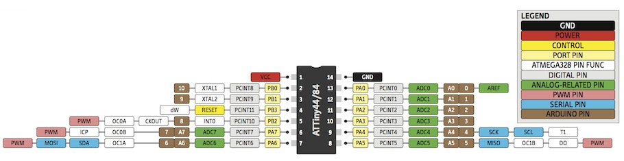
1.What & Why Attiny 44:
ATtiny (also known as TinyAVR) are a subfamily of the popular 8-bit AVR microcontrollers, which typically has fewer features, fewer I/O pins, and less memory than other AVR series chips Refer from Wiki
Features
- ● High performance, low power AVR® 8-bit microcontroller
- ● Advanced RISC architecture
- ● 120 powerful instructions – most single clock cycle execution
- ● 32 x 8 general purpose working registers
- ● Fully static operation
- ● Non-volatile program and data memories
- ● 2/4/8K byte of in-system programmable program memory flash (Atmel®
ATtiny24/44/84)
- ● Endurance: 10,000 write/erase cycles
- ● 128/256/512 bytes in-system programmable EEPROM (Atmel ATtiny24/44/84)
- ● Endurance: 100,000 write/erase cycles
- ● 128/256/512 bytes internal SRAM (Atmel ATtiny24/44/84)
- ● Programming lock for self-programming flash program and EEPROM data
security
- ● Peripheral features
- ● Two Timer/Counters, 8- and 16-bit counters with two PWM channels on both
- ● 10-bit ADC
- ● Eight single-ended channels
- ● 12 differential ADC channel pairs with programmable gain (1x, 20x)
- ● Temperature measurement
- ● Programmable watchdog timer with separate on-chip oscillator
- ● On-chip analog comparator
- ● Special microcontroller features
- ● debugWIRE on-chip debug system
- ● In-system programmable via SPI port
- ● External and internal interrupt sources
- ● Pin change interrupt on 12 pins
- ● Low power idle, ADC noise reduction, standby and power-down modes
- ● Enhanced power-on reset circuit
- ● Programmable brown-out detection circuit
- ● Internal calibrated oscillator
- ● On-chip temperature sensor
2.Componants Sorting:
3.Why eagle ? PCB Design Software
Beginning January 2020, your EAGLE account entitles you to Fusion 360! Student, startup, hobbyist, or professional - get started using the first truly end to end, whole-product design & manufacturing Platform. Electronics Design, eCooling / Thermal Analysis, 3D Modeling, Industrial Design, CNC Machining, 3D Printing, Sheet Metal - one platform, one massive step up! Download eagle
.
Making of PCB board
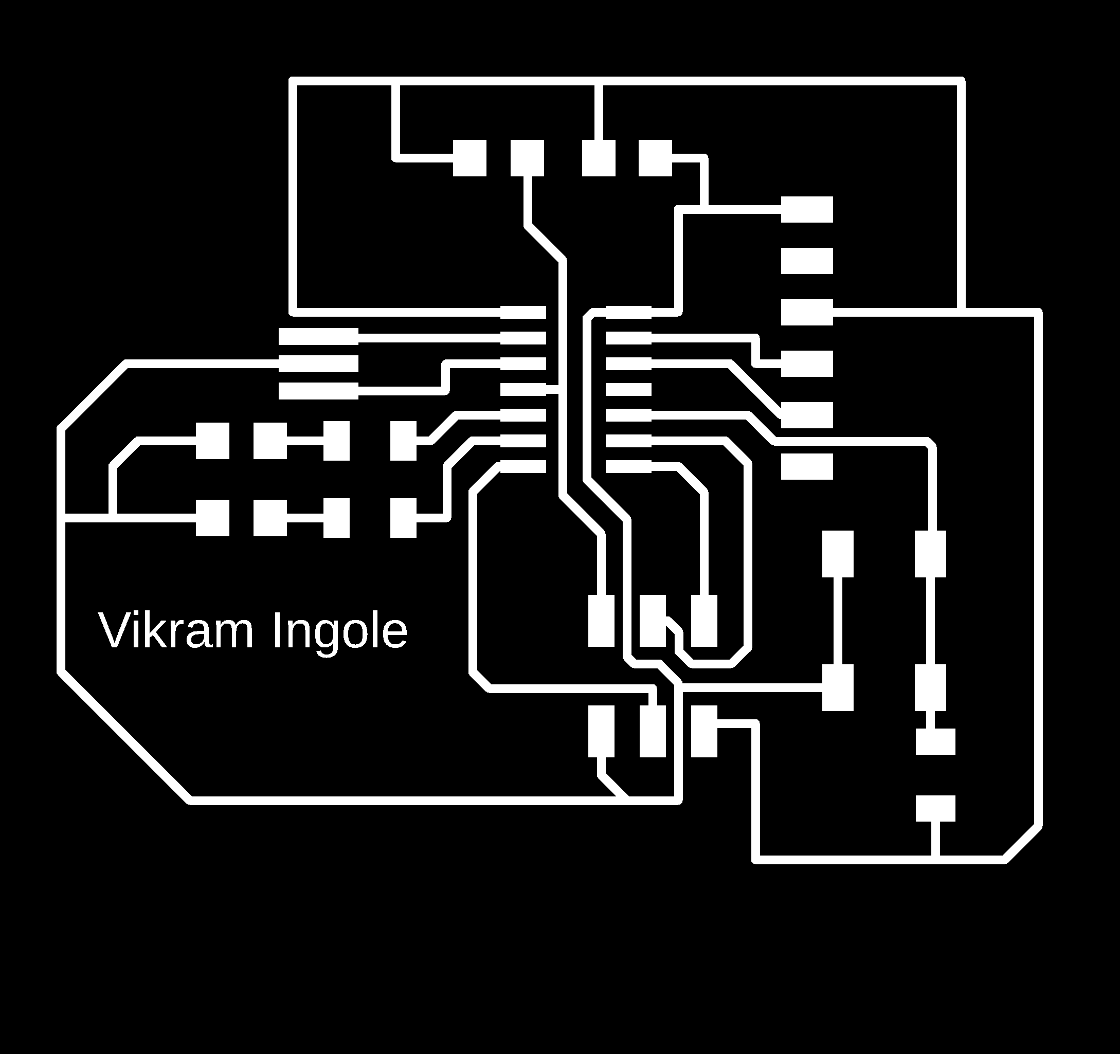
After understanding the importance of above things and their need in whole process then we need to move PCB design part.Here i tried to elaborate the step by step procedure to design my PCB schematic using EAGLE.Gueys what i understood that you need to design your schematic in schematic editor first. Once we finished schematic part then later we switch from schematic to board editor.
Step 1.Create a Schematic file
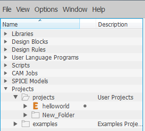
Open EAGLE & right click on project menu & Create first a new project called Helloworld
Step 2.Place symbol
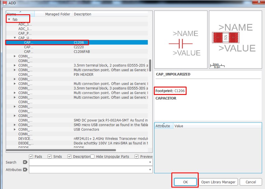
Once you open the schematic window next step is to Add part (componant) into schematic editor from fab library which i add earlier from git just one after the other using add part menu.Use bus and net command , connect up the pins of the various elements on the drawing
Step 3.Name the symbol
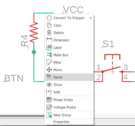
After placeing all required componant into schematic editor start lebaling it with appropriate name which you helped to connect the two componant.
Step 4.Full Schematic
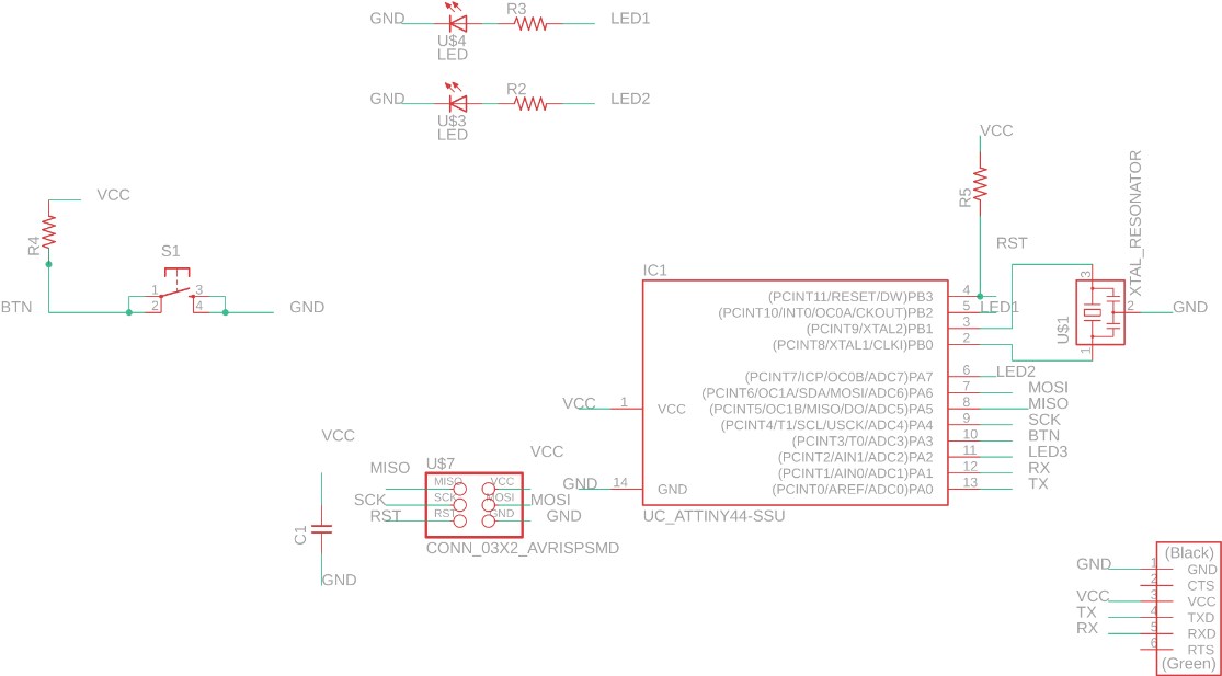
This is a full schematic view where i placed all required componants and interfaced them with Attiny 44 accordingly.Also i placed two leds and one push button.
Just Note
Step 5.Checking Connectivity Errors with an ERC
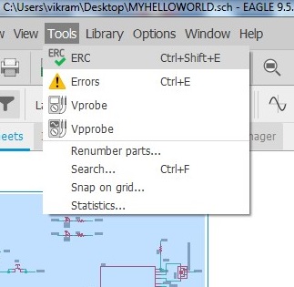
There’s one last step before you can check off on your schematic design and move onto your PCB layout – checking for connectivity with an Electrical Rule Check, or ERC. Let’s do it.
Step 6.Fixing your ERC errors
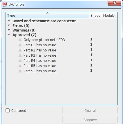
As you can see there’s a whole lot of warnings and one error to review in our schematic. Before moving forward and fixing these, let’s review how this ERC Errors Dialog works.
Step 7.Turning Schematic Into Board Layout
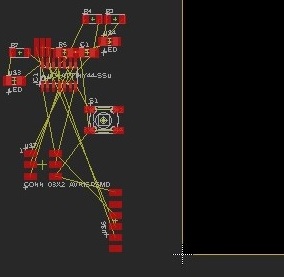
At the top of your interface, select the SCH/BRD sch-brd-icon icon. This will begin the process of generating a PCB layout based on the components and wiring in your schematic.That’s it! You should now have a second Autodesk EAGLE window open that looks similar to ours below.
Step 8.Placeing componant into PCB layout area
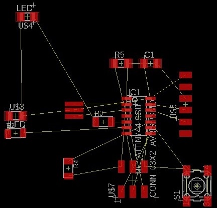
Placeing the componant into the PCB layout area first using move command.After dragging arrange the componants as per your wish.
Step 9.Checking DRC Error
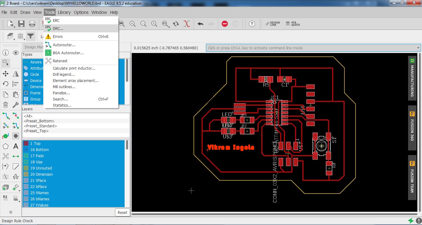
Route the componant using net wires menu and interfaced properly.When i was doing ths stuff next step is PCB manufacturing .But there are some physical constraints that you need to pay attentions.a Design Rule Check allows you to establish a set of boundaries for trace widths, component spacing, via diameters, etc.
Step 10.Layers settings
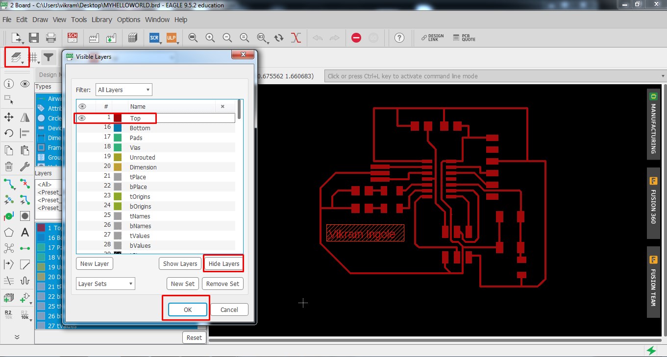
Go to layer setting and hide unwanted layers and prepared to export the PCB layout image
Step 11.Export the PCB layout
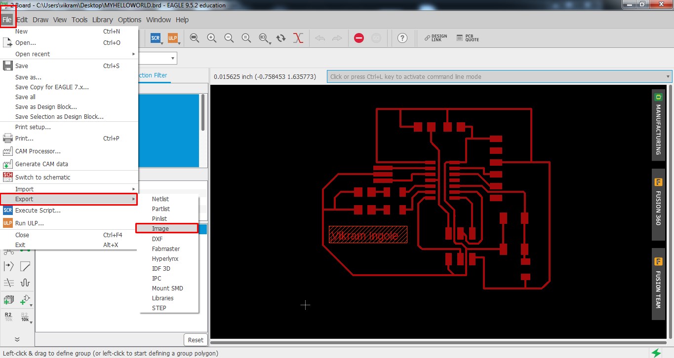
Go to file - export - image.
Step 12.Set the image resolution
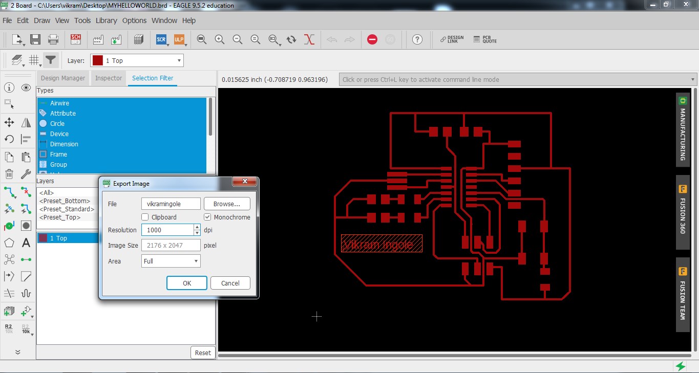
Give file name , select monochrome and 1000 dpi resolutions
PCB Milling
Now this section will give you idea about PCB milling.In our lab, We have SRM -20 PCB milling machine.I have already milled my FAB ISP in electronics production week where you found whole procedure about how to used SRM-20 Electronic production week.To begin the PCB milling work first i need to generate rml file using FAB mod and import this rml file into VPanel third part software.Once you do all required setting start milling my PCB on SRM-20.More documentation found on milling can be found on my Electronics production week, specifically here . The settings I used to mill this board were as follows:
Step 1.Open Fab module -> Select the PNG image -> Select mill traces (1/64) -> Calculate mill raster 2d -> Save the generated .rml file
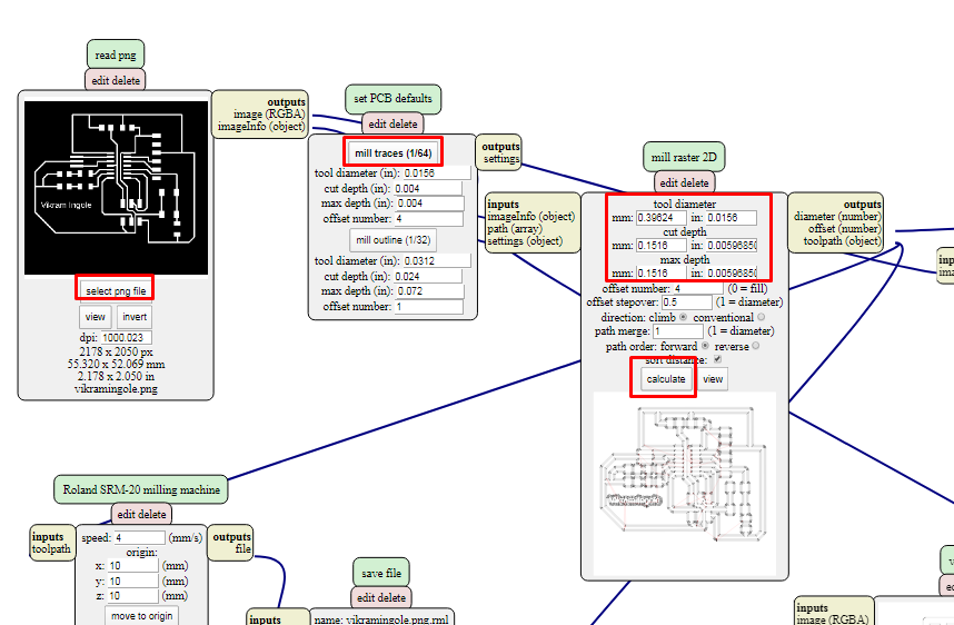
Step2.Turn on SRM-20 -> Open Vpanel S/W -> Do proper setting -> Add the .rml file -> Start milling PCB
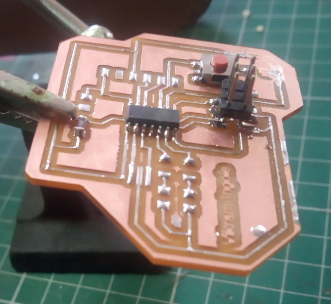
Soldering
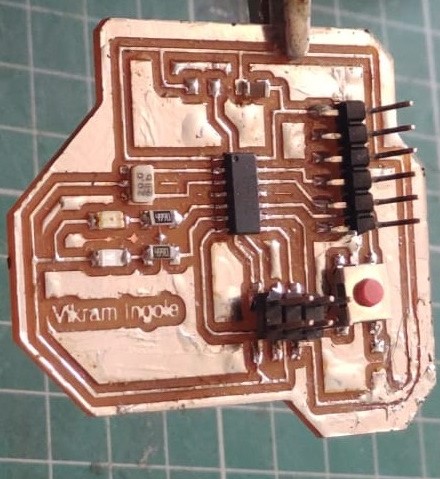
Once i done with PCB milling part now next step is soldered the board.In electronic production week we studied and experienced the some basic rules of how to used the soldering desk properly.So keeping this mind i start soldering the my hello echo board.Also little attension is given to the part which was not properly milled which i have already mentioned in my PCB milling section as well.Lets begin soldering......
Programming
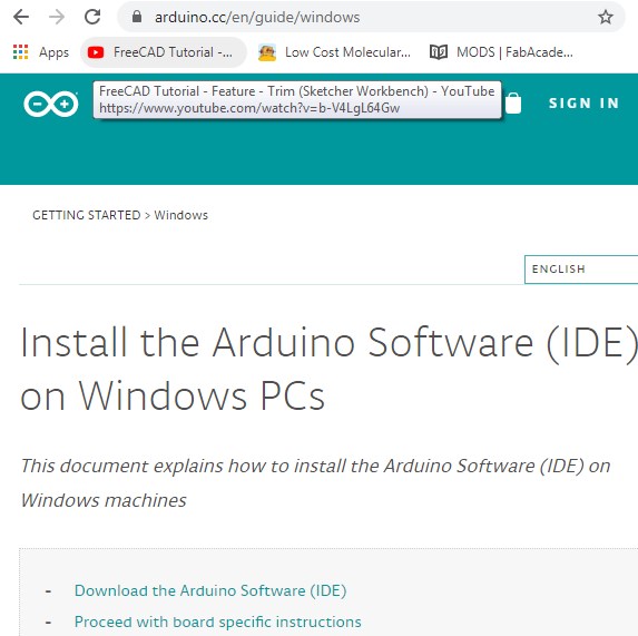
The most intersting and fun loveing part is programming.To finish this part of programming basically i need two things first to programmed my Hello echo board i brought my FAB ISP board which i designed in previous week to programme by hello echo board.Then second thing was IDE where i am going to edit my programe.So i install the Arduino IDE.
1.Collect FAB isp 2.Install IDE
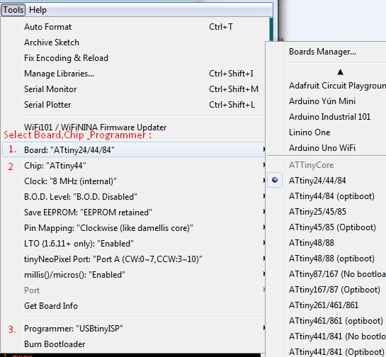
Boards Manager Installation
This core can be installed using the boards manager. The boards manager URL is:
http://drazzy.com/package_drazzy.com_index.json
1.File -> Preferences, enter the above URL in "Additional Boards Manager URLs"
2.Tools -> Boards -> Boards Manager... *If using 1.6.6, close boards manager and re-open it (see below)
3.Select "ATTinyCore by Spence Konde" and click "Install".
- //
-
//
-
// hello.ftdi.44.echo.c
- const int led1=8;
- const int led2=7;
- const int button=3;
- void setup()
- {
- pinMode(led1,OUTPUT);// initialize digital pin 8 as an outputpinMode(led2,OUTPUT);// initialize digital pin 7 as an output.pinMode(button,INPUT);// initialize digital pin 3 as an input.pinMode(button,INPUT);// initialize digital pin 3 as an input.}void loop() {// put your main code here, to run repeatedly:if (digitalRead(button)==HIGH)// read the input pin:{digitalWrite(led2,HIGH);// turn the LED on (HIGH is the voltage level)}else if (digitalRead(button)==LOW)// read the input pin:{digitalWrite(led2,LOW);// turn the LED off (LOW is the voltage level).}
Errors overcome
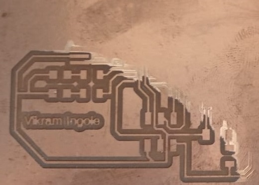
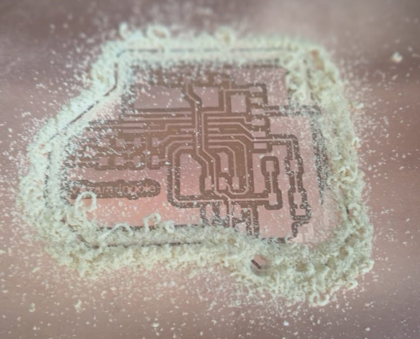
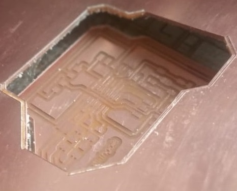
PCB milled with left part When i start milling my board it was not properly milled by SRM-20.There are several reason to cause this happend.First possibilities might be related to sacrificial surface so we checked it but it won't work and its perfactly fine.Then We found that Copper plate surface is somewhat uneven and actually there was very littile curve in the plate.It was not flat enough.So to resolve this issue we change/increase the cut depth .Due to increase in cut depth,the left part of PCB was milled properly.
Proper milled PCB