Project Development
This part of the course was longer for me than a couple of weeks. I managed to find access to a lab - FabLab UAE and am very thankful to Hashim for letting me use the resources of the Lab, and Steven for setting this up for me.
Page Summary
- Project Management
- Tracking progress
- Development
- Important and interesting links
1. Project Management
Murphy’s Law - everything that can go wrong will go wrong. This has happened many a times for me in respect to FabAcademy.
Triage - I have some trouble with this. As I get easily distracted and go into the depth of things without zooming out in time to finish the assignments.
Documentation during development - Fighting procrastination to get better with this.
Demand- vs supply-side time management - Generally I used this for the last 2-3 weeks before the final project submission deadline.
Spiral development, DevOps - This is my favourite. I have started using this in my design practice and various other aspects of life.
Serial vs parallel tasks - I do both depending on the task, the time and the surrounding contexts.
System integration - getting better and better at this with time, documenting this is very difficult because of non compartmentalisation.
Finish quality - I believe in using materials in an honest way to hero their intrinsic properties and not hide them under aesthetic finishes. This makes the underlying parts neat and organised automatically.
2. Tracking progress
What tasks have been completed, and what tasks remain?
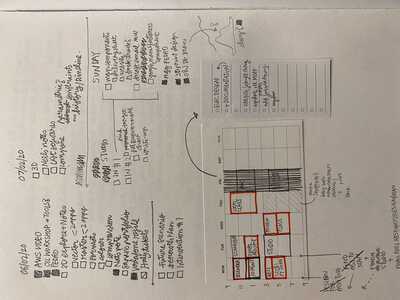
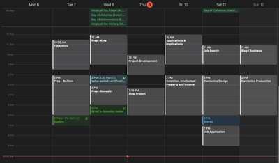
I kept a record of this by making a to-do list every week in my notebook and then assigning time for each task in my calendar. Here are some pictures of my to-dos:
What’s working? What’s not?
The OLED screen I borrowed from the lab, stopped working after I tried it with an Arduino Uno. I’m not sure what was wrong, but I checked every connection with a multimeter. I tried an I2C scanner detector but it still did not detect the device. I also tried it with a different programming board, and a I2C LCD screen with the same board. But after testing each connecting part, something in the OLED did not work. So finally, I got a new one.
The laser cutter I used at the Lab - a Universal Laser system, had a different kerf in the x-axis and the y-axis. I tried many different combinations of settings and materials. But still could not figure out how to fix this. Eventually I offset my tongue and groove joints different in X- and Y- directions.
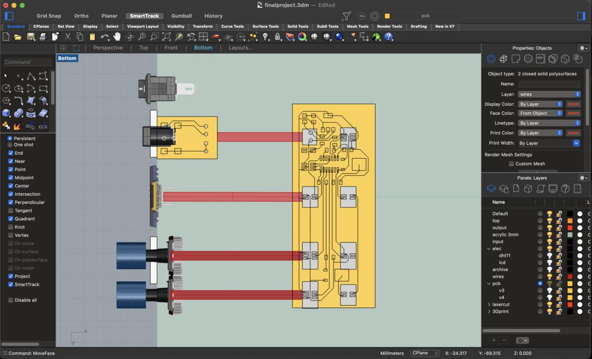
I designed and made my PCB using an ATtiny44 microcontroller. Early on I figured that all the different libraries I would need to work the DHT11 and the OLED would not fit in the 4k storage space. So I desoldered the 44 and used an ATtiny84, so that nothing would change but the microcontroller. Eventually I discovered the tiny libraries for OLED and DHT - optimal versions of the full libraries and turned out the code used only 4136 bytes of storage space.
I made the first layout of the PCB trying to make it as compact as possible by keeping parts close together and traces more optimised on space.
Eventually, I changed the layout of the header pins that connect to all different input/ out puts and matched them to their physical location on the machine. This resulted in a much bigger PCB but a very neat layout of all the wiring. I planned it such that the wiring would neatly stretch on the side of the machine, but Neil suggested using a cable manager instead.
I also wanted to add a mobile application to control the machine instead of the physical regulators and switches as the last spiral development cycle including a wifi module.
What have you learned?
Through this project I learnt the most in electronics design and programming. The process of ‘How to design a PCB from scratch for what you want the thing to do’ as described in the weekly documentation was the most empowering.
3. Development
Process
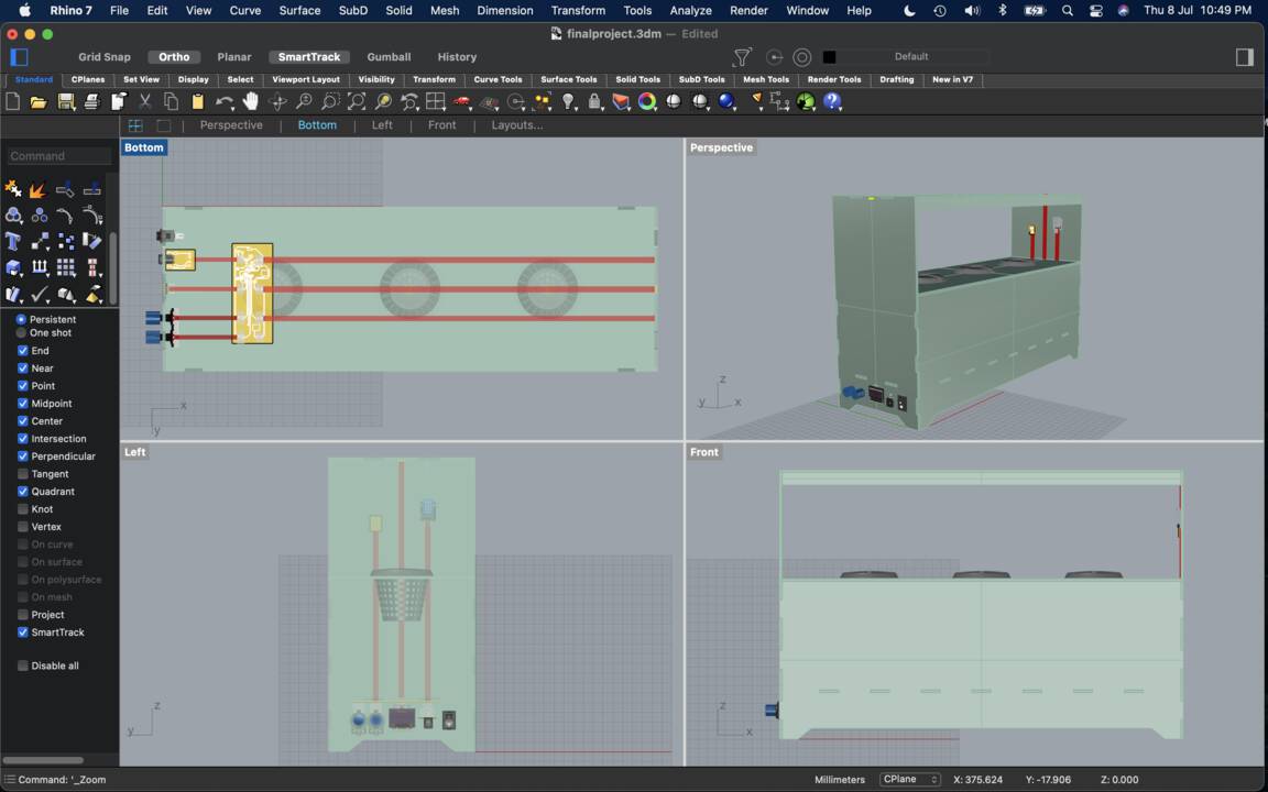
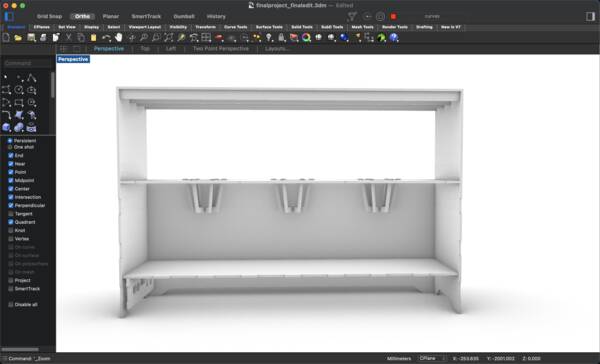
* First I started by making a CAD model in Rhino. I explored multiple forms.
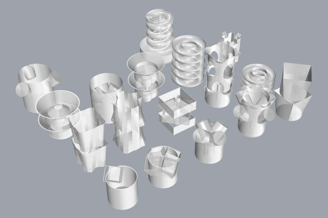 Since I need to make as many parts as possible in the lab instead of buying parts, I modify the design to make it less curved and simpler to cut and assemble.
Designing the electronics:
Inputs to include:
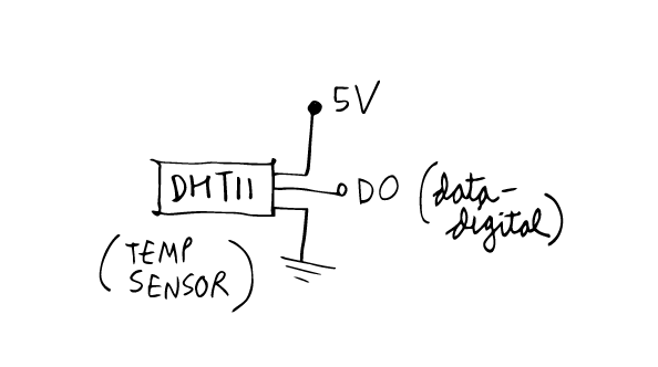
- DHT11 - temperature and humidity sensor
- Phototransistor - to measure ambient light intensity
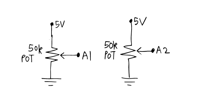
- Potentiometer / variable resistance - to control flow of water through pump
- Potentiometer / variable resistance - to control grow light intensity
- Toggle switch for power on/off
Outputs are:
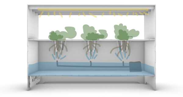
- 12V DC pump to pump water through a sprinkler system
- 12V DC growth light strip with 3:1 RB 5050SMD LEDs
- SSD1306 OLED screen with I2C
With the help my instructor Steven, I developed a basic scheme for the electronics.
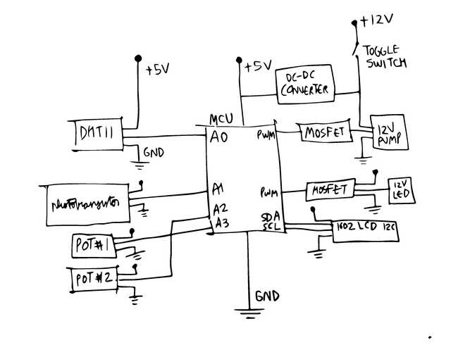
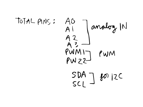
Also counting the pins required for each sensor and actuator:
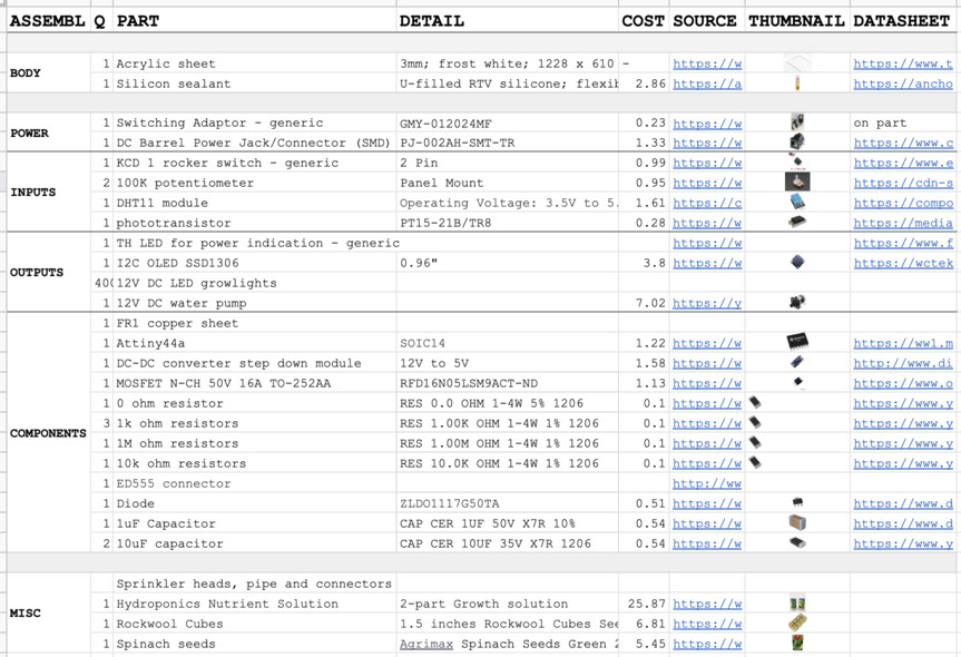
Since I am not in the lab, I need to order some components myself. I start making a Bill of Materials for the project electronics:
Next, I started making a schematic according to the sketch, connecting each component to V, GND and respective pins.
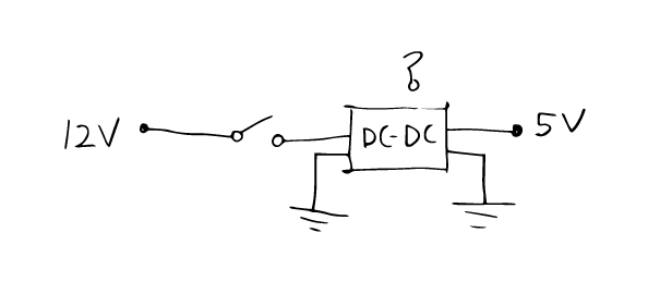
12V DC-DC converter to 5V
The DC-DC converter will have connections based on the datasheet…
I’m connecting a toggle switch to the converter, which will be the power on/off switch for the user
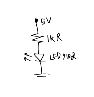
I’m also adding a red SMD LED as a power indicator.
Phototransistor has two options of circuits, according to this guide.
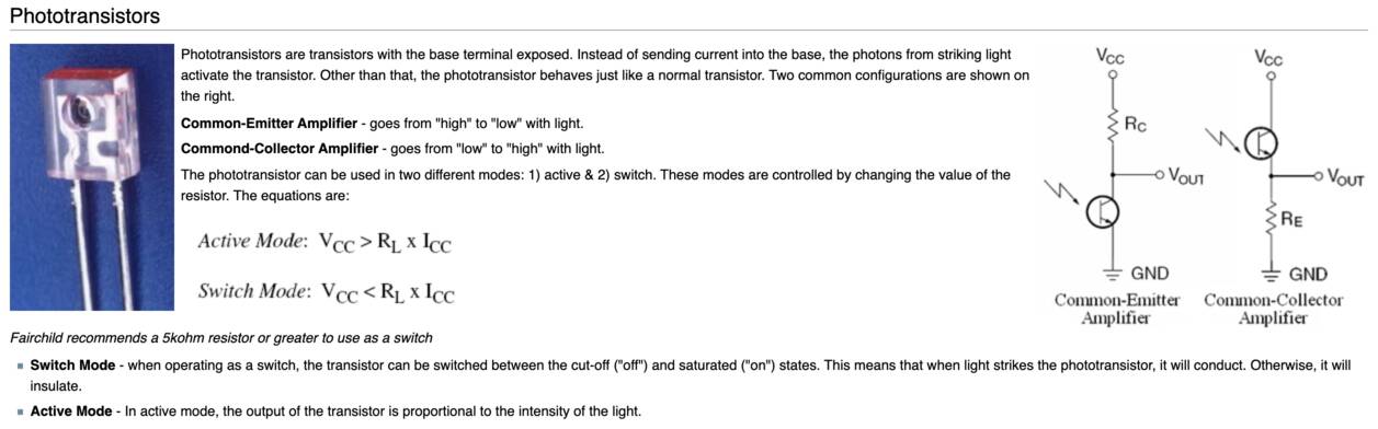
I use the Phototransistor in active mode - meaning the output of the transistor is proportional to the intensity of the light.
![]()
The potentiometers have 3 pins - one for power, one GND and third data that connects to the MCU.
The temperature and humidity sensor DHT11 has 3 pins - 5V power, GND and data which connects to a digital pin of the MCU.
Ref: Introduction to DHT11
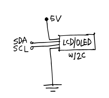
I use an OLED SSD1306 with I2C to make serial communication easier and use less pins on the MCU, only SDA and SCL.
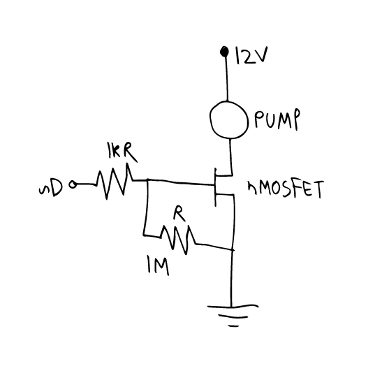
A 12V DC water pump is connected to the MCU with a n-channel MOSFET so I can control the flow of water using Pulse Width Modulation.
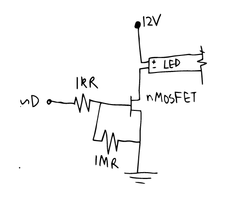
Similarly the 12V DC LED growlight strip is connected to the MCU with a n-channel MOSFET so I can control the light intensity. These come in different ratios of red-blue lights. I plan to use one with 3:1 meant for leafy plants.
Next, I use KiCAD to put all these schematics together and begin to design my PCB.
While making the schematic I realise not all sensors and actuators need to be on the PCB itself, some like the pump and the LED and the DHT11 need to be at a different physical location on the designed box, so I need to add header pins and connect them using wires later.
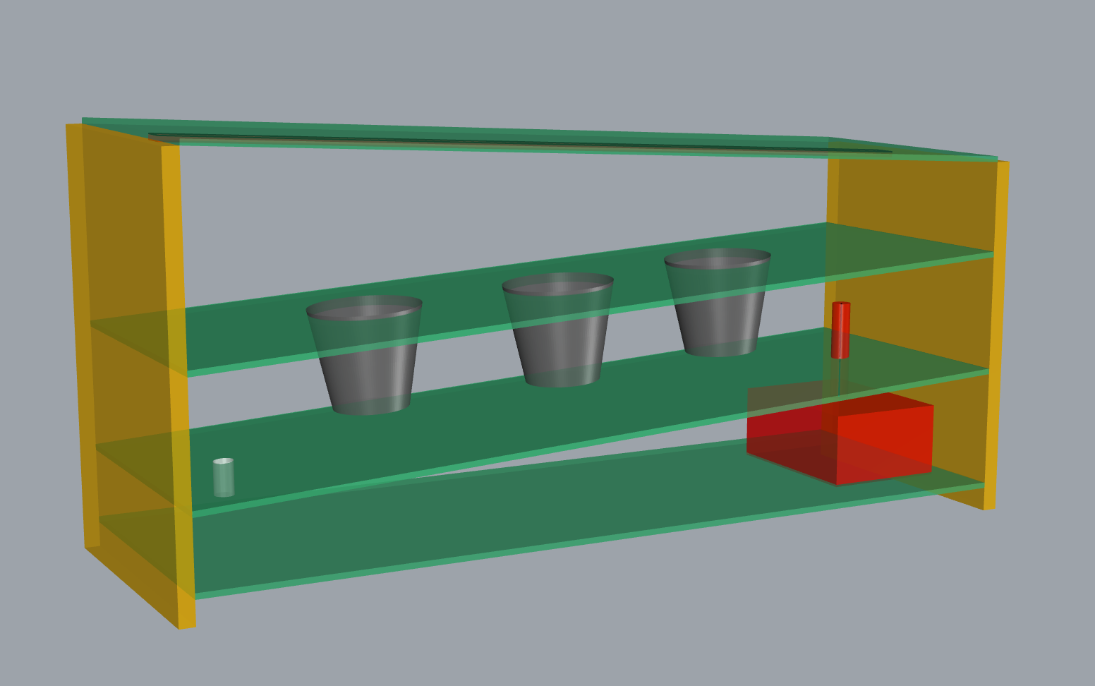
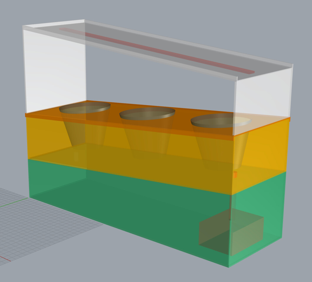
To clarify this, I begin modifying my 3D CAD model on Rhino.
And then redo the schematic.
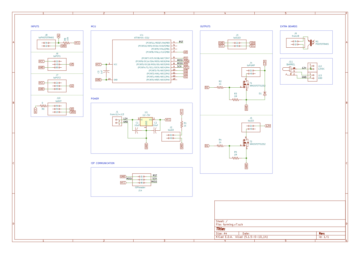
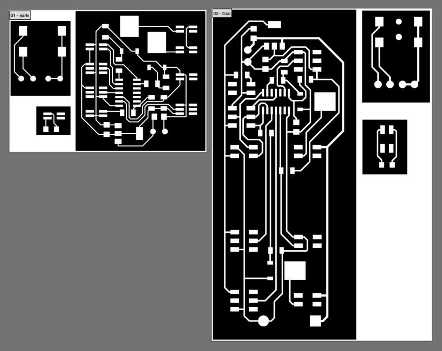
Next, I generate the Netlist and load it in the pcbnew of KiCAD. I arrange all header pins in a linear fashion so that they do not get jumbled and don’t cross each other like in the model.
After about 7 revisions, changing minor details, I made
Here are the final design files for the board:
Schematic v7
Traces png
Outline png, containing the holes too.
Things to do next:
Milling prcoess Soldering Components Testing board Connecting all inputs and outputs
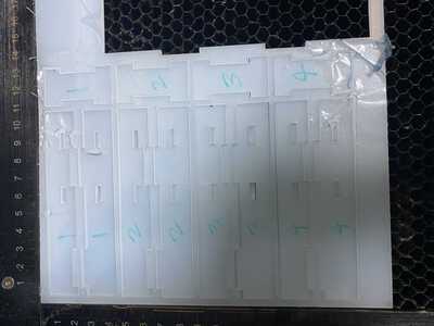
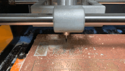
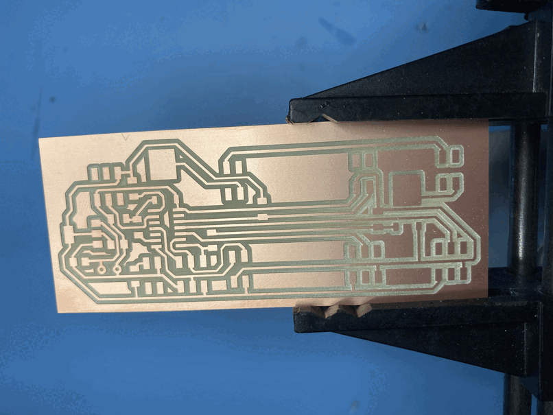
Milling the PCB
I followed all the settings and the workflow as described in the Electronics Prdocution week documentation and milled the board:
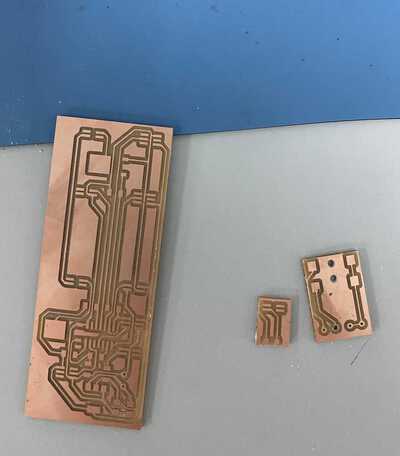
These are the 3 final boards:
Soldering components
After making a ‘shopping list’ I gathered all components. Most of them were available from the Lab (FabLAb UAE).
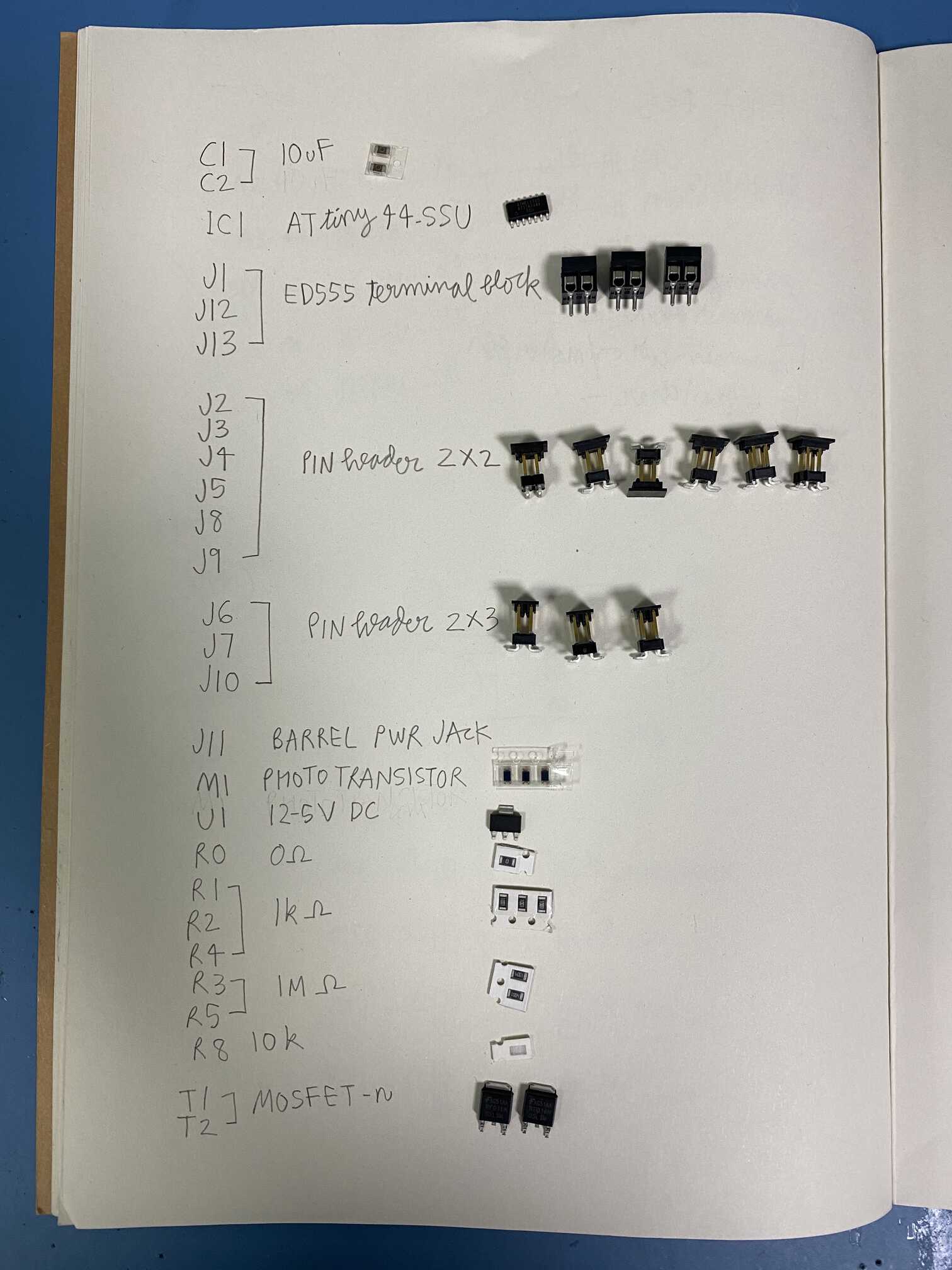
As good standard practice, I soldered all components from left to right and top to bottom. Starting with the microcontroller, then smaller components like resistors, capacitors, then the larger mosfets and DC-DC voltage regulator and all the header pins in the end.
Testing board
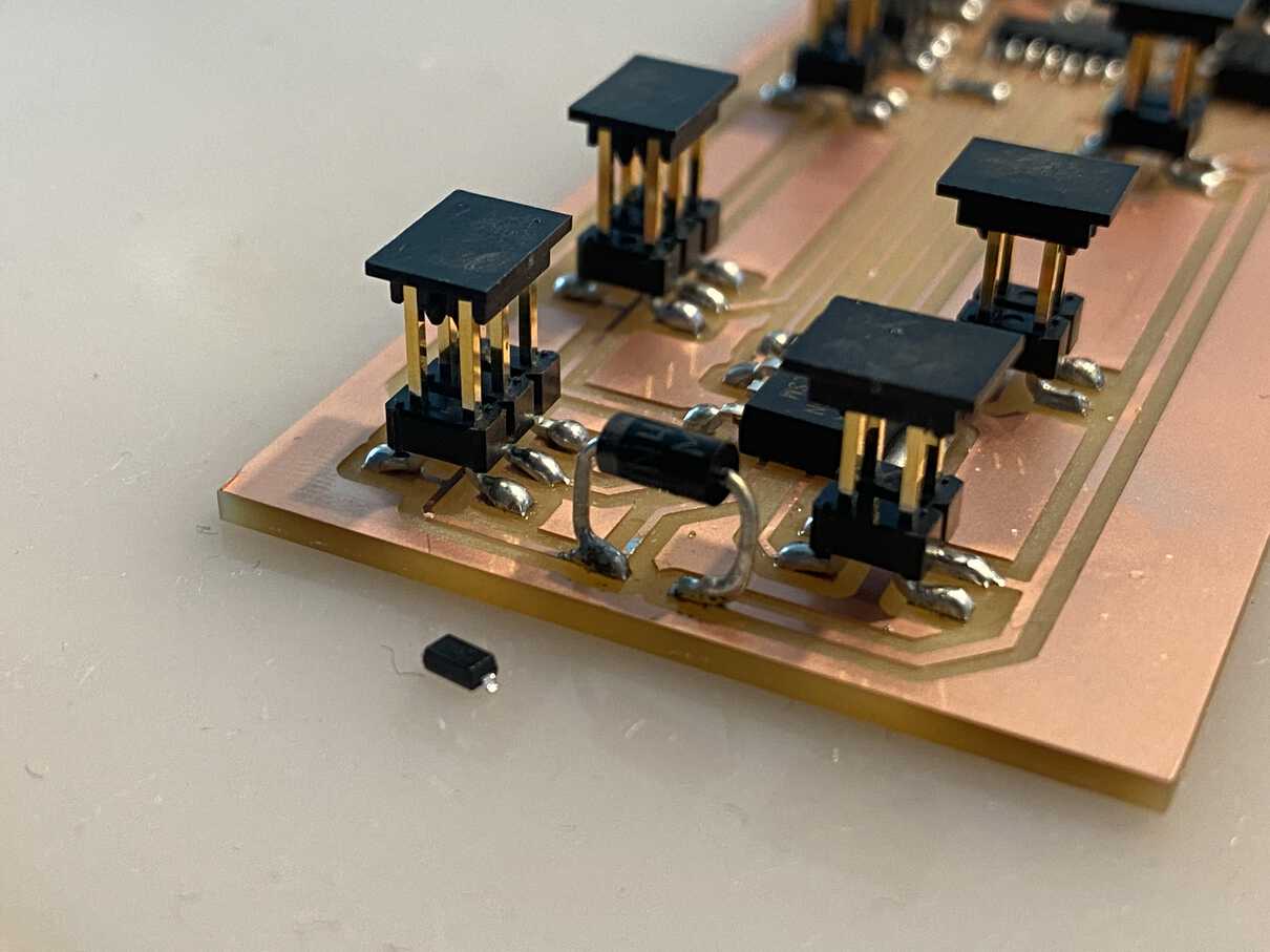
I was missing a diode. Since this wasn’t in the lab, I used a TH component, cut legs and soldered it directly onto the copper tracks. It was a little delicate, but it worked. I had to make sure it was connected in reverse to save the DC outputs from burning.
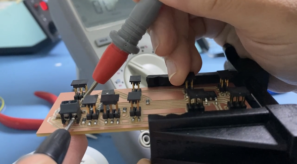
I also cleaned up the board for copper shards and tested all connections using a multimeter. Beeping all VCC, GND connections to themselves and measuring resistance across al resistors.
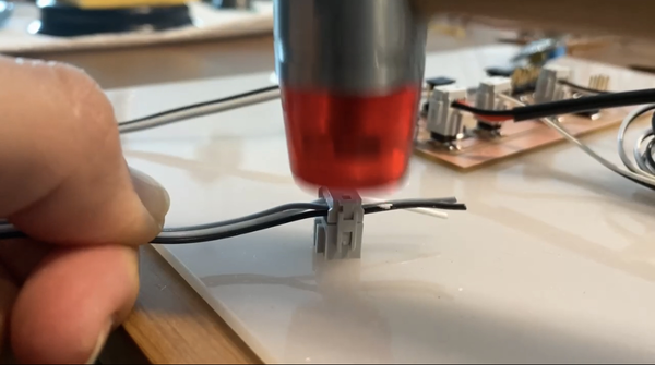
Wires and wiring
I used ribbon cable and cut them to custom lengths according to the 3D model. And hammered on header pins with 2x rows instead of 1, to make the connections sturdier.
Programming:
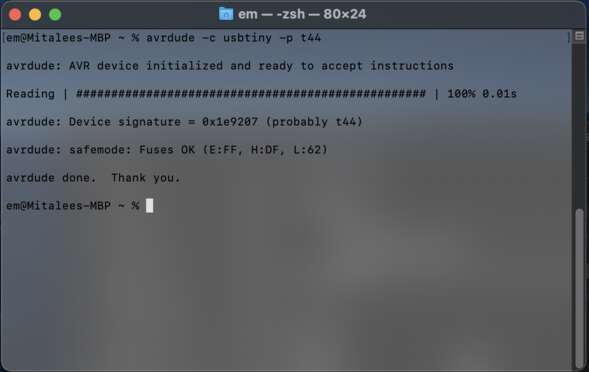
I will use the FabISP I made in Electronics Production week as a programmer to program my farming board with all the inputs and outputs.
AVRDUDE is a utility to download/upload/manipulate the ROM and EEPROM contents of AVR microcontrollers using the in-system programming technique (ISP).
- Connect the new board with a ribbon cable to the FabISP programmer through a compatible USB adaptor.
Check the orientation of the cables is in correct order. VCC of the FabISP matches the VCC of the target board(mine with ATtiny44) Check System Report > Hardware > USB, should detect the USBtinyISP.
Next in a terminal window,
avrdude -c usbtiny -p t44
It should show that the device is initialized and show a signature.
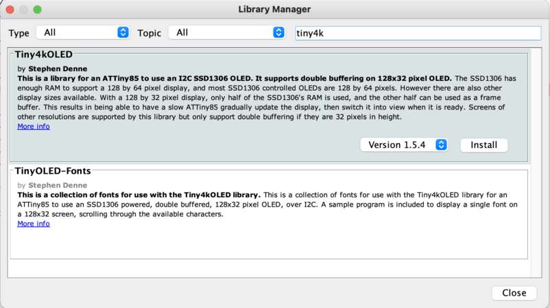
Next, I will start adding the i/o one by one starting with the OLED so I can use it as a display for troubleshooting along the way. Since I’m using a Attiny44 with 4k memory, I will use the minimal versions of OLED and DHT libraries to make enough space for the rest of the components.
- Install OLED library from https://github.com/datacute/Tiny4kOLED which is a Library for an ATTiny85 to use an SSD1306 powered, double buffered, 128x32 pixel OLED, over I2C.
Open Arduino IDE, in Tools > Board Manager, add the https://github.com/technoblogy/tiny-i2c in additional boards URLs.
Sketch > Include Library > Manage Librarries, select Tiny4kOLED and install.
3D printing
Knobs for potentiometers: [3D model]
Gcode file has these settings:
TARGET_MACHINE.NAME:Ultimaker 3 Extended
Material= PLA
EXTRUDER_TRAIN.0.INITIAL_TEMPERATURE:205
EXTRUDER_TRAIN.0.NOZZLE.DIAMETER:0.4
BUILD_PLATE.INITIAL_TEMPERATURE:60
Print Quality = normal
Adhesion type = none
Supportenable = True
nbottom_layers = 12
ngradual_infill_steps = 5
ninfill_pattern = concentric
ll_sparse_density = 50
nsupport_angle = 30
ntop_bottom_thickness = 1.2
nwall_thickness = 5
Printing took approx. 27 minutes plus heating and cooling time…
2D and 3D design
I started by sketching out ideas on paper.
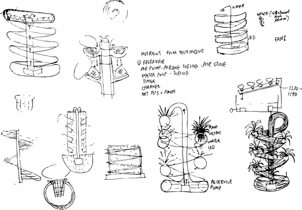
Then after figuring out basic elec requirements, I used Rhino to design the model with all electronics in 3D.
I also made a quick render in Rhino and made a 2D illustration to sketch out ideas.
Here is the 3D model:
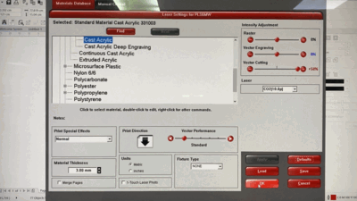
Lasercutting
I followed the same workflow as computer controlled cutting week documentation to cut the acrylic for the body.
Last, part was assembly and filling in all components together.
program code, assembly & testing process.
4. Important and interesting links
Project Development class notes + video
KICAD symbol and footprint guide