7. Electronics design
group project:
      use the test equipment in your lab to observe the operation
         of a microcontroller circuit board
   individual project:
      redraw an echo hello-world board,
      add (at least) a button and LED (with current-limiting resistor)
      check the design rules, make it, and test it
      extra credit: simulate its operation
First Design
First exercice of electronic design, for this I use Kicad, I learn this software on training by Luc, the instructor at AgriLab. I have never used it before this week.
In Kicad, you have 2 softwares :
- Eeschema where you create your “theorical” design by adding all components and wiring together, verify connections, create a BoM
- PcbNew to create “real life” design using your theorical design made in Eeschema, here you define the board, physical position of components and routing
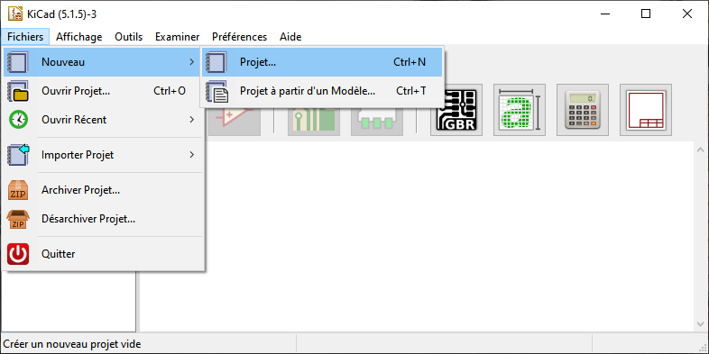
I create a new project
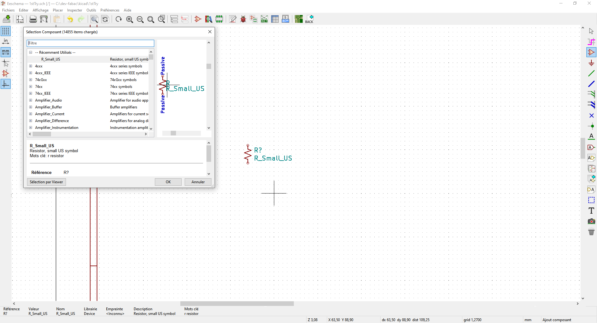
I add symbols
I can rotate symbol by press “R”. I place a wire by pressing this button.

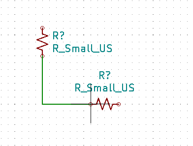
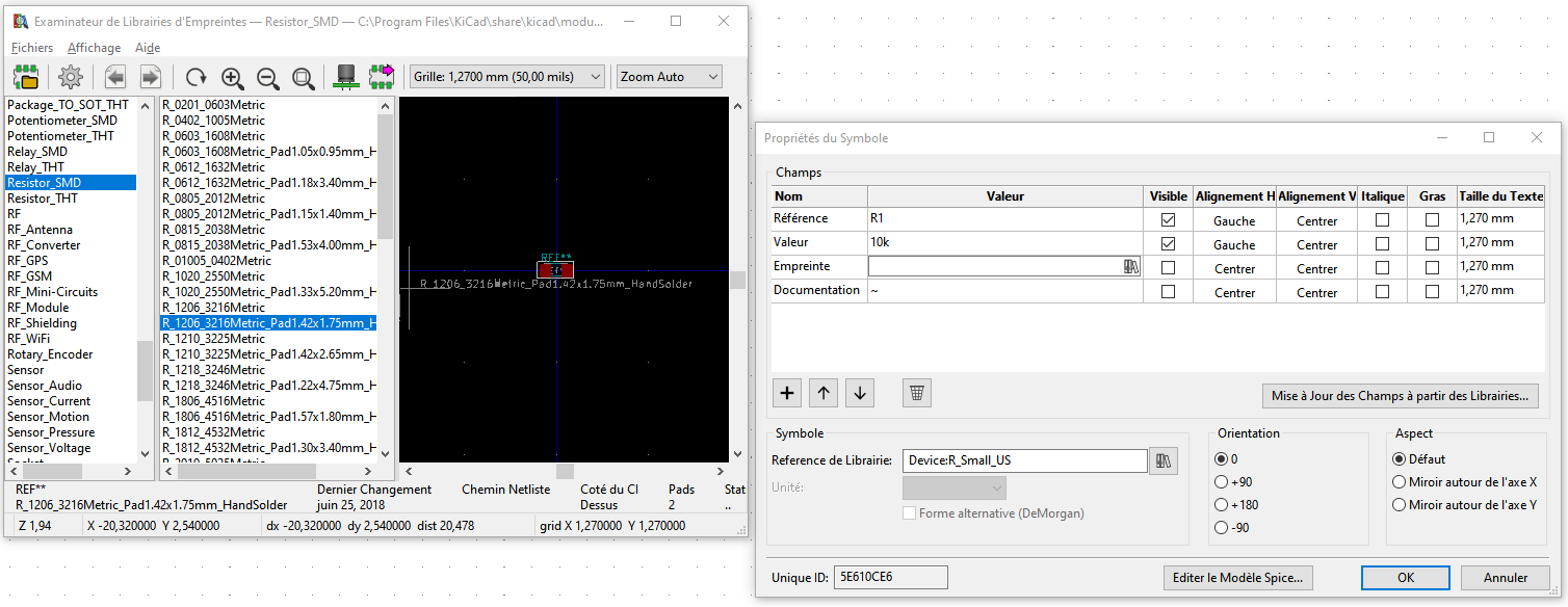
I can edit symbol properties by right clicking on it.
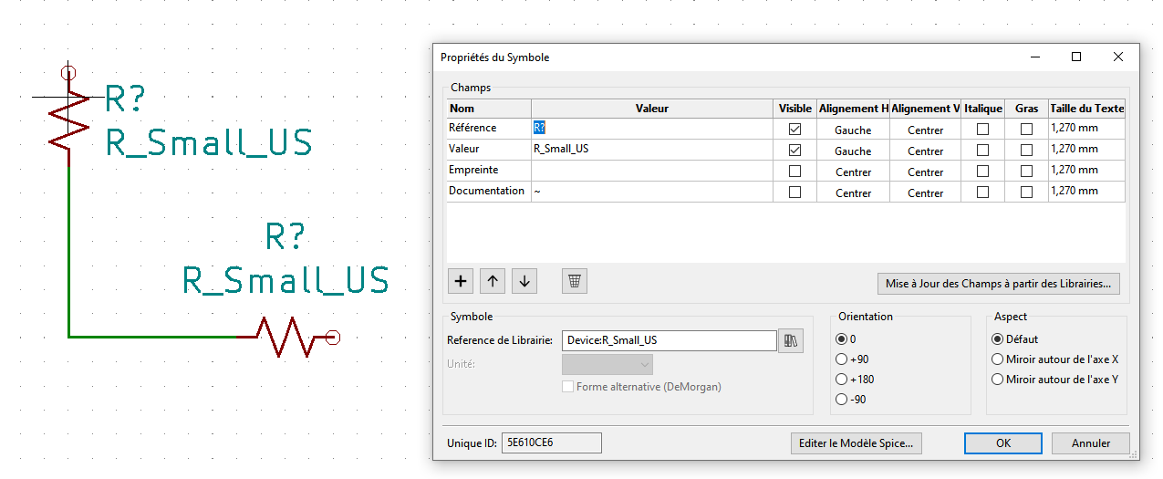
And setting footprint
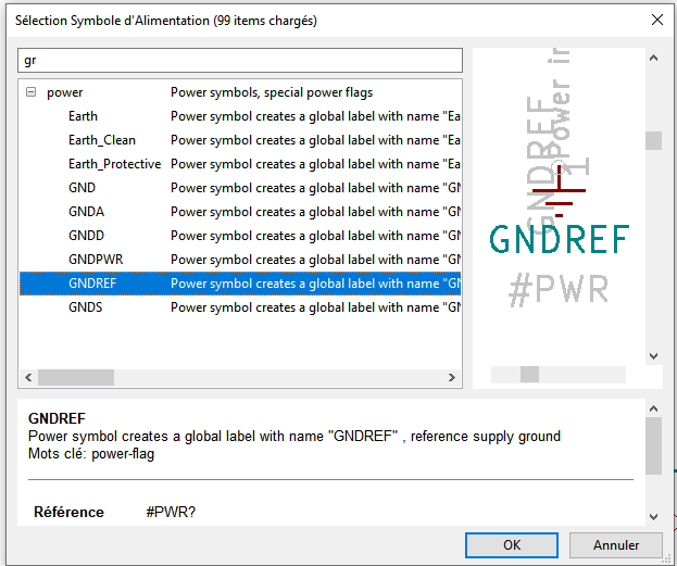
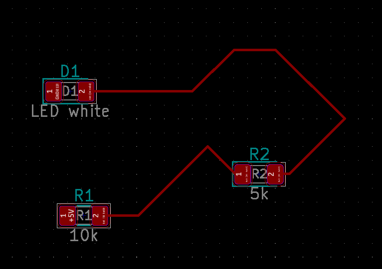
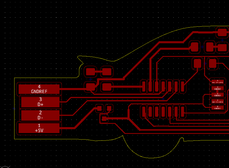
I add a LED and then a ground ref
Then a +5v and I wire all.
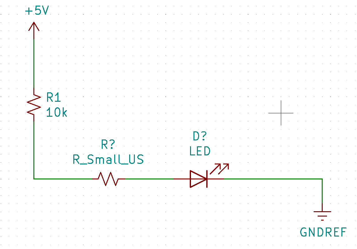
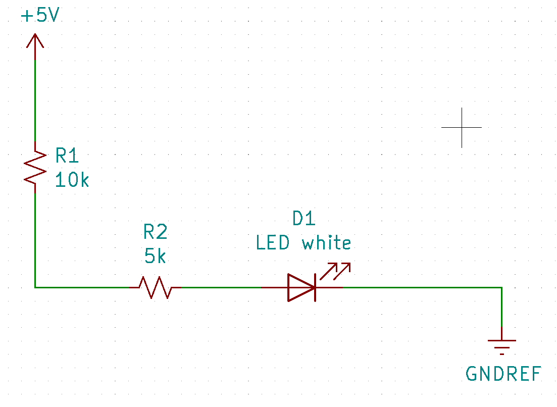
And also settings other components properties (name, footprint, value) and here the result :
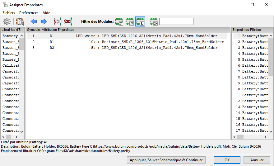
Then I verify footprints
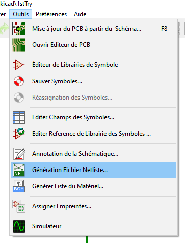
Then I generate NetList file
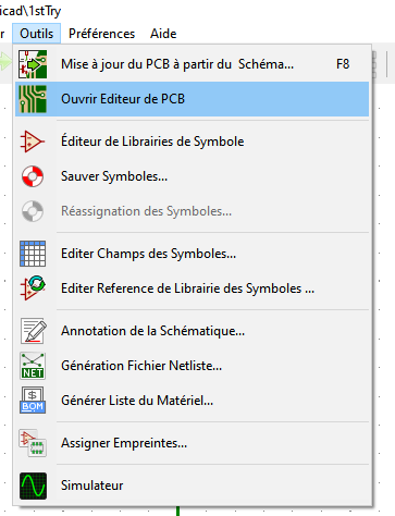
Then I go to PCB editor
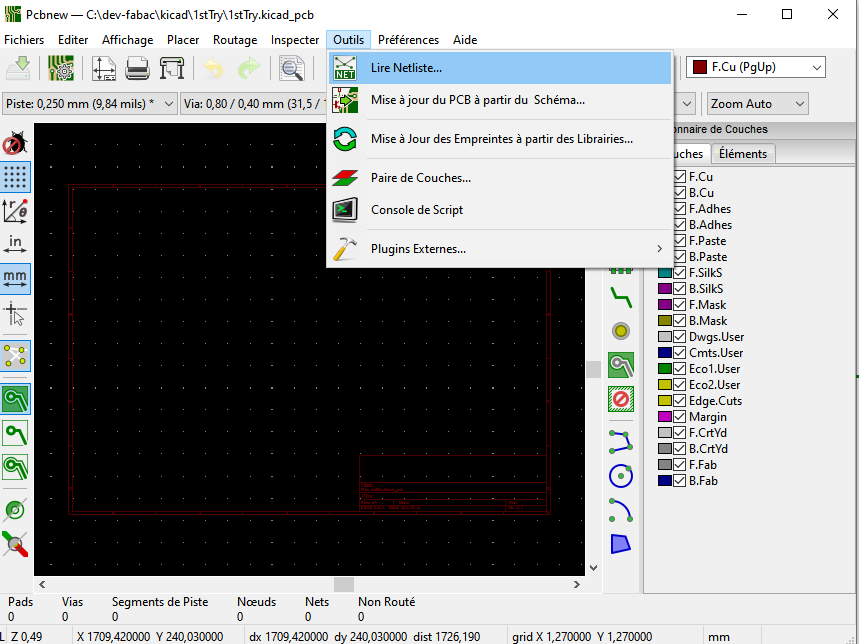
And I open NetList previously generated
And I update PCB and then close.
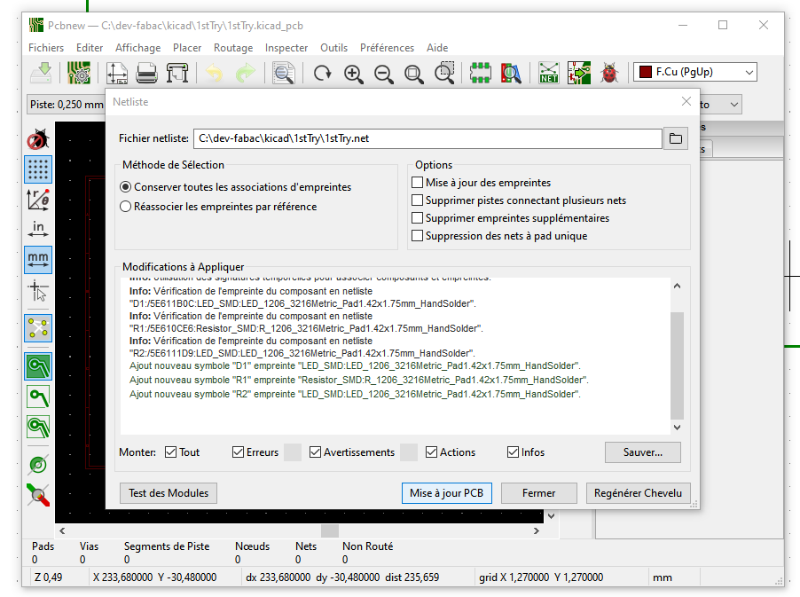
And I have my components on the PCB. Because I haven’t set footprint for +5V and GND REF, I have only my components.
I place them and put beautiful wires ^^
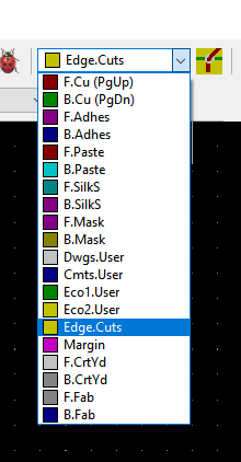
I switch Edge.Cuts Layer
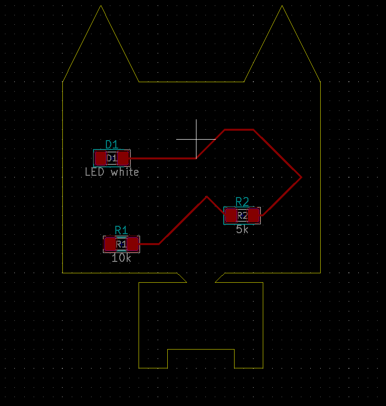
And I draw a lovely board
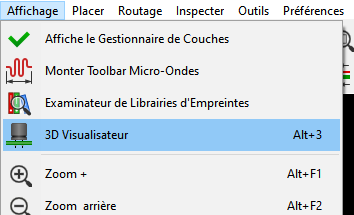
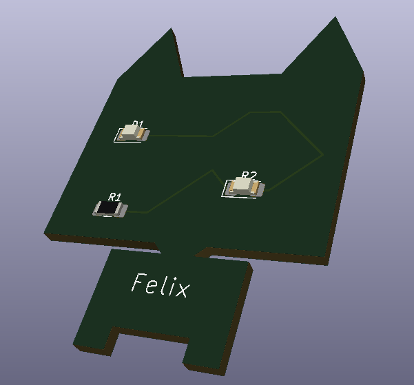
And I open 3d view
So beautiful !
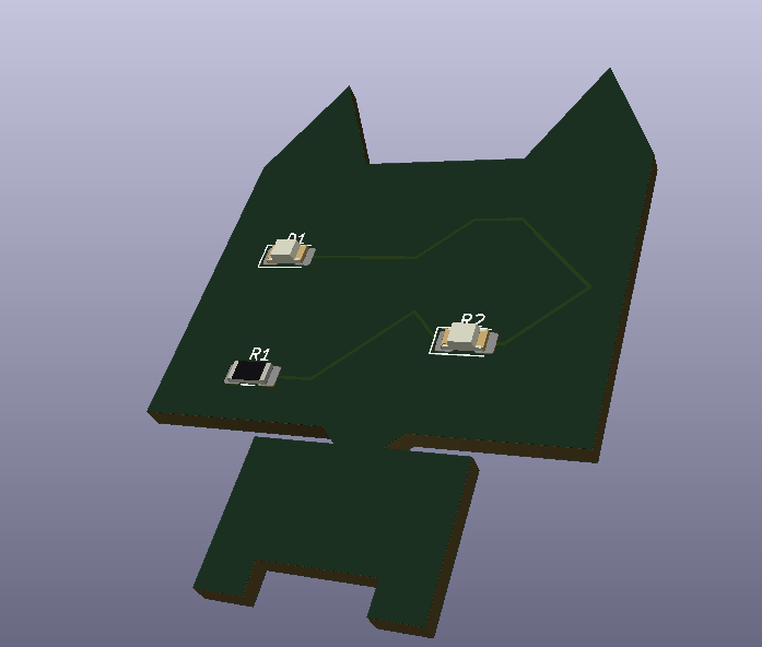
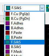
And I go to silk layer
And add some text
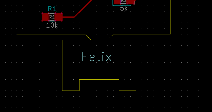
And now I have felix the cat’s board
Create my real board for this week
Drawing
I start by adding libraries in kicad https://forum.digikey.com/t/importing-the-digi-key-kicad-library-into-kicad-5-0-0/4075
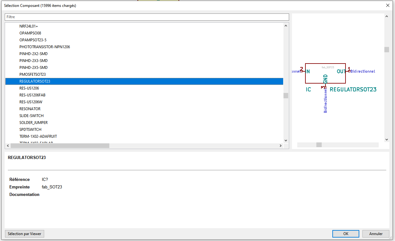
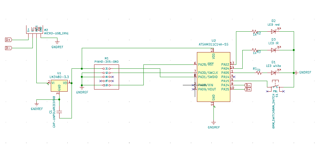
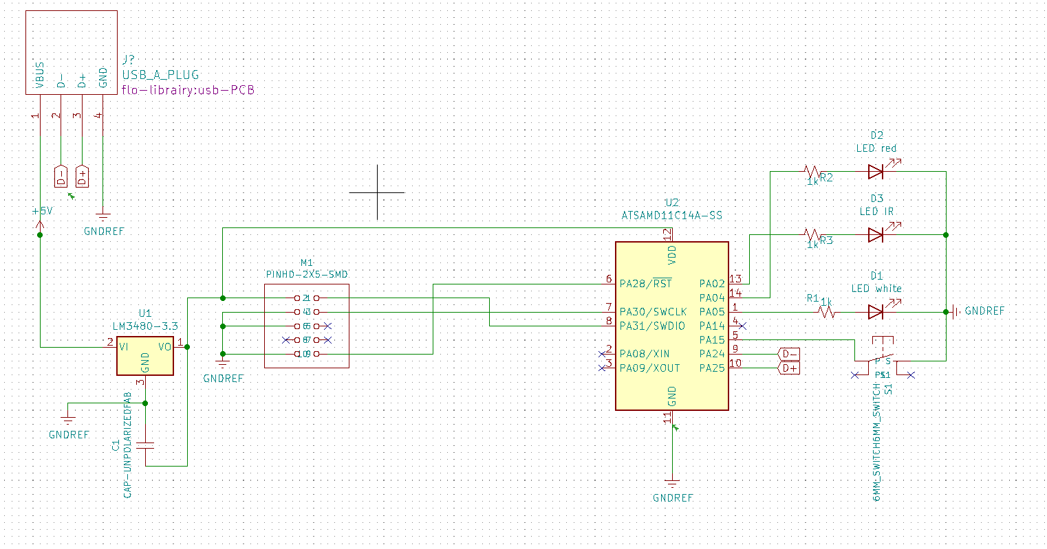
For my board, I need a SAMD11C
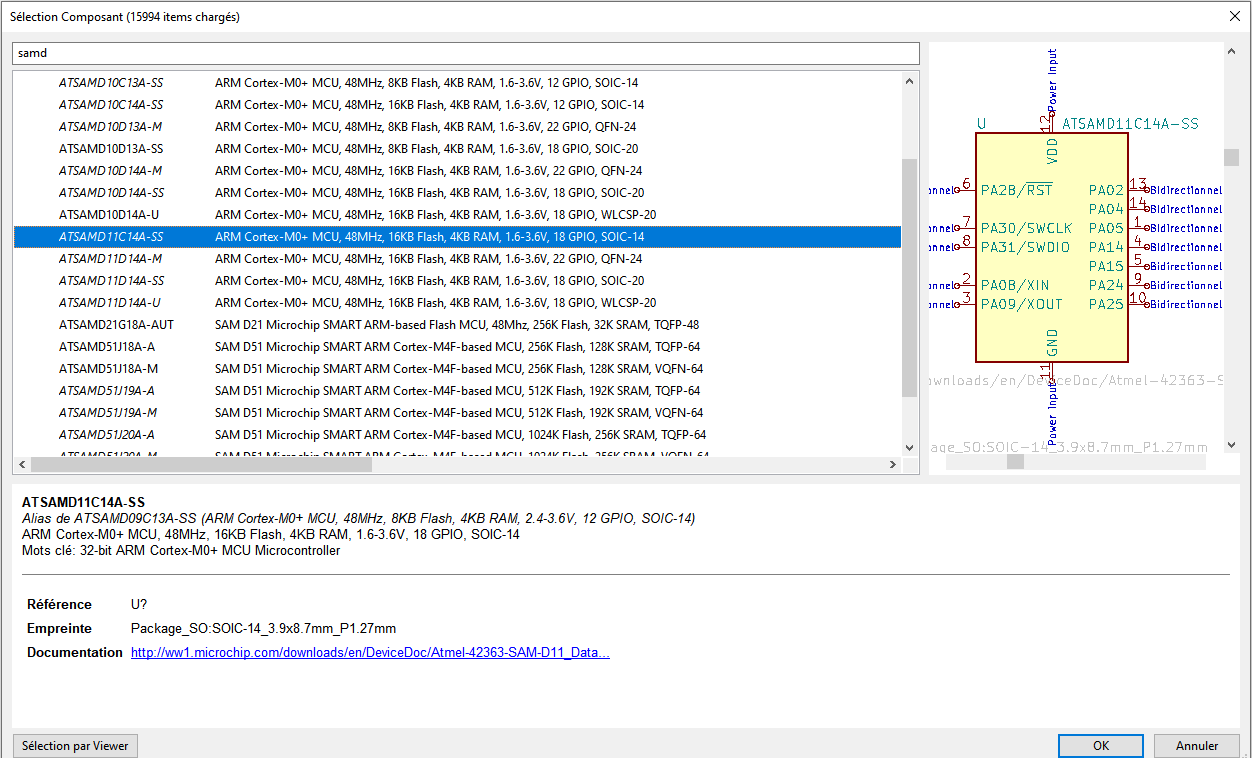
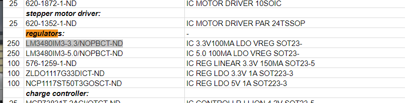
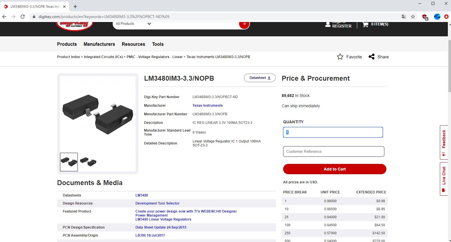
I verify if the component is in the inventory
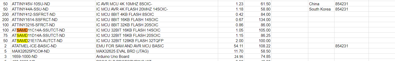
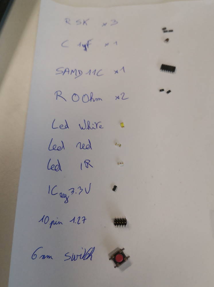
For building the board, I need to find good component, so I find them in inventory.
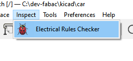
When making my board, I use “electrical rules checker”
I have severals warning for non connected PIN on some components, for reduce them I place “no connection flags” where I’m sure to connect nothing
Here the result at this time
I still have 2 remaining defauts but it’s more a bug than a real defaut
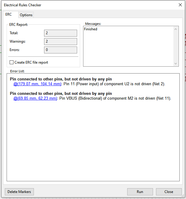
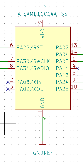
All my pins are connected but sometimes it says it’s not connected or not driven. For example, the PIN11 is the ground and it’s already connected to… ground
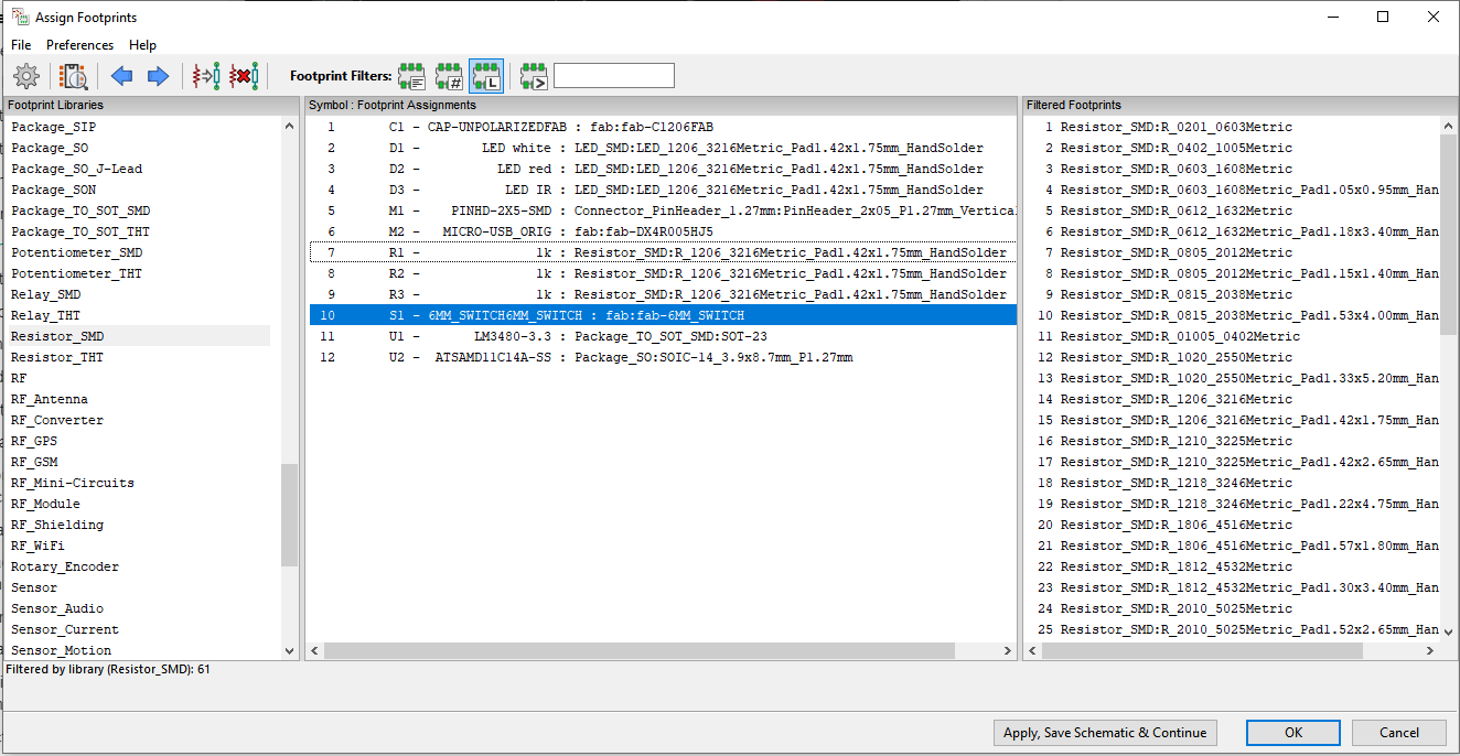
I have problem when assigning footprints, some components in fab librairy haven’t footprints, I have to assign footprint manually.
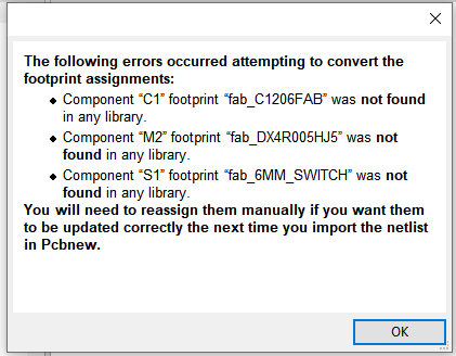
I assign footprints
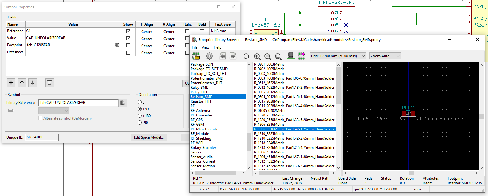
I try remove and reimporting fab librairies, still the problem. Finally I manually assign component and it seems ok.
After i select “update PCB from schematics” and I go to PCBnew
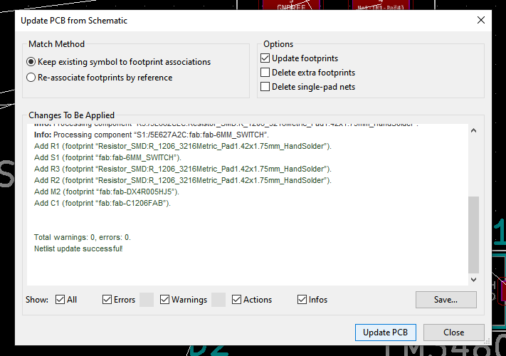
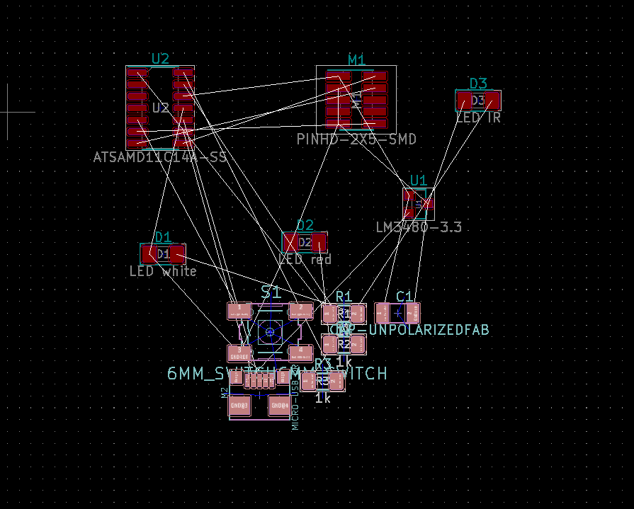
I click and I finally have all my components
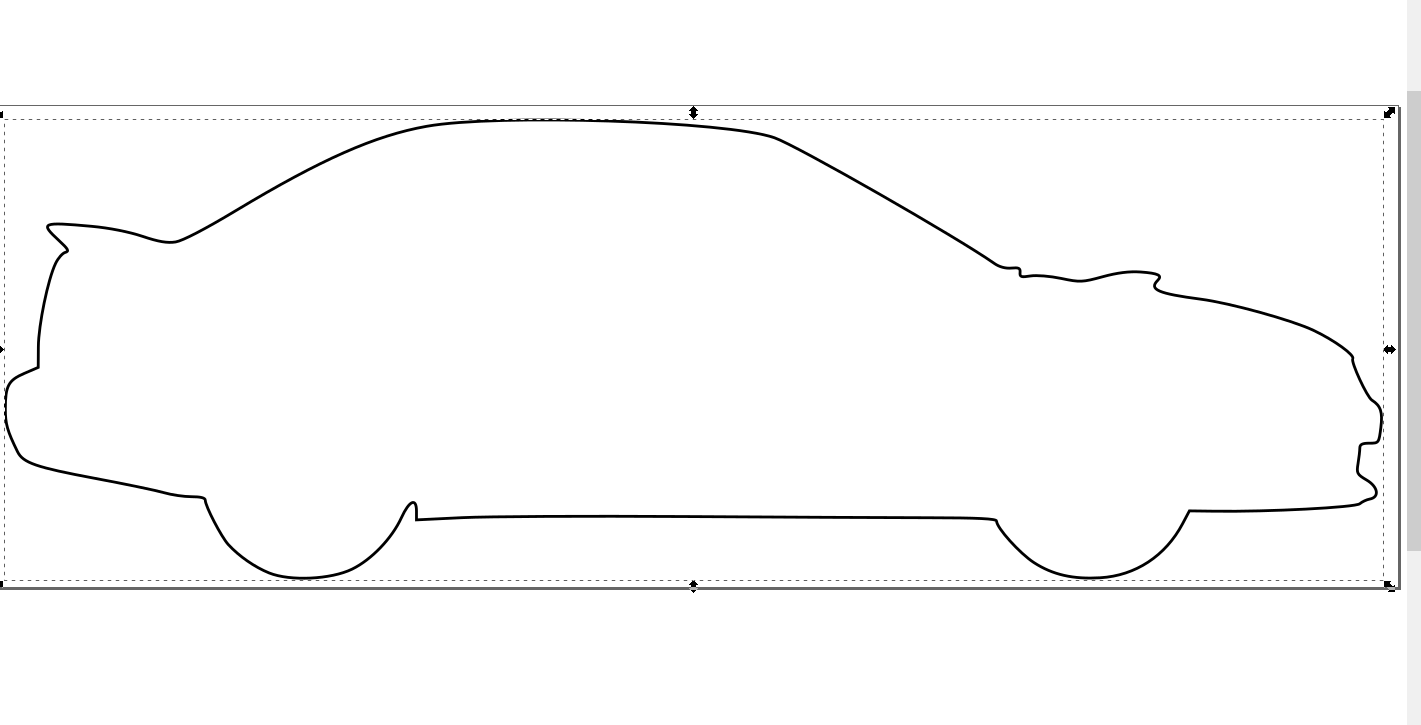
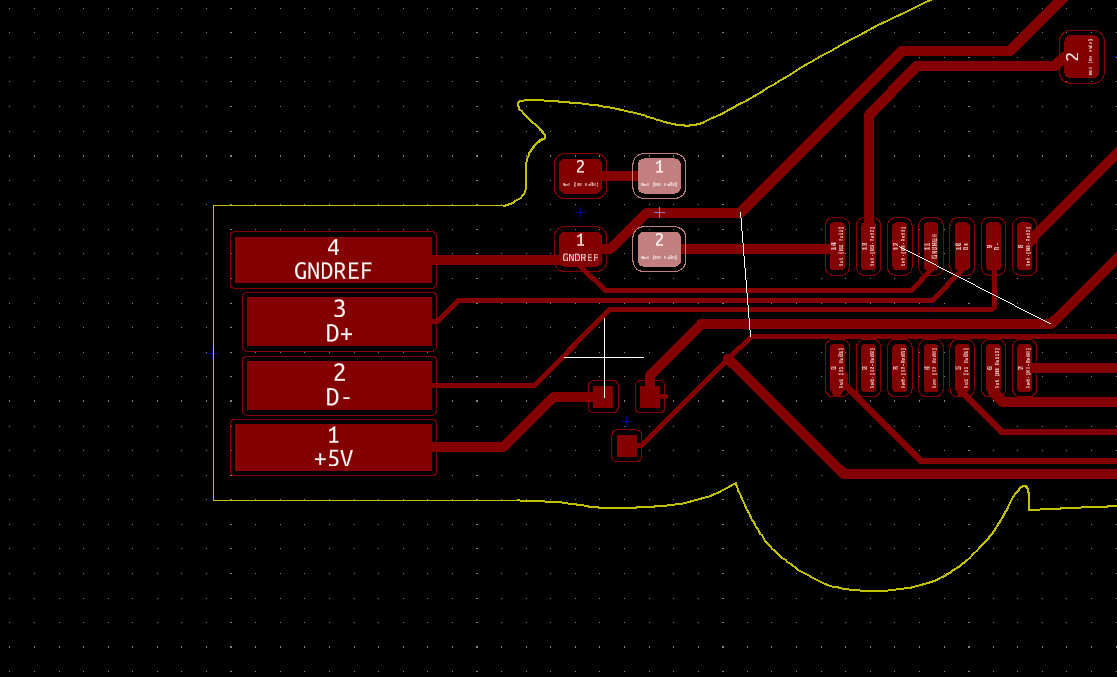
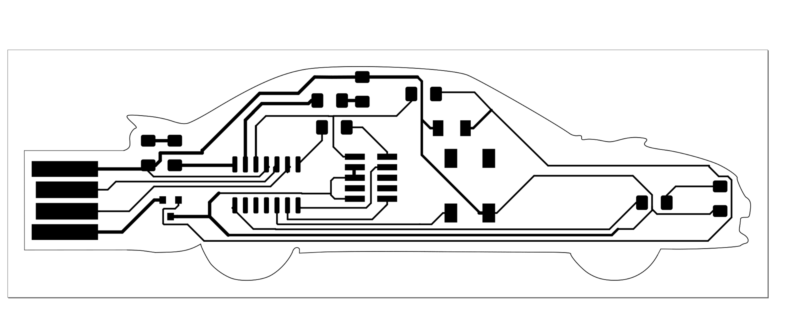
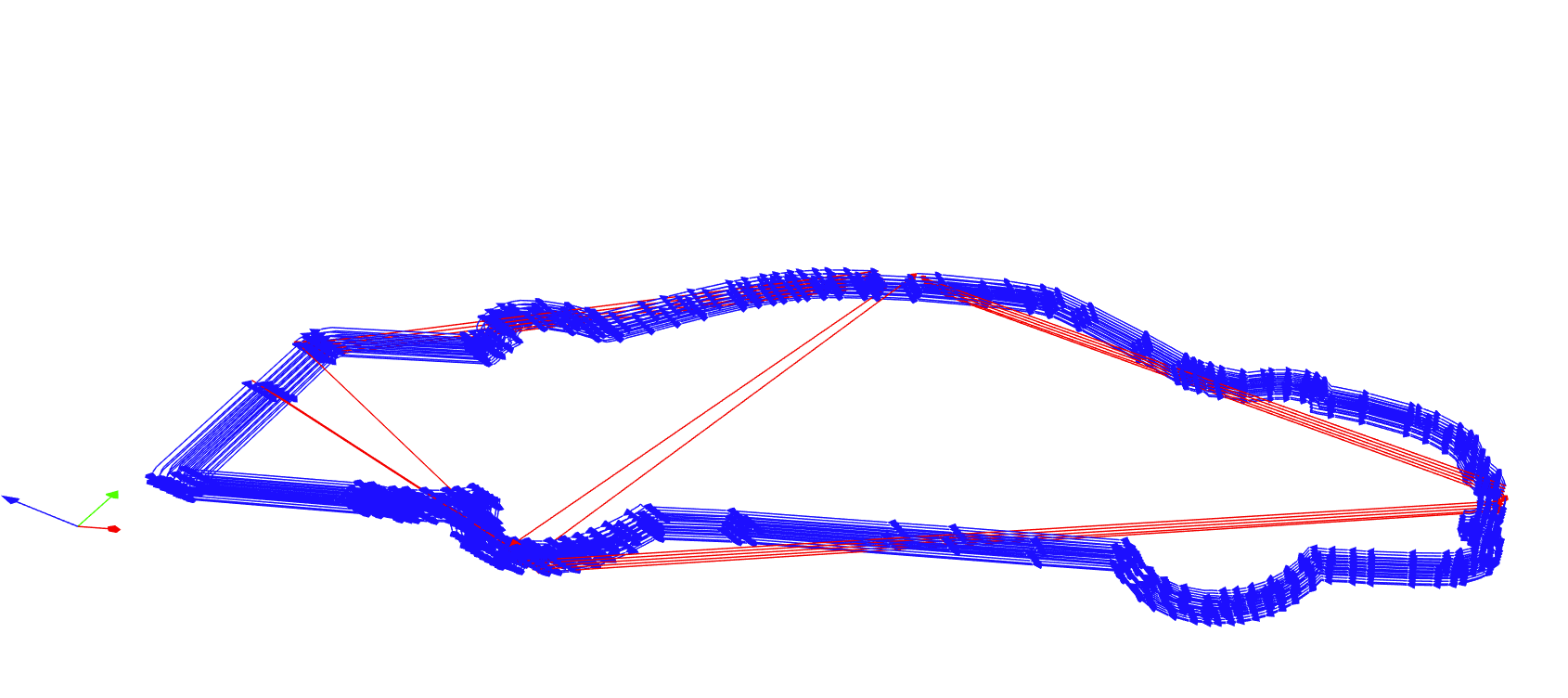
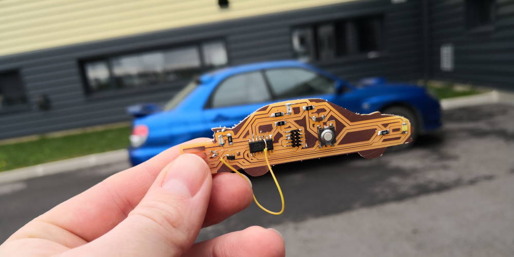
For the cutting, I’ve made my own profile of one of my car, a Subaru WRX 06
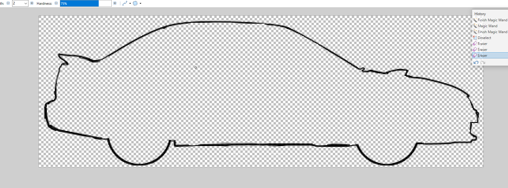
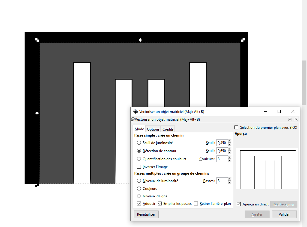
I vectorize in Inscape
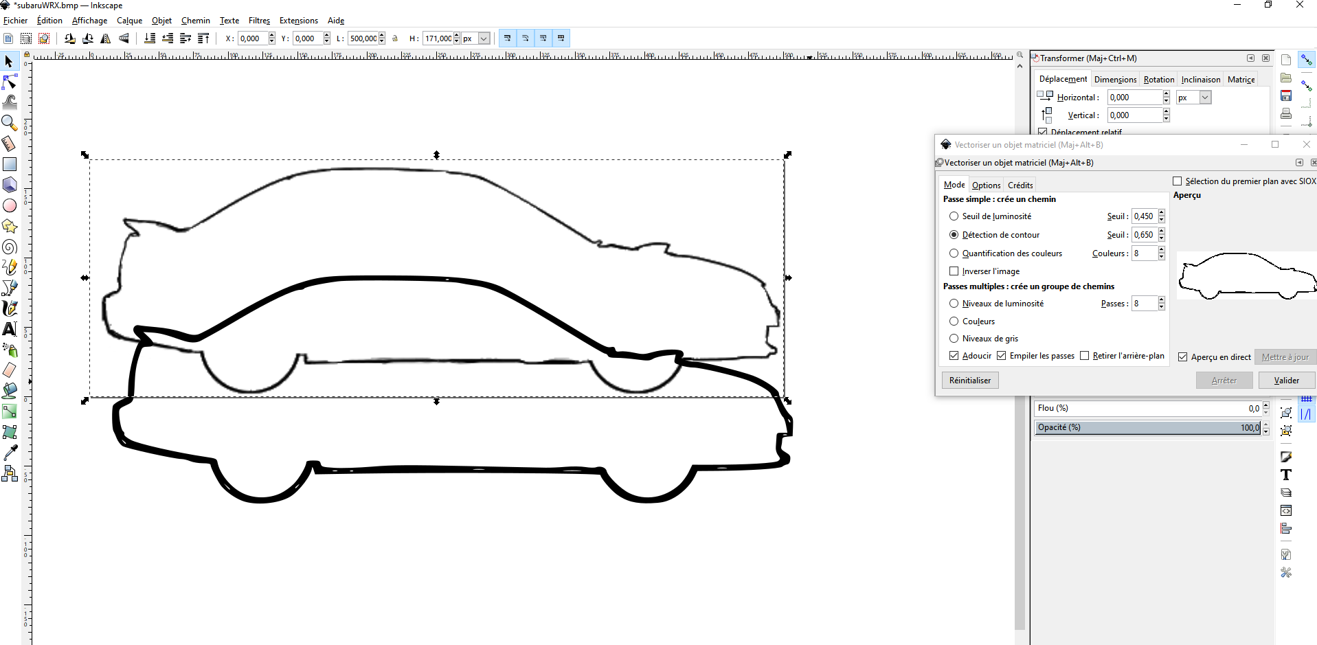 I clean the vectors to avoid double line and artefacts
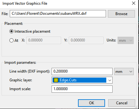
Save in dxf format and import in layer “Edge.Cuts” in PCBnew.
I haven’t found any footprint for an USB port integrated on the PCB like example on week05 so I use the traces in PNG, I put layers on Paint.net with transparency then I merge them.
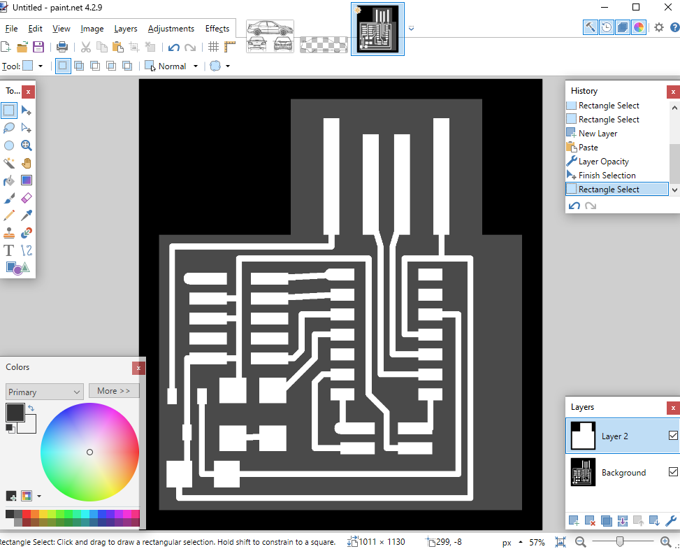
With Inkscape, I transform in vector
And now for the world premiere, the SubarUSB :)
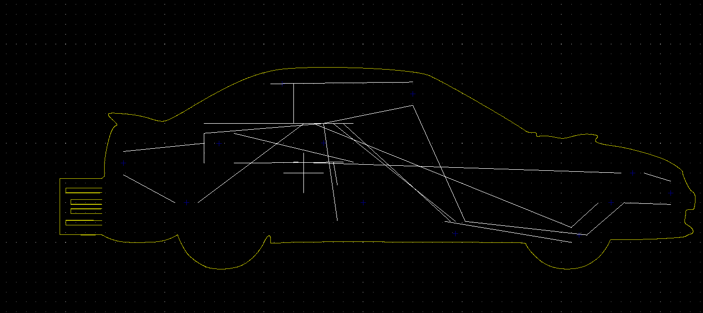
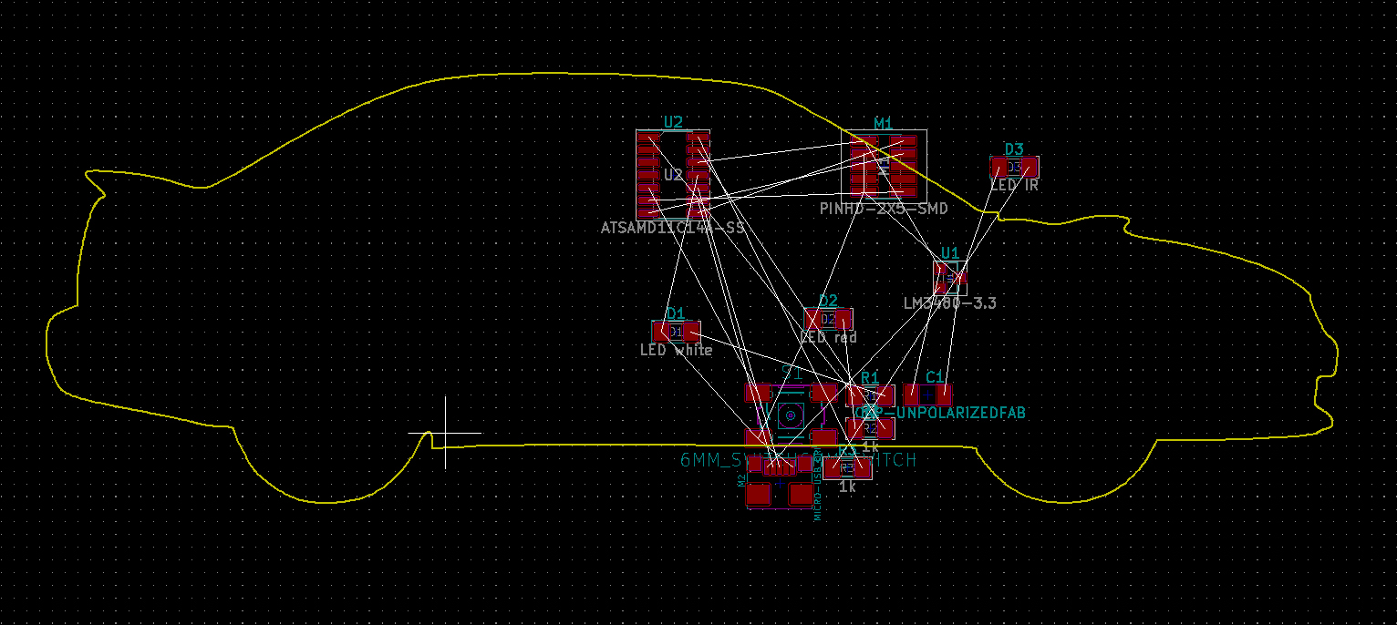
I have now to make all the traces inside this design.
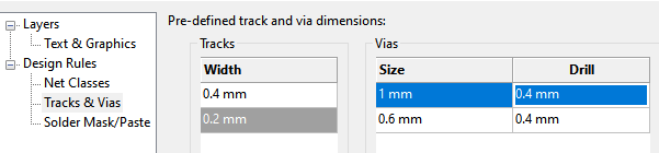
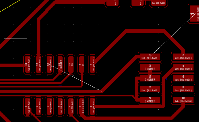
With help of CNC board of previous week. I choose 0.4mm for tracks and 0.2 mm if I have to make mini track. I also define vias even if I won’t use them this week (maybe later ^^).
I use “route track” to design tracks of my board.
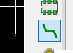
I have problem with USB connector, I don’t want to draw it manually in the SVG output so I finish after hours or searching.
I found this page https://forum.kicad.info/t/standard-github-usb-trace-on-pcb-footprint-available/1800/6
I download Board shematics and layout here
I open the project on KiCAD
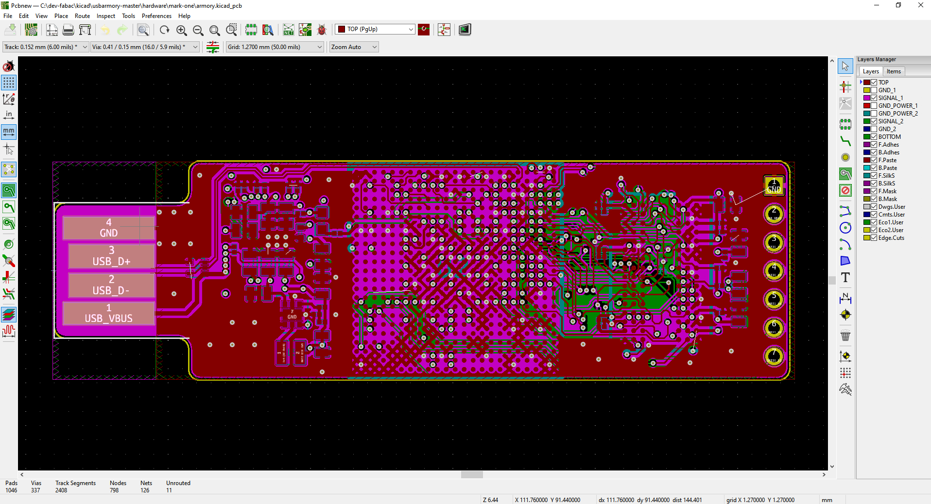
I extract the footprint of the PCB/USB plug and I import it on my own KiCAD library.
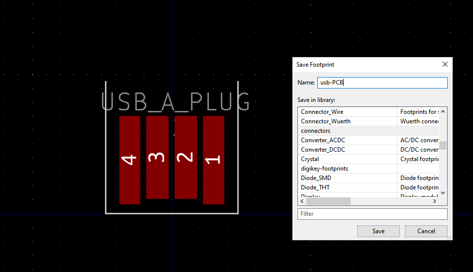
So I modify my schematic and replace with an USB A plug
And I will plug with the new footprint I got :)
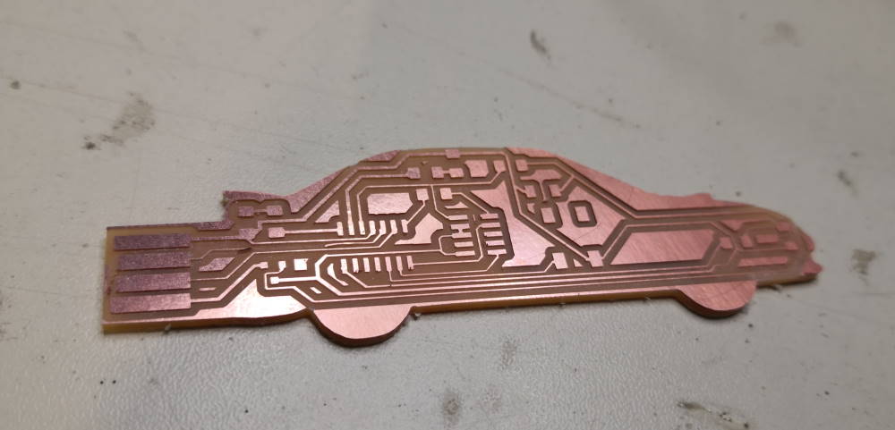
On the updated PCB with the correct footprint I see my USB port is wrong. So I have to redraw the rear USBumper of the car.
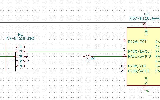
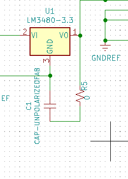
I see I need a bridge, so I add a 0 resistor to pass over a trace.
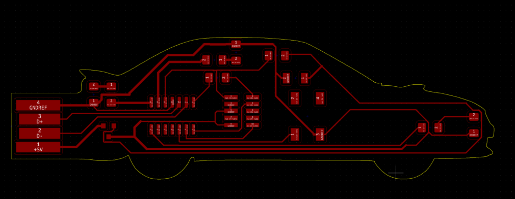
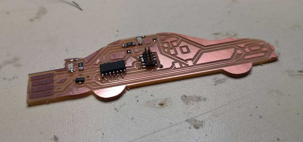
And now all the board is wired.
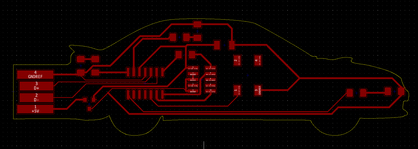
I export F.Cu and Edge.Cut layers in svg
I go to mods, I select SRM20 > svg file. I import, I put my setting and … noooo
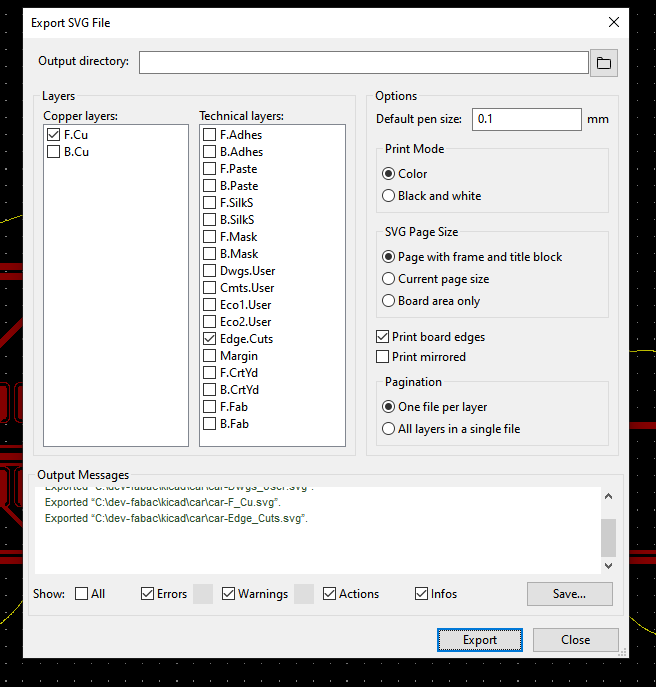
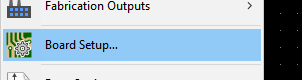
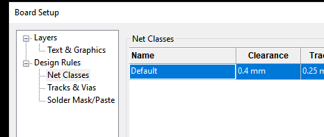
Some of my routes are not correctly cut, clearance is wrong. So I need to modify my design rules. It’s in File > Board Setup…
And I modify clearance to be 0.4 mm (the mill size obviously)
And I run design rules checker to verify all my board
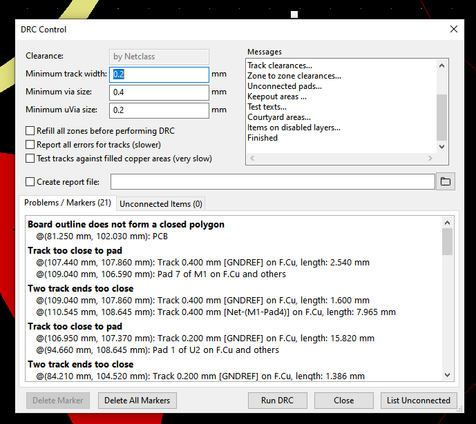
Clearance problems… I can’t put more than 4 traces under the SAMD11C with 0.4mm of clearance
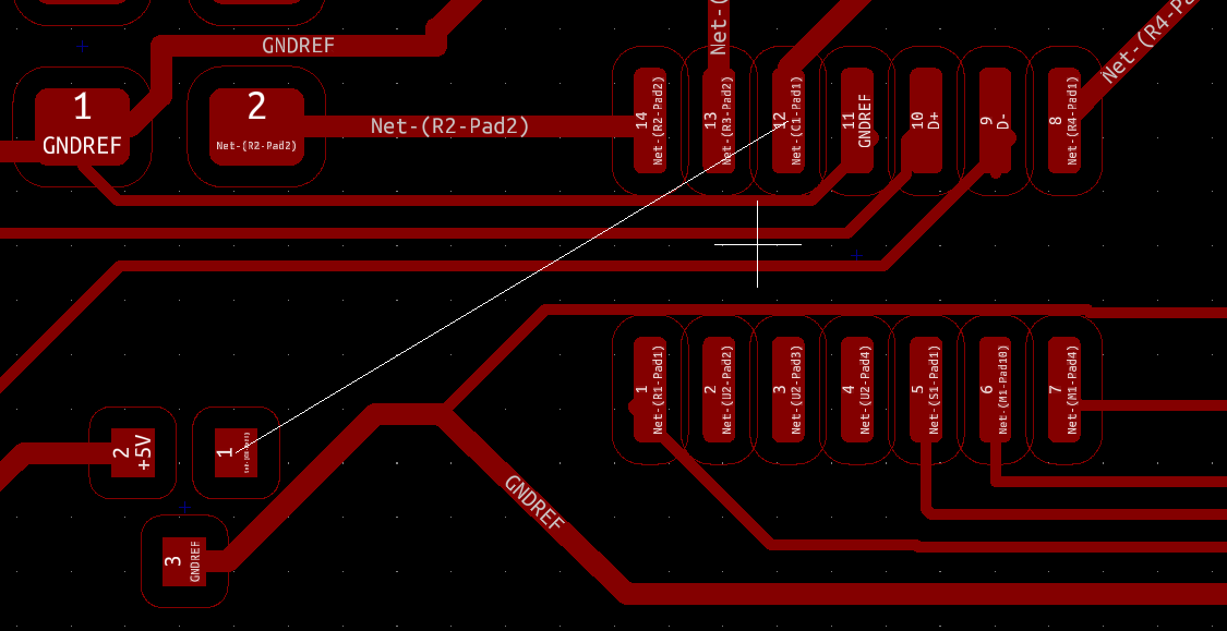
I have to find a way to put my trace. I put another 0 resistor to make another bridge. Slightly modify design of the board, playing with different trace width.
Finally after many try and retry and retry and redesign, the final version. I have to move the +3.3V all around the board and then I can bridge over 1 trace. If I use vias, circuit will be more easy to design.
I have my 3 LED, my button, Let’s go back to mod and verify if all it’s ok.
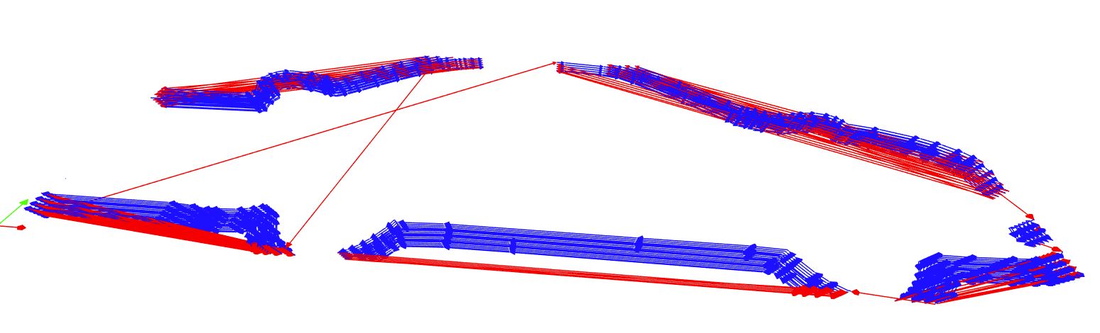
A quick 3D view
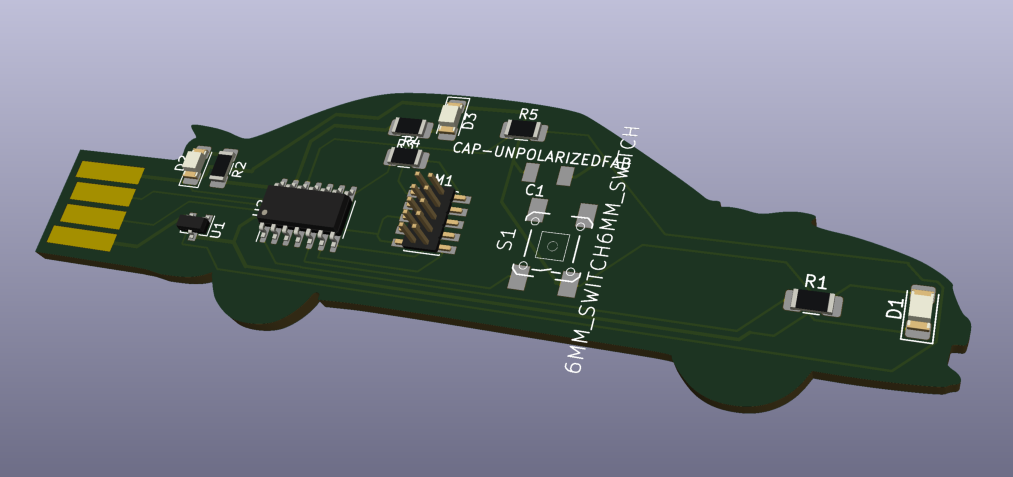
I haven’t all components in 3D but it’s great. I generate files in svg. I put in mods the traces in F.Cu. All Good.
Here all the settings I use like in week05.
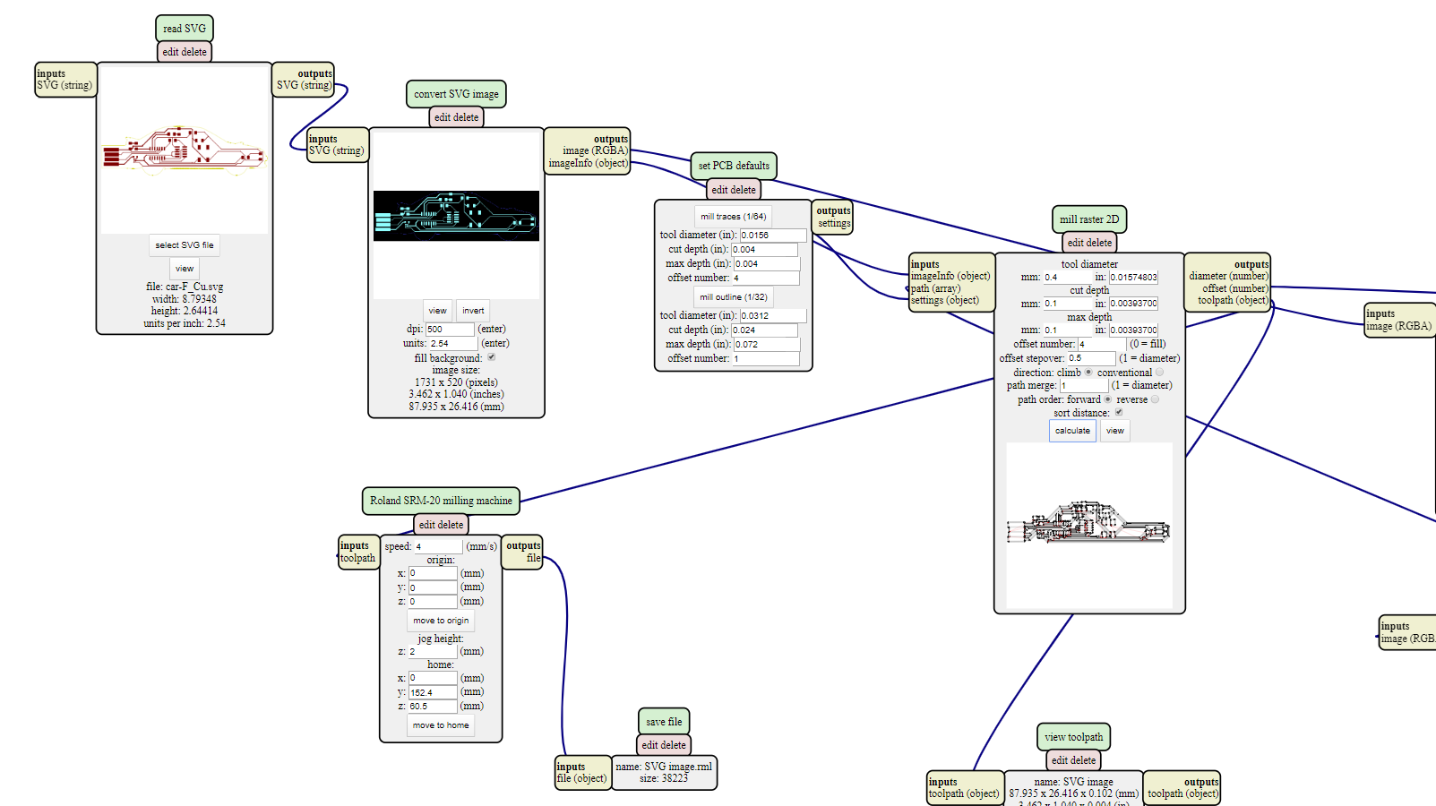
“Invert image” in convert module. Mill diameter 0.4mm, cut depth & max depth 0.1mm, speed 4mm/s, x&y&z @ 0, change output to “file>save” module.
Cut lines don’t works in mods. I use Inkscape to open svg and fill the board with black.

Then I go back to mods and it’s works.
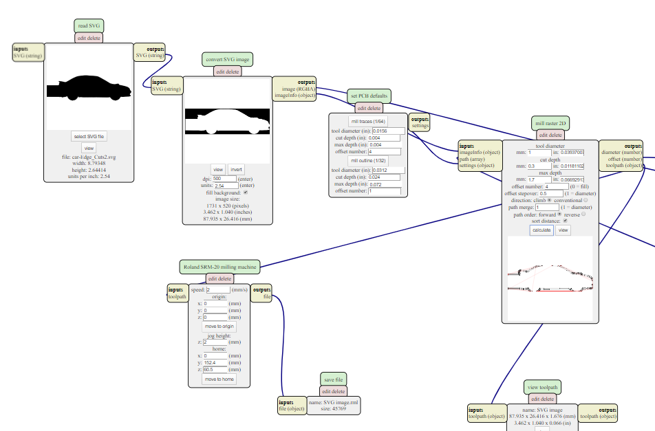
Settings applied : “Invert image” in convert module. Mill diameter 1mm, cut depth 0.3mm, max depth 1.7 mm (a board is 1.5mm thick), speed 2mm/s, x&y&z @ 0, change output to “file>save” module.
But when I verify mill path, I see it’s not gonna pass everywhere around my board. Why? It’s seems it’s also need “clearance” in my image to have milling going on all edges.
To bypass this problem, I export my 2 layers in one file. I modify marging by adding 2mm on each side. And then I export 2 different files I can import in mod and keep same reference.

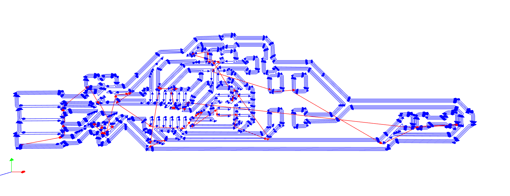
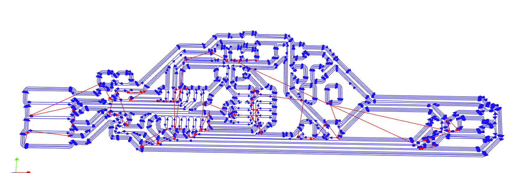
And now mill path looks good in mods.
MILLING part 1
I’ve got some problems when milling.
1/ 0.4 mill breaks, first time for me, I reuse a old mill, maybe it had a problem in previous milling. I don’t know.
2/ I change for a new 0.4mm mill, all is fine. To be secure, I go at 80% speed. But when looking at the end, one of my track was broken when milling. Only one even if I made many 0.2mm width traces, I have the problem on only one.
3/ When milling outer edges with 1mm mill, it takes very long time. I see that mods generate many traces. So I stop before the end because it has already finish completely one turn.
REWORK
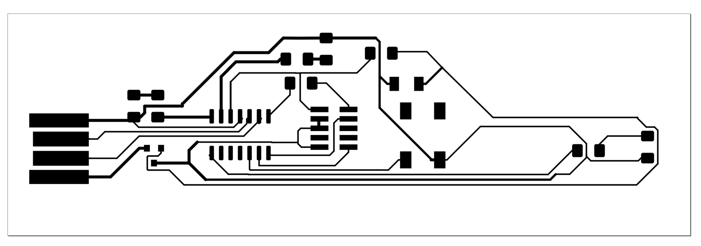
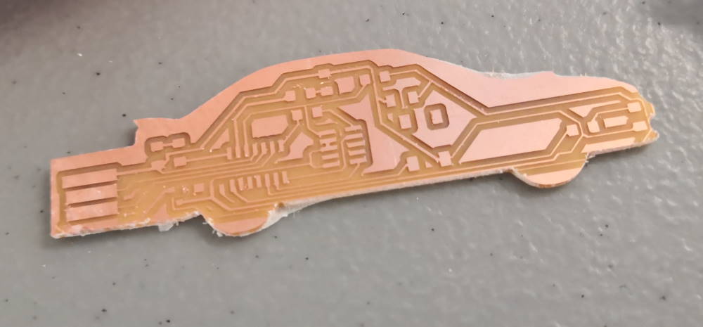
Because I don’t want to put wire (it’s soooo bad) I try rework on faulty track. I remove all traces in the zone and put new ones with 0.25mm width, only one remains in 0.2mm because of lack of space (fingers crossed).
I’ve to redo all transform steps (open in inkscape, create 2 separate layers with correct margin) of course but it’s the game, the show must go on.
Problem is in inkscape, the car shape and the usb port are exported in 2 different objects. I combine them in inkscape and have to use fill tool but it appears it doesn’t fill correctly, I can’t just add black blackground because combined objet may be not fullu close. No solution yet so I keep this barely shape by destroying initial shape.

I’ve still got problem, finally I found!!!
I have forgotten to put offset at 1!!!
MILLING PART 2
I launch another milling, traces was OK. But when I launch EDGES, it was a problem with the offset and board was failed.
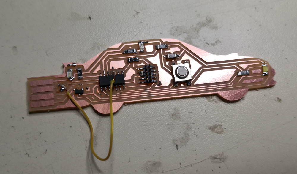
No time for verify all and launch a 3rd board, I’ll take the first and add an ugly wire.
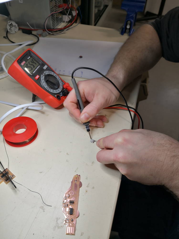
In the meantime, I prepare components (finally I take another button that fit better)
Soldering in progress
The board finished (with the wire of shame).
Flashing & little dev
Let’s go to flash. After installing all Atmel drivers for the flash box. Plug the board, green LED. YES!!!
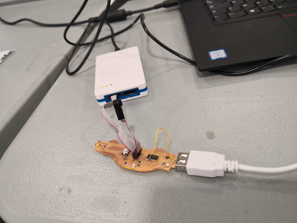
First I have to flash the booloader.
ebdg.exe -b -t samd11 -pv -f sam_ba_Generic_D11C14A_SAMD11C14A.bin
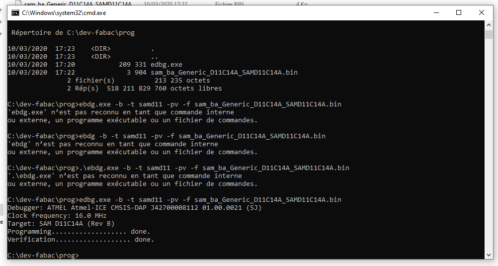
Flash successful! Programmer can be removed because it’s not needed anymore. You can program the board directly with the USB port.
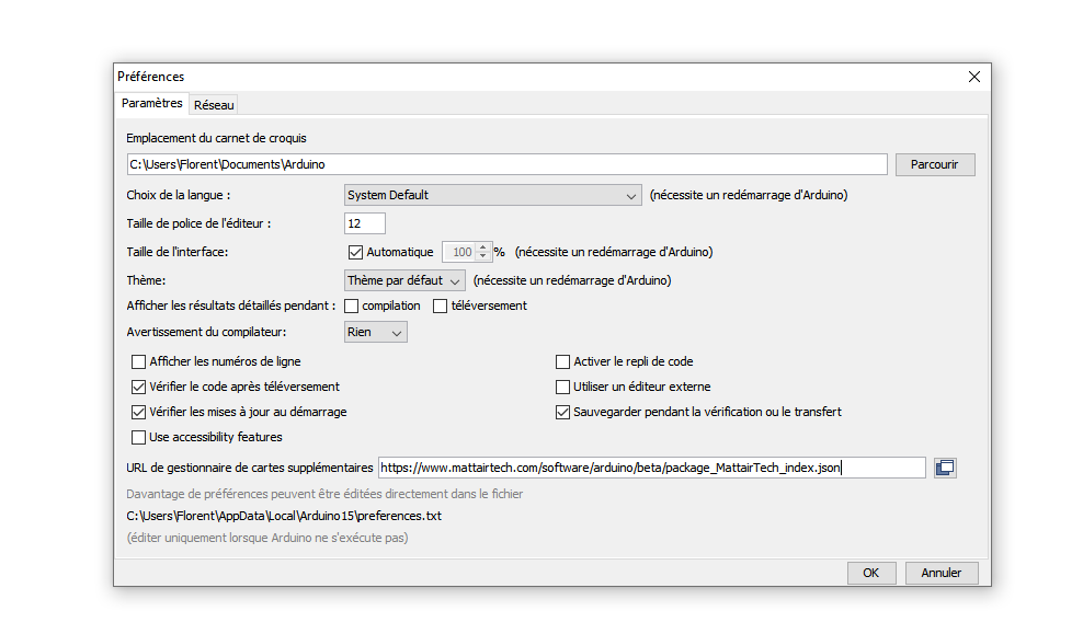
I use the arduino software. You have to install the boards, first add a new URL in arduino software for boards : https://www.mattairtech.com/software/arduino/beta/package_MattairTech_index.json
Now I can install “MattairTech SAM D|L|C core for arduino”.
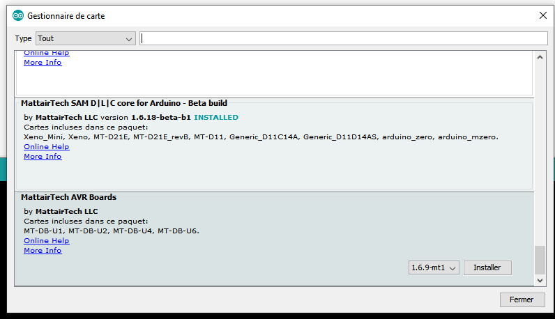
Correct board doesn’t appear yet. You to go one more time to board manager, see update available et update “MattairTech SAM D|L|C core for arduino” in a beta version (here 1.6.18-beta-b1).
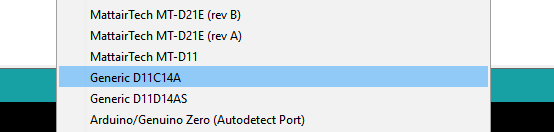
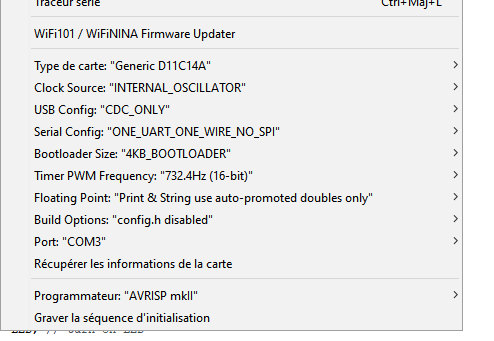
Now you can set the correct board Generic D11C114A
Here my setting before flashing the board with arduino.
I first test the Neil code that blink one of my LED. Then I start from the blink arduino example and referring to the pin I plug my white and red LED, I do my own code :
// the setup function runs once when you press reset or power the board
void setup() {
  // initialize my two led pin as output.
  pinMode(5, OUTPUT);
  pinMode(4, OUTPUT);
}

// the loop function runs over and over again forever
void loop() {
  digitalWrite(5, HIGH);
  digitalWrite(4, HIGH);// turn the LED on (HIGH is the voltage level)
  delay(1000);                       // wait for a second
  digitalWrite(5, LOW);
  digitalWrite(4, LOW);// turn the LED off by making the voltage LOW
  delay(1000);                       // wait for a second
}
Then I flash my board.
Le croquis utilise 9400 octets (76%) de l'espace de stockage de programmes. Le maximum est de 12288 octets.
Atmel SMART device 0x10030006 found
Device       : ATSAMD11C14A
Chip ID      : 10030006
Version      : v2.0 Nov 22 2017 12:56:25
Address      : 4096
Pages        : 192
Page Size    : 64 bytes
Total Size   : 12KB
Planes       : 1
Lock Regions : 16
Locked       : none
Security     : false
Boot Flash   : true
BOD          : true
BOR          : true
Erase flash
done in 0.777 seconds

Write 9752 bytes to flash (153 pages)

[                              ] 0% (0/153 pages)
[==                            ] 9% (15/153 pages)
[=====                         ] 19% (30/153 pages)
[========                      ] 29% (45/153 pages)
[===========                   ] 39% (60/153 pages)
[==============                ] 49% (75/153 pages)
[=================             ] 58% (90/153 pages)
[====================          ] 68% (105/153 pages)
[=======================       ] 78% (120/153 pages)
[==========================    ] 88% (135/153 pages)
[============================= ] 98% (150/153 pages)
[==============================] 100% (153/153 pages)
done in 7.142 seconds

Verify 9752 bytes of flash

[                              ] 0% (0/153 pages)
[==                            ] 9% (15/153 pages)
[=====                         ] 19% (30/153 pages)
[========                      ] 29% (45/153 pages)
[===========                   ] 39% (60/153 pages)
[==============                ] 49% (75/153 pages)
[=================             ] 58% (90/153 pages)
[====================          ] 68% (105/153 pages)
[=======================       ] 78% (120/153 pages)
[==========================    ] 88% (135/153 pages)
[============================= ] 98% (150/153 pages)
[==============================] 100% (153/153 pages)
Verify successful
done in 0.059 seconds
CPU reset.
And voilà
GROUP ASSIGNEMENT
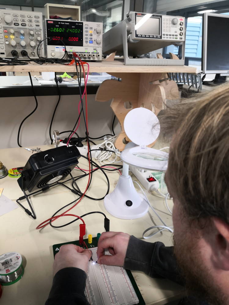
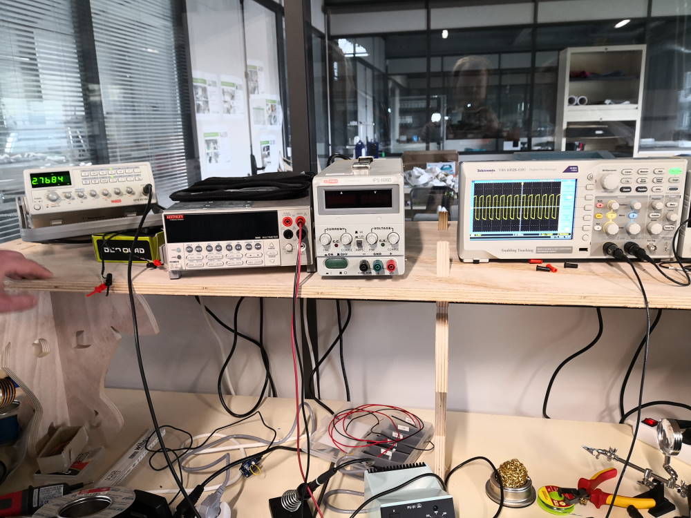
Using DC power supply to test LED polarity (with 2.6V)
Using multimeter to verify which group of 2 pins use on the button
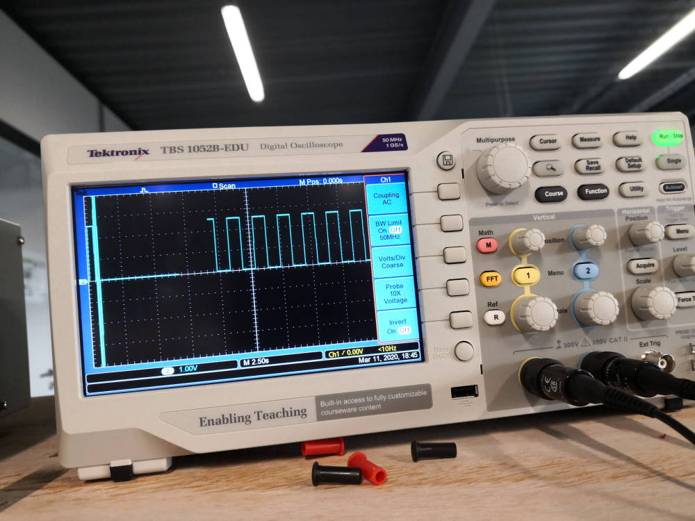
Using oscilloscope and frequency generator setting signal and reading it
Using oscilloscope to see frequency of my blink on my board (up 1s, down 1s)