Group assignment
- Characterize the design rules for your PCB production process
Workflow
The group members are Renzo, Silvia and I. The group assignment allows knowing the milling process, it was used the milling machine Roland Modela MDX40a and the online software mods as its controller.
Engraving (traces) and cutting (interior) PNG files were downloaded and then loaded into mods.
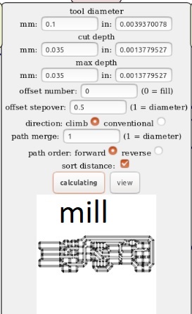
Then, for milling (and cutting too) you have to enter the parameters with which the milling machine will work (on mods).
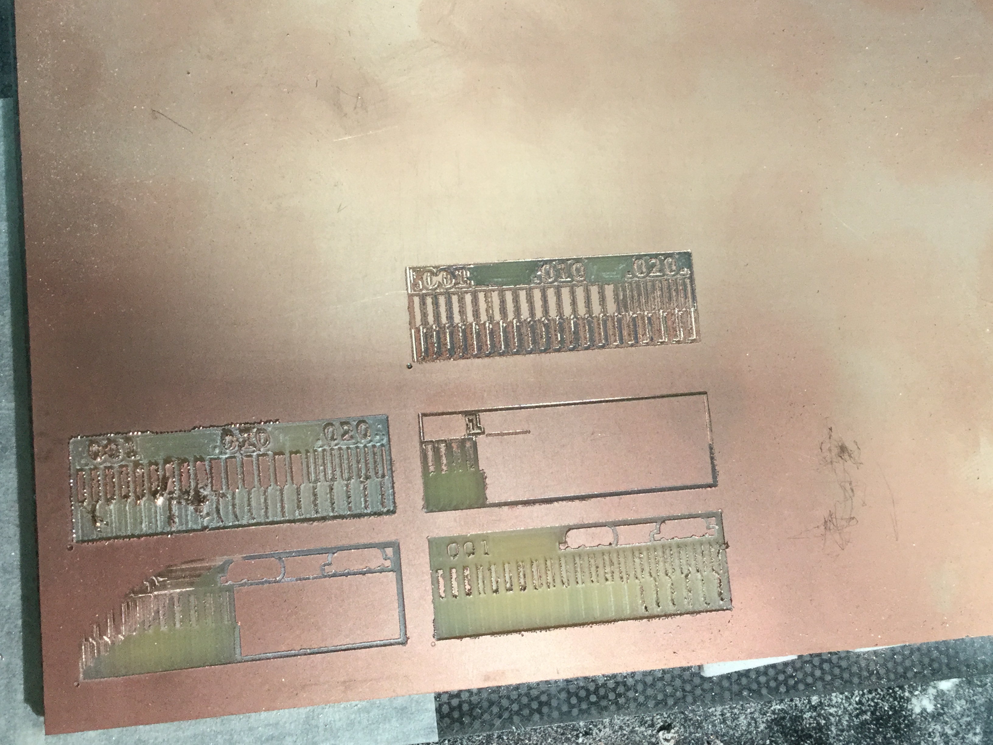
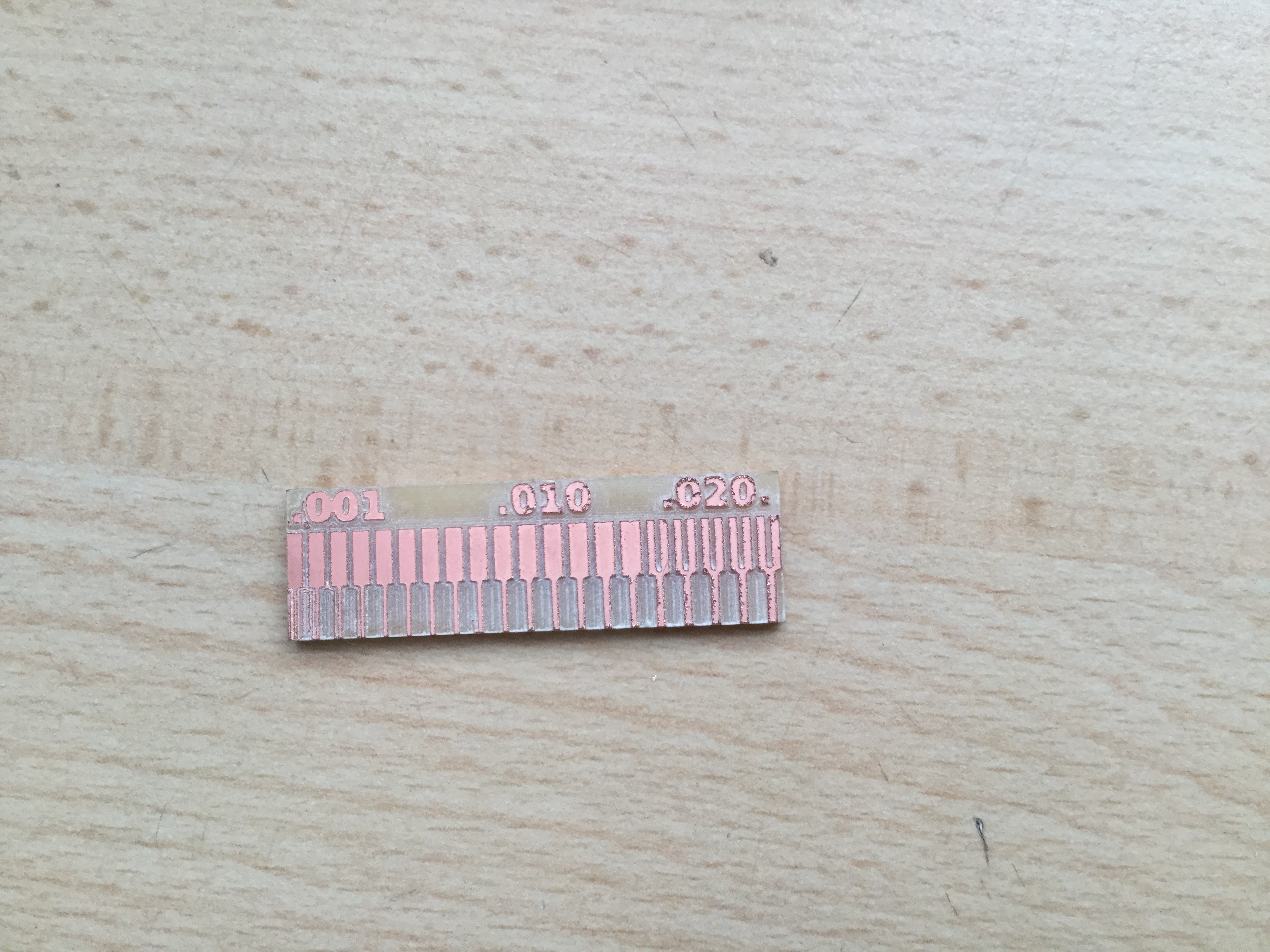
The parameters that must be entered are: diameter of the milling cutter (0.01 mm for milling and 1/32" for cutting), cut depth (here consider that the thickness of the copper layer must be traversed for milling, and for the cut through the Bakelite layer as well, so these thicknesses should be considered). With "offset number" indicates if you want to remove all excess copper or no (0 = remove all). The other parameters are related to the position of the geometrical cero of the mill.
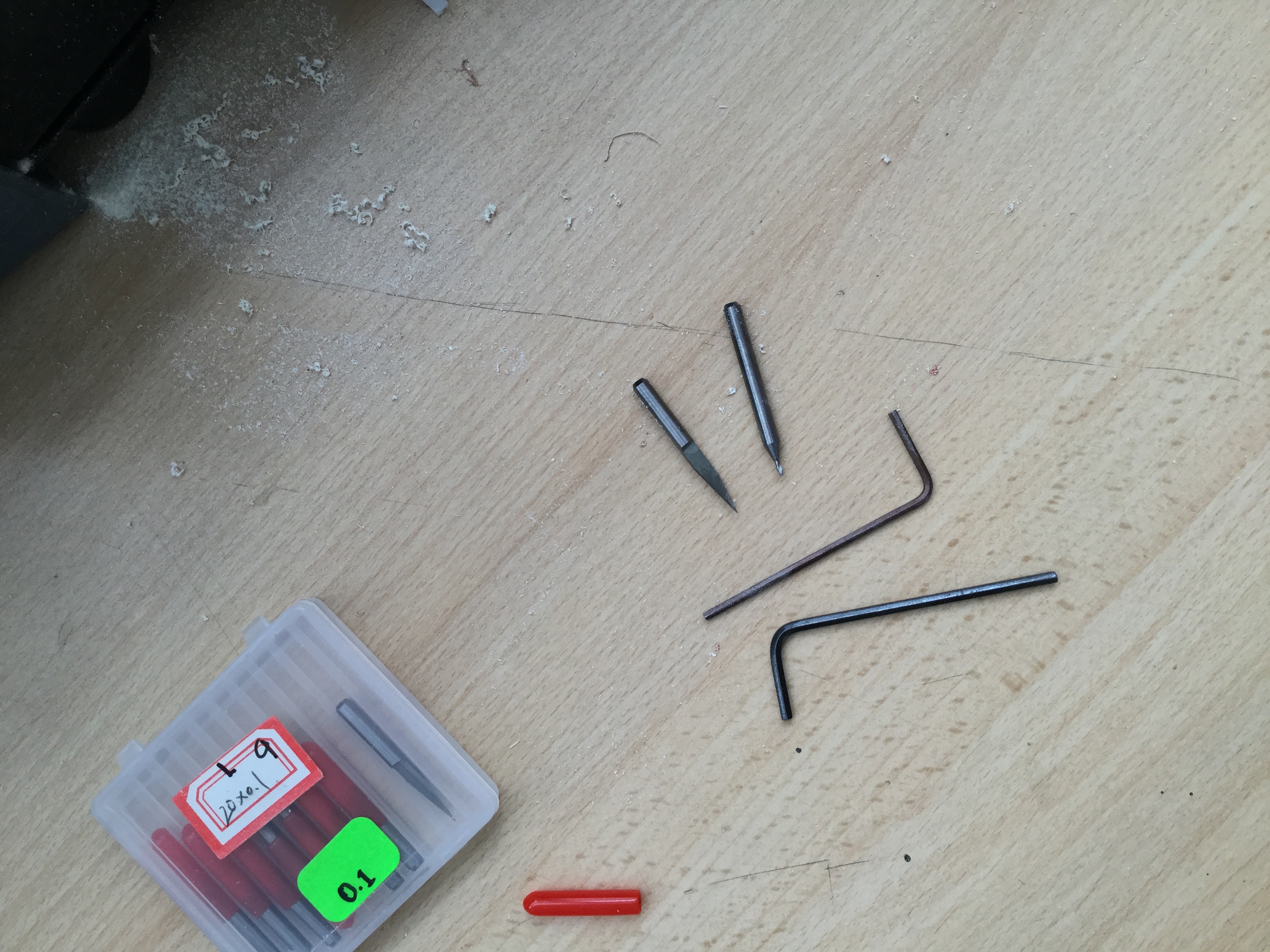
For me, the most critical part is set the milling machine, firt check if the mills are not break, then correctly secure the milling cutter to the machine head. To ensure the PCB on the machine a double-sided tape was used, this practice worked well when the board was small, but when we used a large board, a small inclination was generated causing an uneven cut.
.jpg)
Individual assignment
- Make an in-circuit programmer by milling the PCB, program it, then optionally, trying other processes.
Workflow
First download the mill and cut png files: traces and cutout
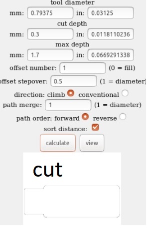
Then, i folow the same process of the gruop assignment, have carefull on the set of the machine and use the following parameter for milling and cutting:
.jpg)
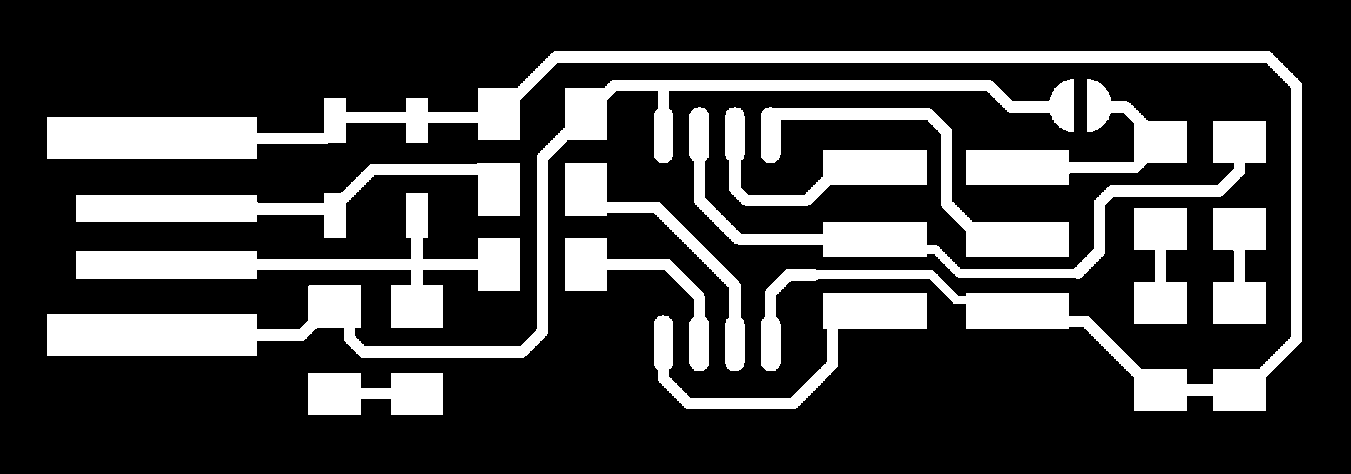
And have this result:
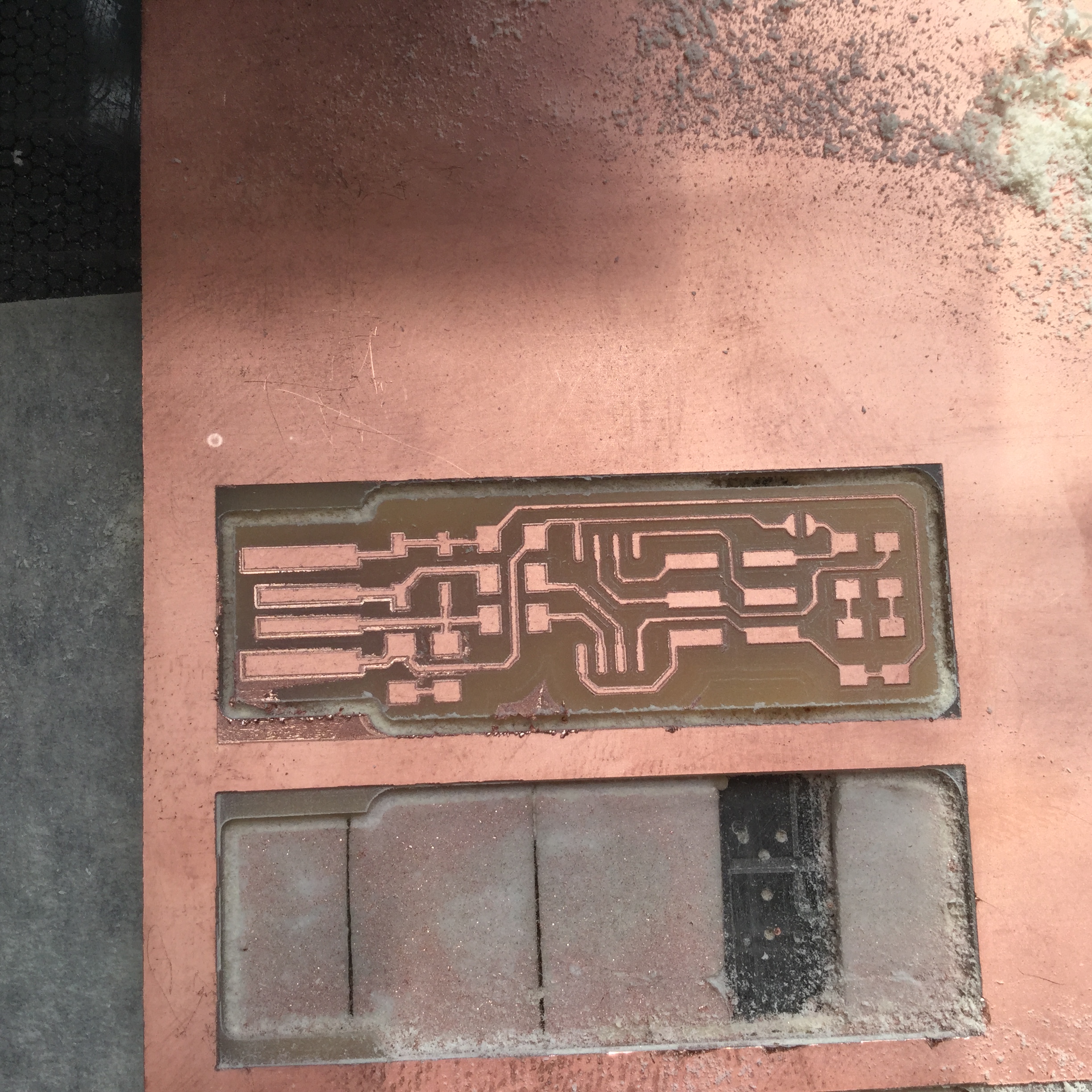
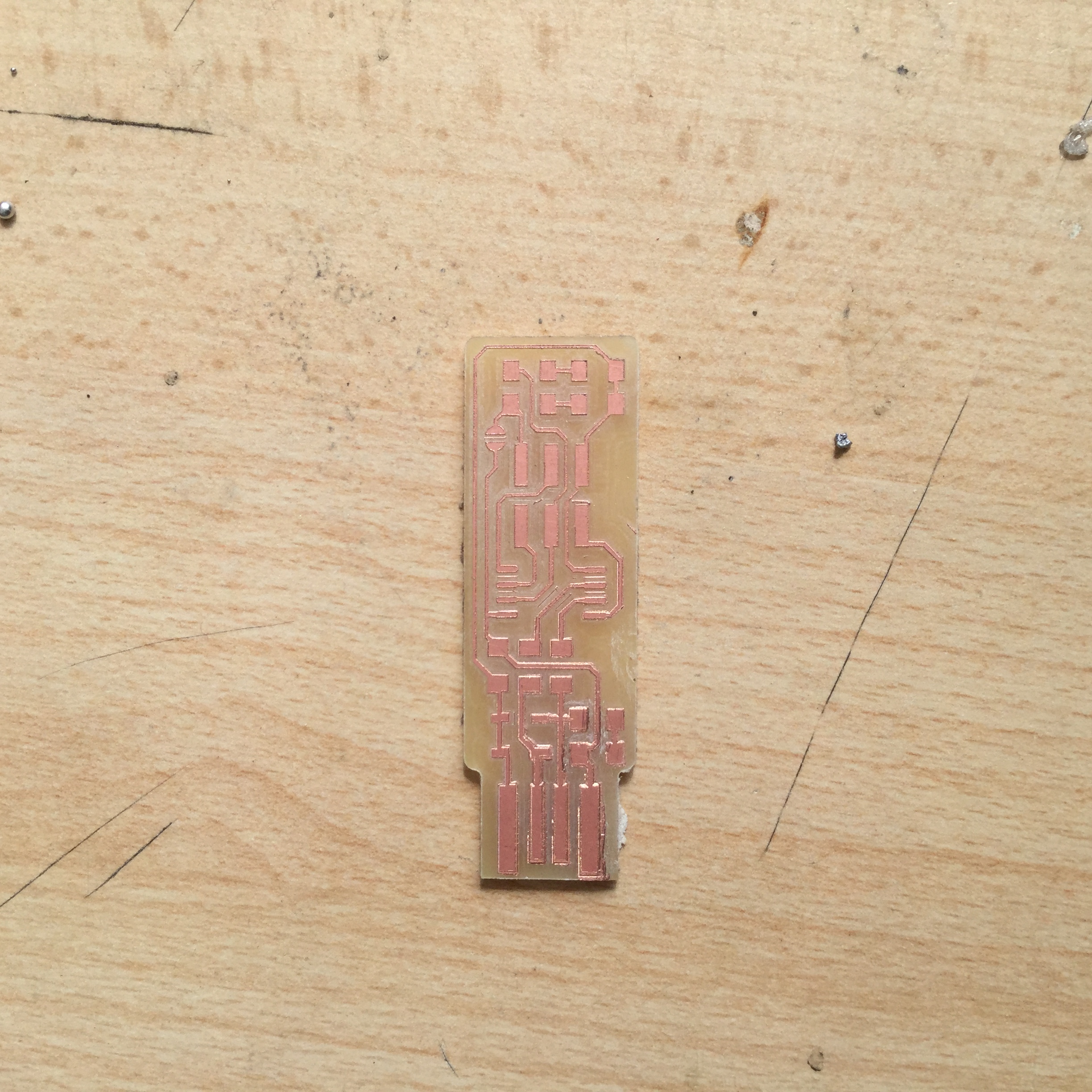
As see in the picture, the milling wasn't good enough, as a result of the inclination of the board due to the double side tape, so i have cut out a few the copper layer using a cutter. Finally the copper path seens good.
The next part consist in soldering the components en the PCB. The technique consists of melting tin using a resistance (soldering iron) and adding it to the copper. Before adding the tin we apply on the plate "flux" so that the tin better adheres to the copper. It takes a bit of practice because the components are very small and there is a risk of adding too much tin and this can cause paths to join the circuit and make a short
I use the Brian´s diagrams for assemble my PCB and use de following components:
- 1x ATtiny45 or ATtiny85
- 2x 1kΩ resistors
- 2x 499Ω resistors
- 2x 49Ω resistors
- 2x 3.3v zener diodes
- 1x red LED
- 1x green LED
- 1x 100nF capacitor
- 1x 2x3 pin header
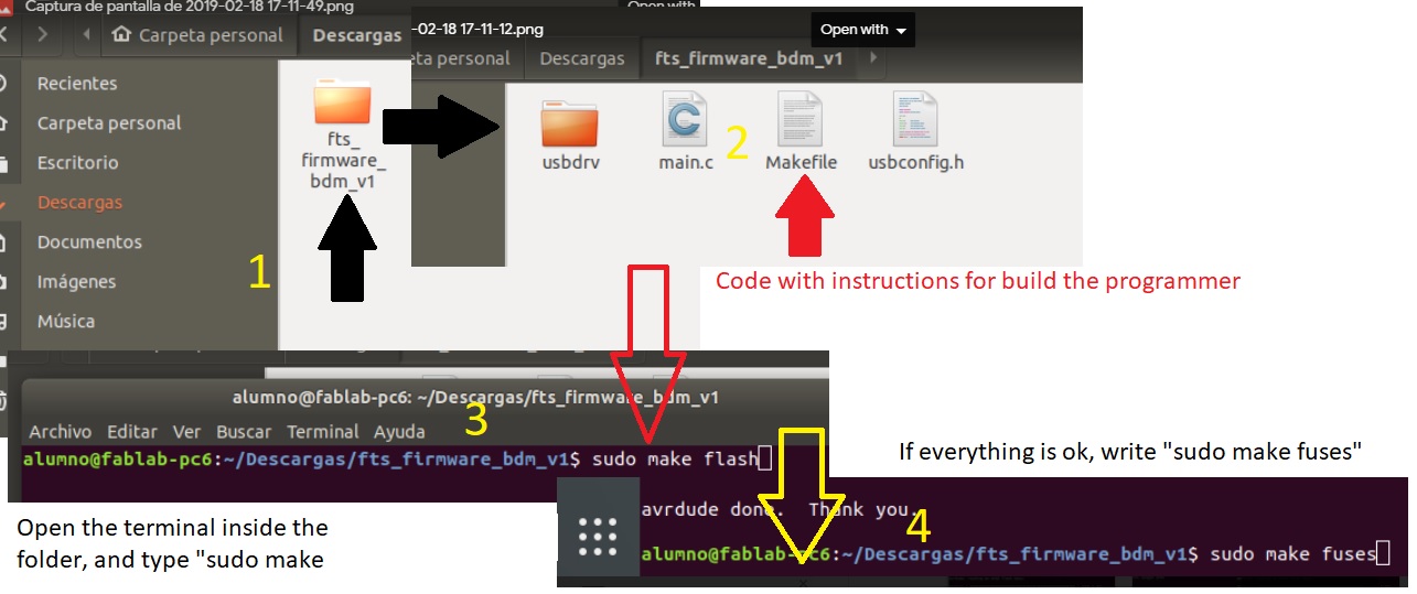
- In Linux/Ubuntu, download the firmware source code, then:
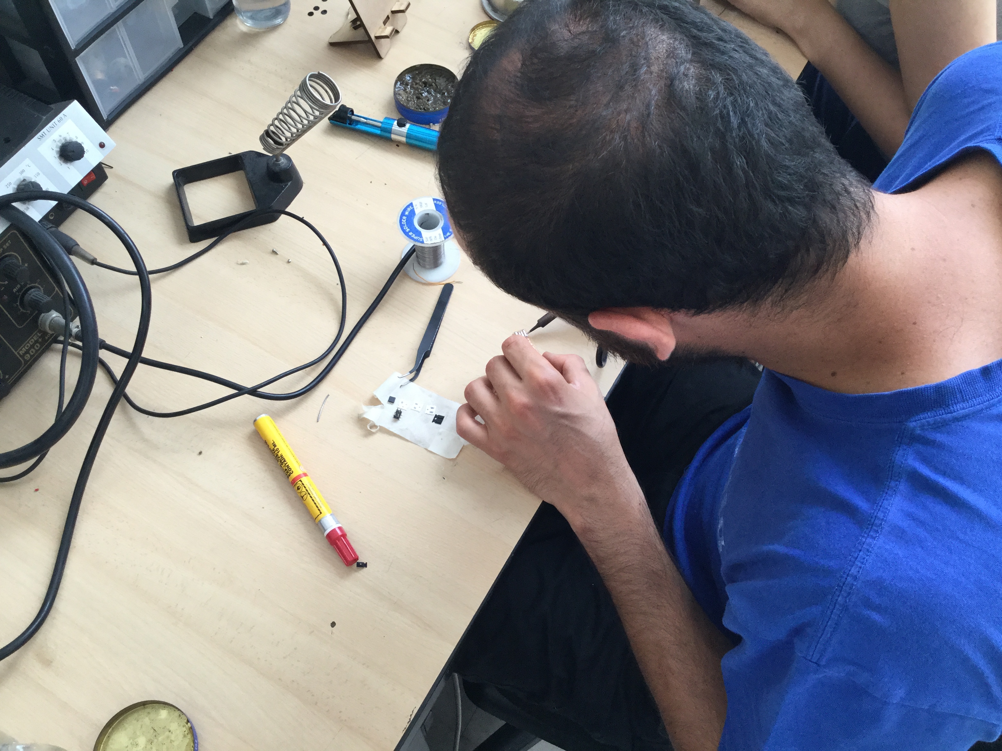
My classmates explained some important details to me, that some components, such as diodes or microchips can be soldered in a certain direction and for this they have small marks that must be respected, this can be contrasted with the diagram on Brian's page .
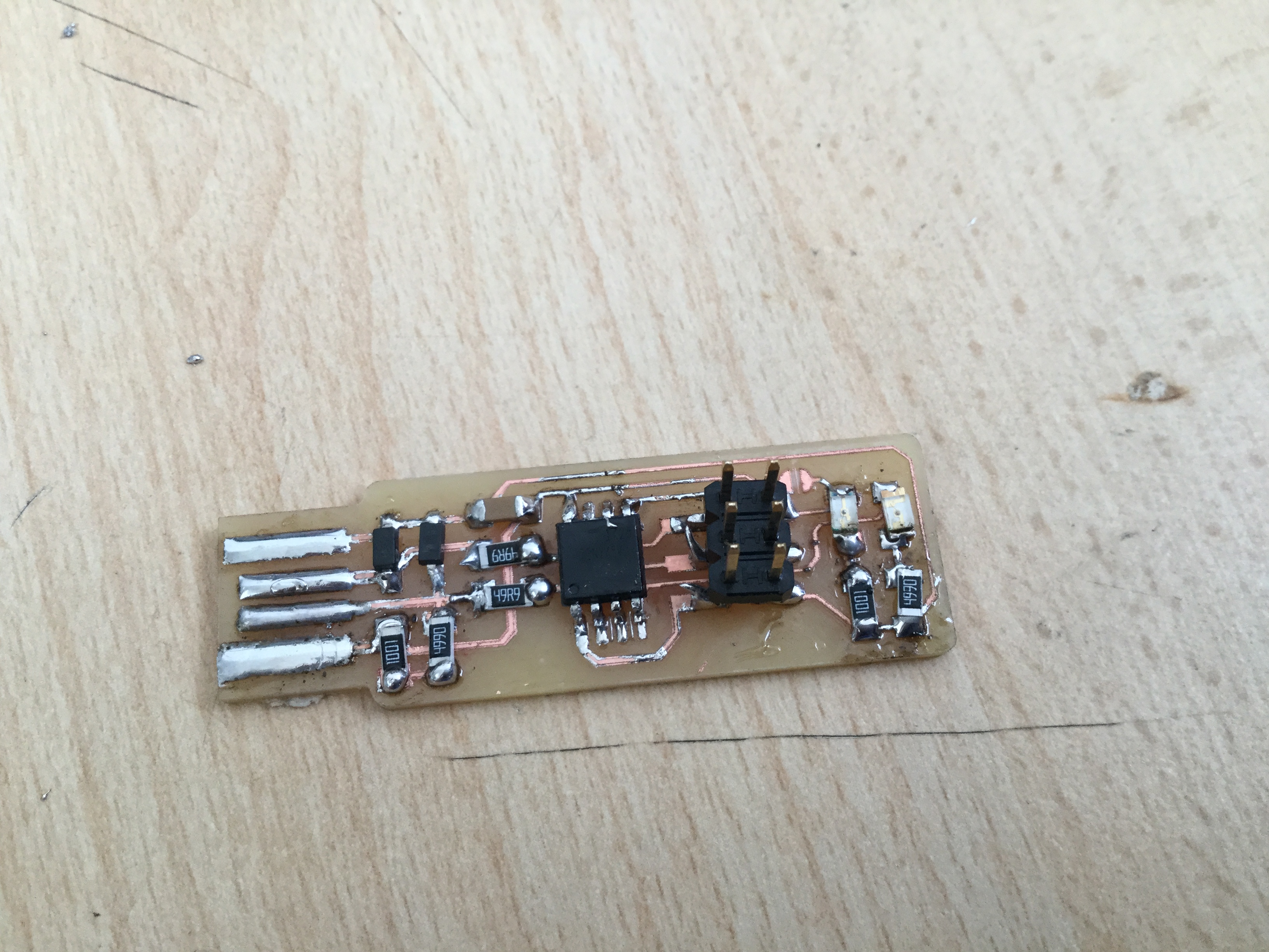
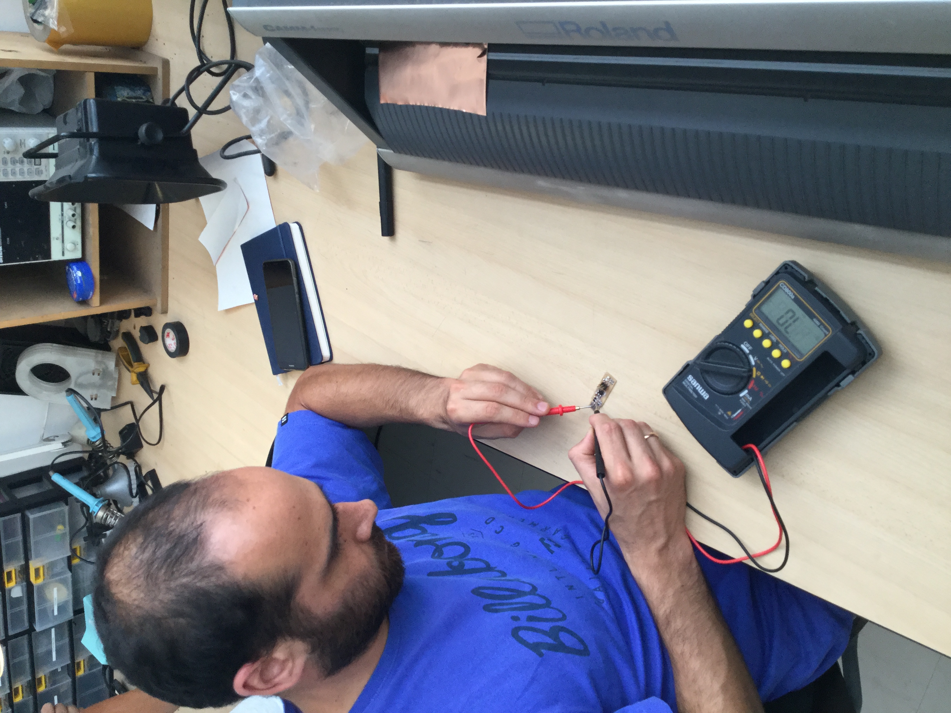
This was the final result. Then I used a multimeter to check if everything was properly soldered. I did this process twice, the first time I thought it was ok, but at the time of loading the program on PCB an error message came out, so I went back to check the circuit and found that I had two points that had not welded well , two pins of the ATtiny45 microchip, I had to add more tin and it was fine.
Programing
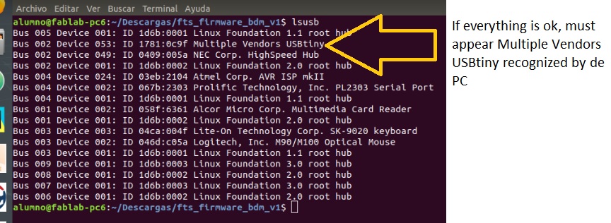
For programing, conect the PCB in a USB port of the computer, and at the same time conect the pin header to the ATMEL Small translucent blue programmer, if everything ins ok, the programer show two green lights
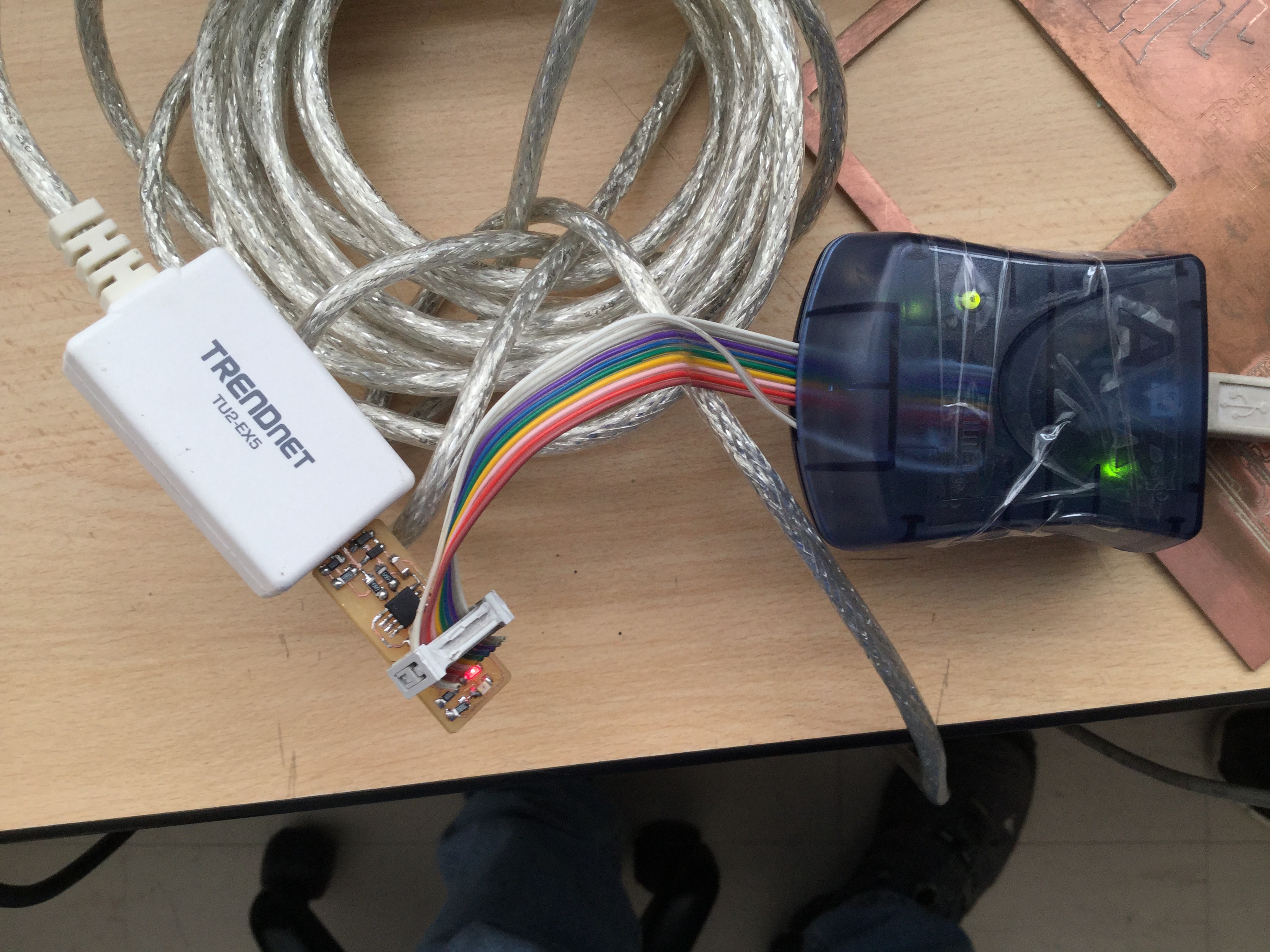
and finally to check that the program was recorded correctly

Learning outcomes
- Described the process of milling, stuffing, de-bugging and programming
- Demonstrate correct workflows and identify areas for improvement if required
Have you?
- Shown how you made and programmed the board
- Explained any problems and how you fixed them
- Included a ‘hero shot’ of your board