
Week 05
During the fifth week of the Fab Academy we were supposed to learn the basics of electronics production. It was a bit of a challenge, because the week overlapped with my participation in the FITC Amsterdam 2018 festival, where I ran a workshop and gave a talk about generative, data-driven and interactive projection mapping with the open source projection mapping tool that I am building: ofxPiMapper. Below you can see the opening titles of the festival made by Gavin Strange.
The assignment for the fifth week consisted of two parts: a group assignment and an individual one. The group assignment was about characterizing the specifications of one’s PCB production process. The individual assignment was to make in in-circuit programmer by milling a PCB and soldering SMD components on it.
PCB Production Process
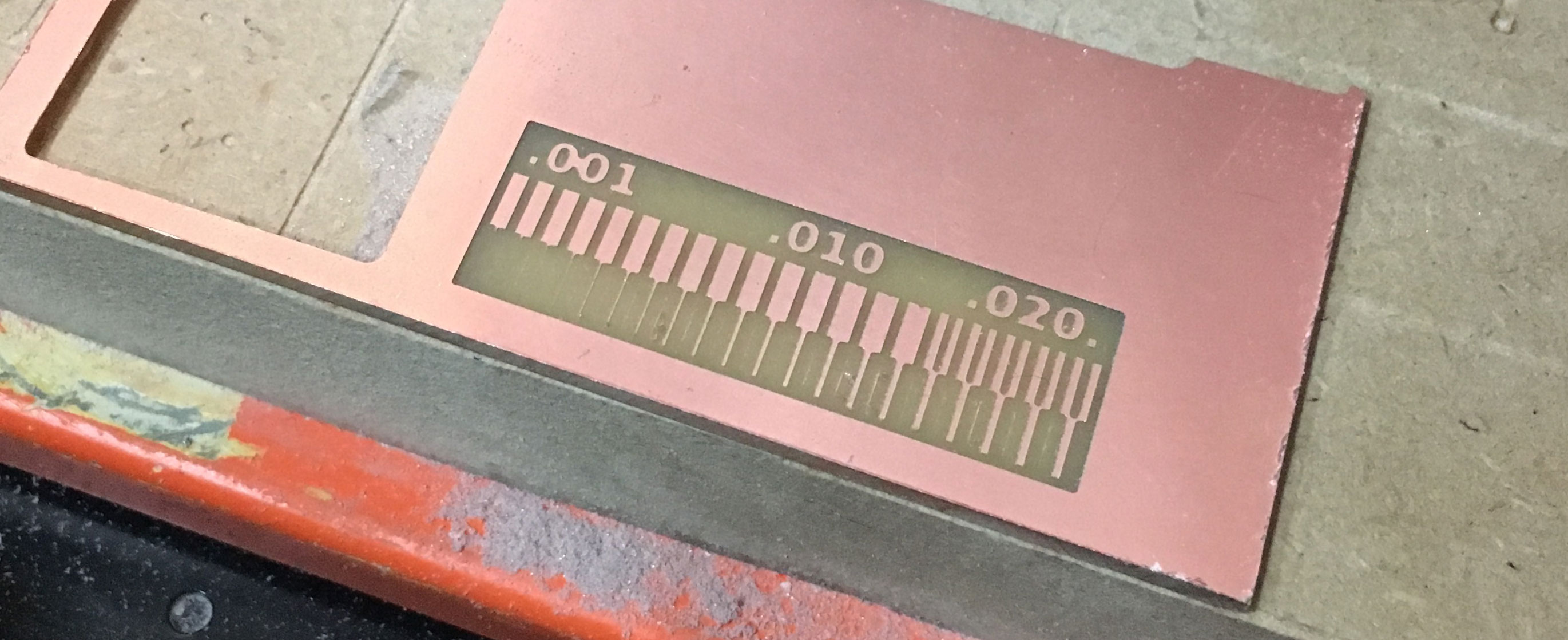
We teamed up with Dorota, Isaac and Ilias to explore the possibilities of the Roland monoFab SRM-20 milling machine. We went with the recommended test pattern design that can be found on the Week 05 (Electronics Production) assignment page.
Generating Toolpaths with Mods
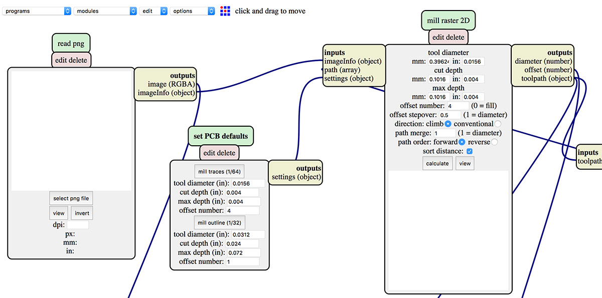
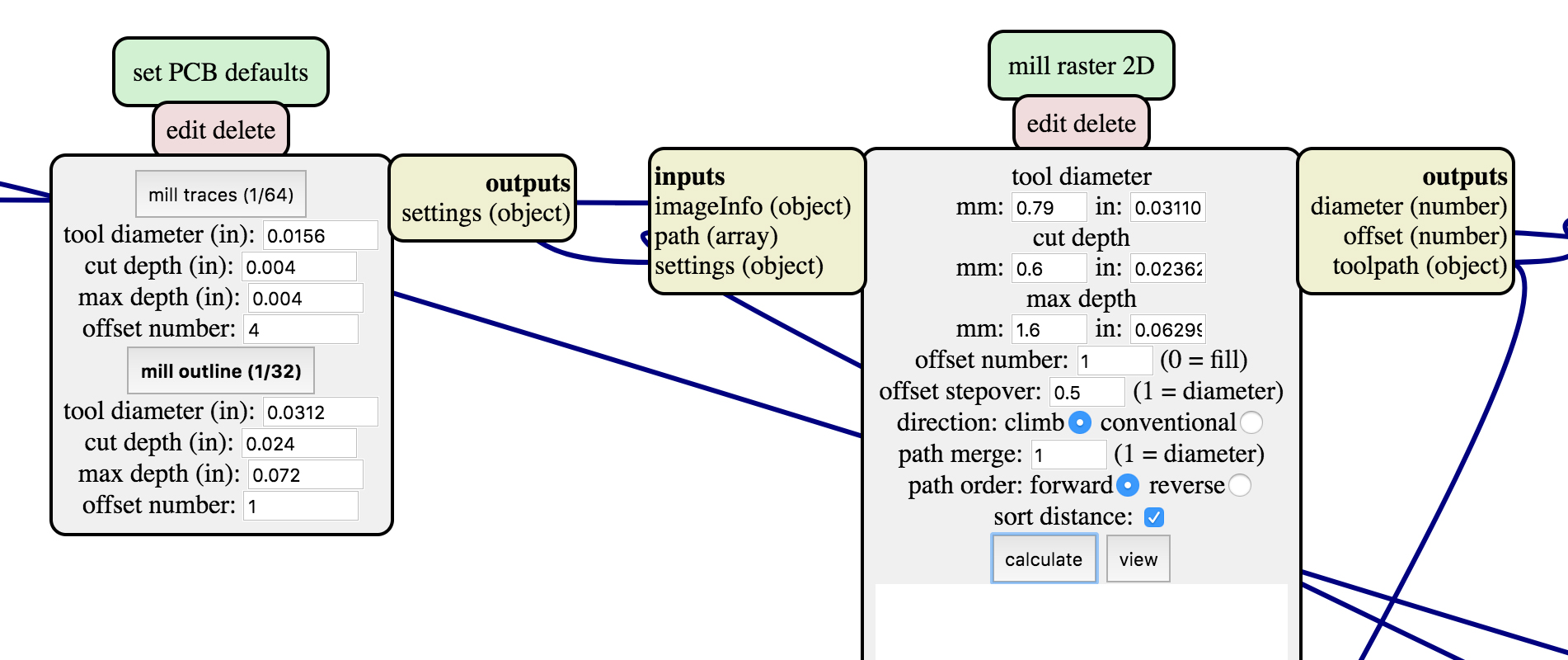
We used Mods to generate the toolpaths for the milling machine. When you open Mods in the Browser, first thing you need to do is to open a server program for PCB milling with the Roland SRM-20.
You should see a view of interconnected nodes (as in the image above) in the browser window at this point.
If you do not see a workspace consisting of interconnected modes, make sure that you have allowed the browser to open pop-ups.
First node in the workspace is the read png node where a .png input file has to be selected. Select the PCB milling test pattern called Traces file (you can download the image below) and proceed to the next step.

In the original Mods project file, the last node is the WebSocket device node. In our lab we prefer to use files. We replaced the WebSocket device with a save file node. The output from the Roland SRM-20 milling machine node has to be connected to the save file node.
The Set PCB defaults node contains milling defaults that we can reuse. There are two presets: for milling traces and for milling outlines. For our test pattern we went with the mill traces option.
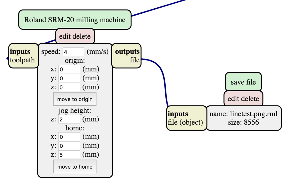
In the Roland SRM-20 milling machine node we set all the origin coordinates (x, y and z) to 0mm, set the jog height to 2mm and home position to 0, 0, 5 (x, y and z respecitively).
The mill raster 2D node has to be edited in order to match the tool properties. Since we use a 1/64in tool for milling traces, we specify the tool diameter as 0.4mm, which is a rounded value of 1/64in. For the cut depth we have to specify how deep the tool will cut in one pass. In the case of cutting traces, 0.1mm is deep enough. We are not going to cut any deeper this time, therefore set the max depth to the same value.
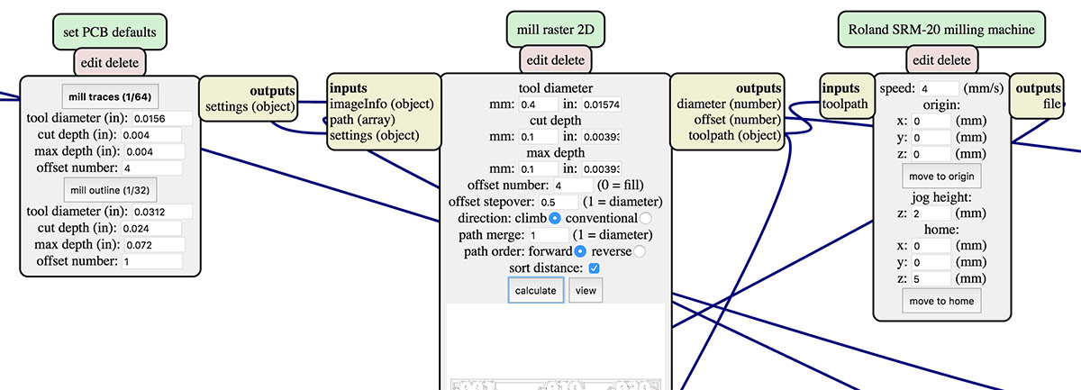
Then one has to hit the calculate button to calculate the toolpaths for the mill. Once Mods has done it, the browser will offer you to save the .rml file. Mods will also open a toolpath viewer for doing a visual check-up of your paths.
Setting up the Machine
First thing one has to do is to position the material on the base plate od of the machine. We used double-sided tape to make the FR4 copper clad to stick to the base plate of the SRM-20. It is possible to remove the build plate from the SRM-20 by releasing the four bolts near the corners.
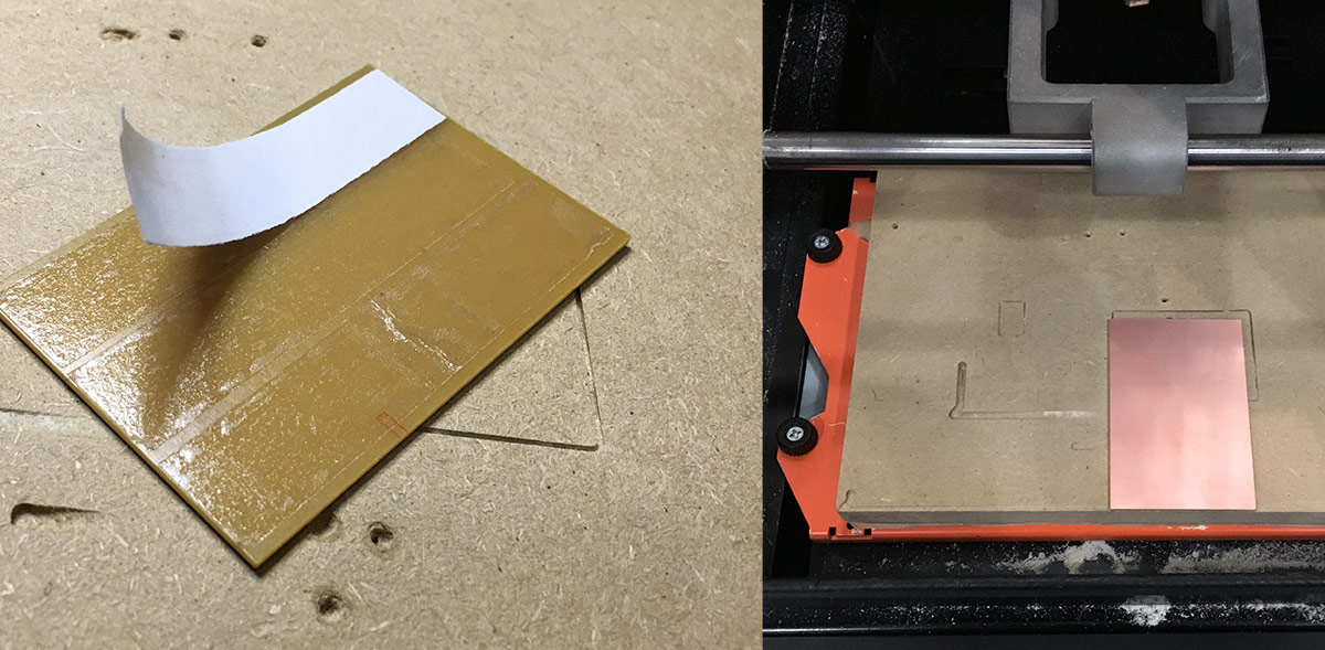
Then we installed the 1/64in (0.4mm) milling tool and turned on the machine. On the connected PC the Roland VPanel for SRM-20 software had to be opened.
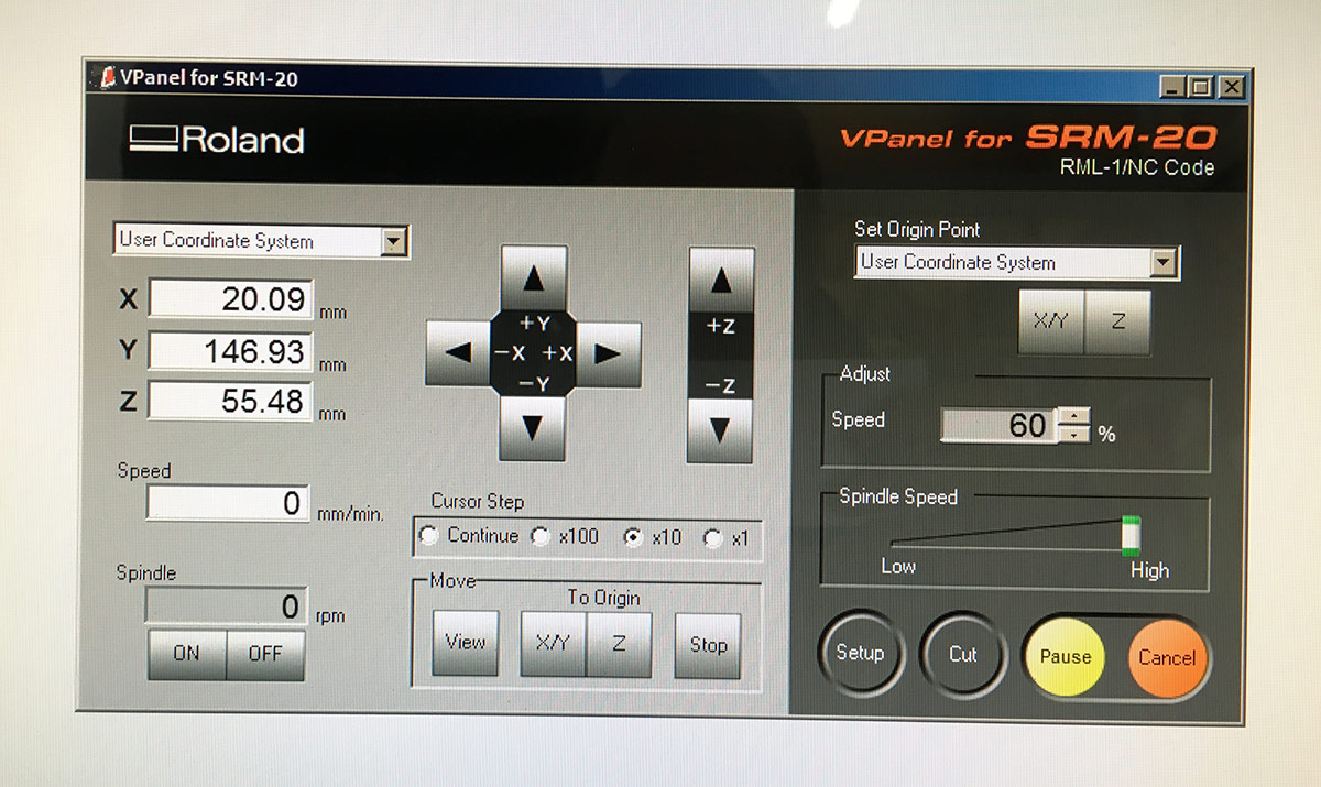
Home positions have to be set for x, y and z axes before loading the toolpath file for milling. Rough positioning above the material is possible by selecting the Continue Cursor Step and then using the +X, -X, +Y and -Y arrow buttons. When the tool is above the material to be milled, use the x10 Cursor Step to move the tool closer to the surface of the milling material.
Release the bolt holding the milling tool in place, so it drops and touches the copper surface. Fasten the bolt, but don’t be too hard, since the thread is fragile. Once that is done, the Z button has to be hit in the Set Origin Point section on the right side of the VPanel interface.
Carefuly use the +Z arrow button to lift the tool a few millimeters above the milling surface. Then use the X and Y arrow buttons to position the tool on the bottom left corner of your material. Hit the X/Y button in the Set Origin Point section in order to set the x and y home position.
Set the speed value to 10% initially, you will be able to go up to 60% during the actual milling process.
It is safer to start slow and act accordingly when you see a milling job failing slowly than feel sorry after it happened too fast for you to notice.
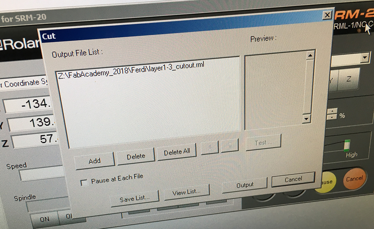
Hit the Cut button to load the job. Remove any previous jobs before adding a new one. Click on Output button to send the job to the machine. Observe. If everythings seems well and you can see that the mill is moving along the path you recognise, you can gradually increase the speed up to 60%.
The following image shows the result of our first milling pass.
Another milling pass has to be done in order to cut the board out of the copper-covered FR4 board. In order to do that we have to go back to Mods and select a different PNG file from the Week 05 assignment page, called Interior (the link loads the same image displayed below).

A few adjustments have to be made in the set PCB defaults node: one has to hit the mill outline (1⁄32) button to load tool parameters for the 0.8mm diameter tool. Then one has to hit the calculate button in the mill raster 2D node to recalculate the toolpaths. We leave all the origin and home-related variables in the Roland SRM-20 milling machine node the same as for the tracing step.
For the Roland milling machine, one has to change the tool. This time it is going to be the 1/32in or roughly 0.8mm diameter tool. Recalibrate the Z axis after changing the tool. Leave the X/Y origin the same as for the tracing step.
Make sure the Speed is adjusted to 10% before you continue.
Hit the Cut button to open the job loading interface, clear all the previous jobs by clicking the Delete All button. Load the .rml file that you generated for the cutting step of the test pattern and hit Output to send the job to the machine.
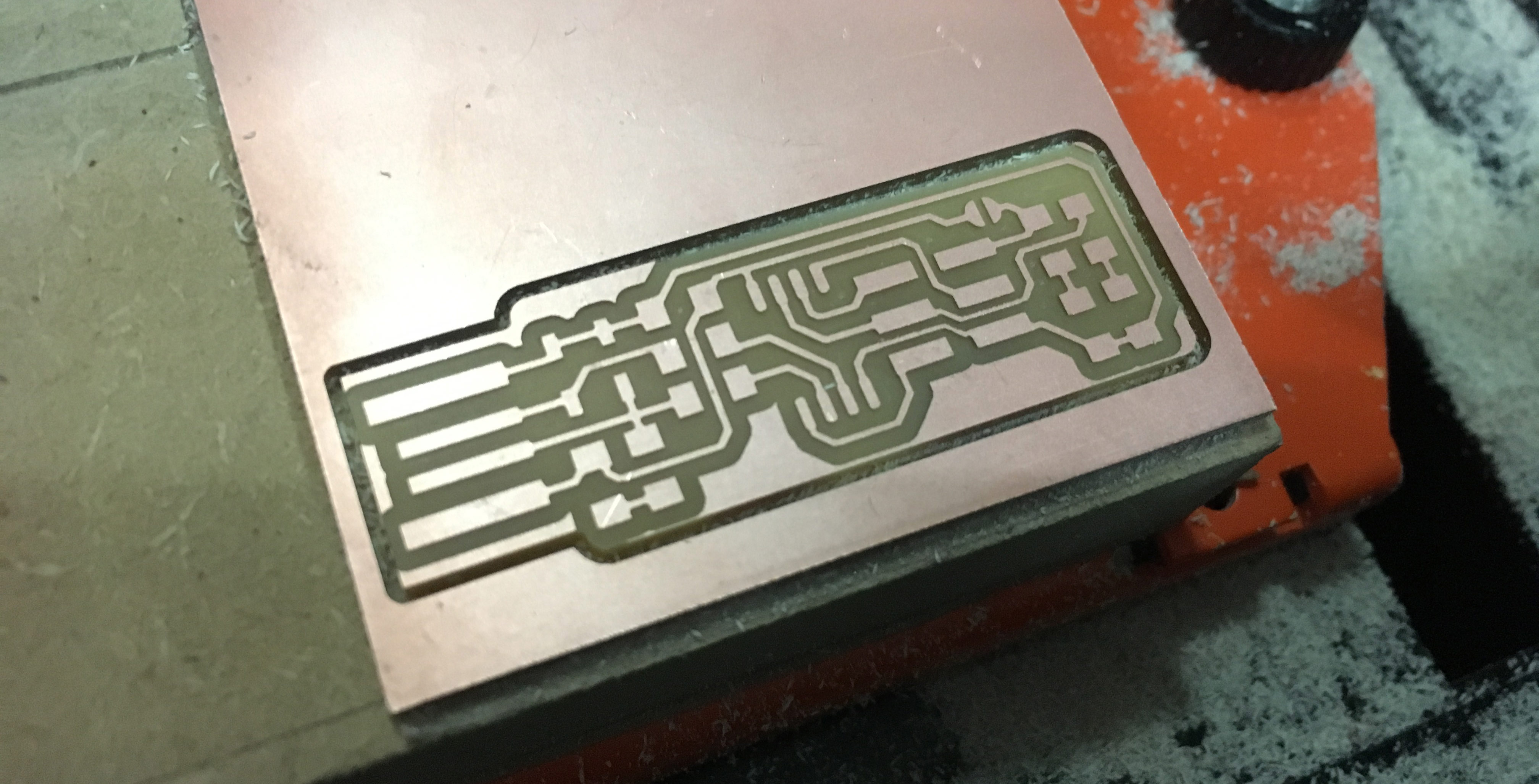
Watch the process carefully and if you see that the tool is moving along the paths that you expect, you can increase the Speed adjustment up to 60%. In our case everything went fine and you can see the finished test PCB in the image below.
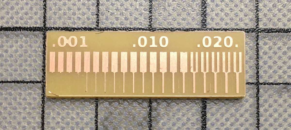
As you can see, the thin lines on the left side were not cut. My guess is that it could be because the tool diameter setting was not hight enough. Instead of 0.79mm we should have used 0.8mm. Below you can see a video that shows dust removal and how to take the ready part out of the machine.
All of us were sattisfied with the final result and we went on to do our individual assignments.
Making an In-Circuit Programmer
For making my In-Circuit programmer I chose the FabTinyISP instructions by Brian from the Fab Academy Assignment description page. For the milling I went with the process described above, using Mods; traces and outlines from Brian’s tutorial page.
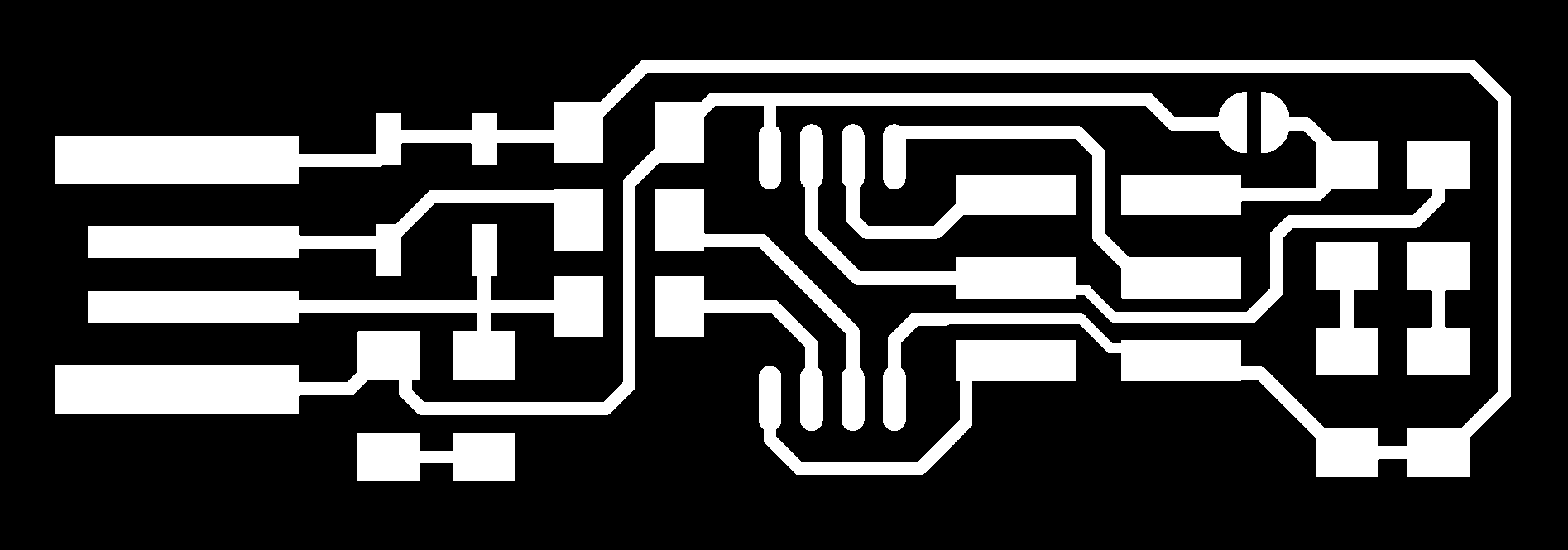

Looking at the material provided, I tried to understand, how should I position my design in order to be able to make as many boards as possible. The FR4 copper coated board provided was 75x50mm. I could not find the dimensions of the final FabTinyISP board, I found out that Mods has a view toolpath node where one can see the final dimensions of your cut.
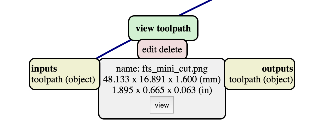
From here one can tell that the dimensions of the material needed are 48.133x16.891mm which makes it possible to position our material perpendicularly against the design and rough calculation tells us that we can make 4 PCB’s if things go well.
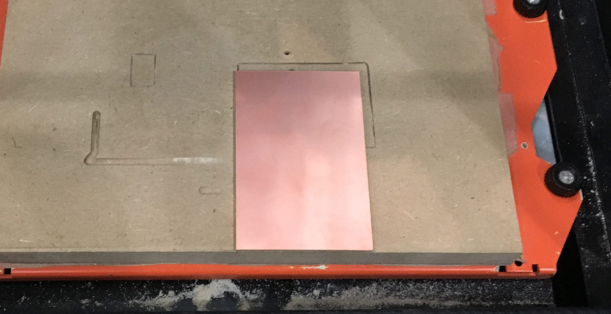
Position the board using double-sided tape.
Make sure that it adheres very well.
If you do not, the board will start to jump during the milling process and your job will fail. You can see a lucky result in the image below. At this point I was able to cut the board out by using a sharp knife.
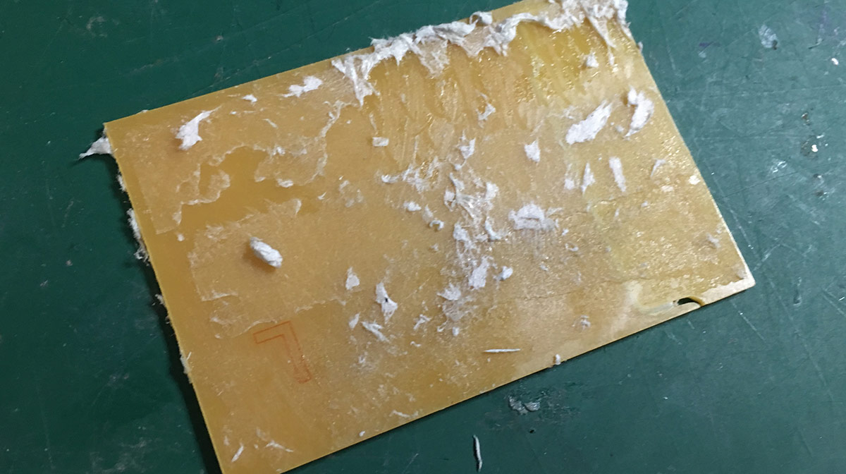
Another thing to note is the following.
Remove all leftovers of tape before proceeding with alcohol and paper towels.
Otherwise you will end up with a sticky and ugly mess like I did.
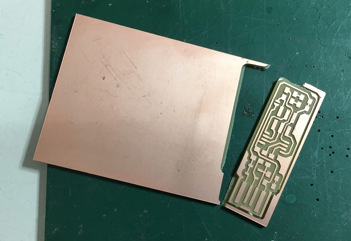
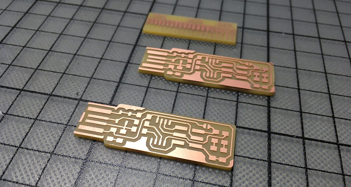
After solving the two problems mentioned above, I ended up with having a perfect trace and cut, as you can see in the image below.
At this point I had two PCB’s, just in case the soldering does not go so well with the first one.
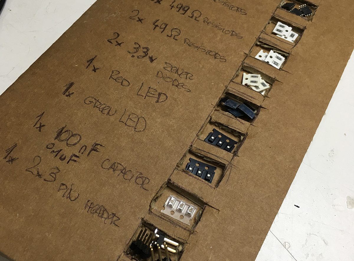
Next step was looking for the parts mentioned on the instruction page. Since the SMD parts are very small and it is hard to tell what component a tiny SMD particle is, I decided to make a simple cardboard SMD project plate with labels and pockets for each of them.
I also managed to get a reference board with components already soldered on them. That made it much easier to understand how to accomplish the rather detailed work of soldering.
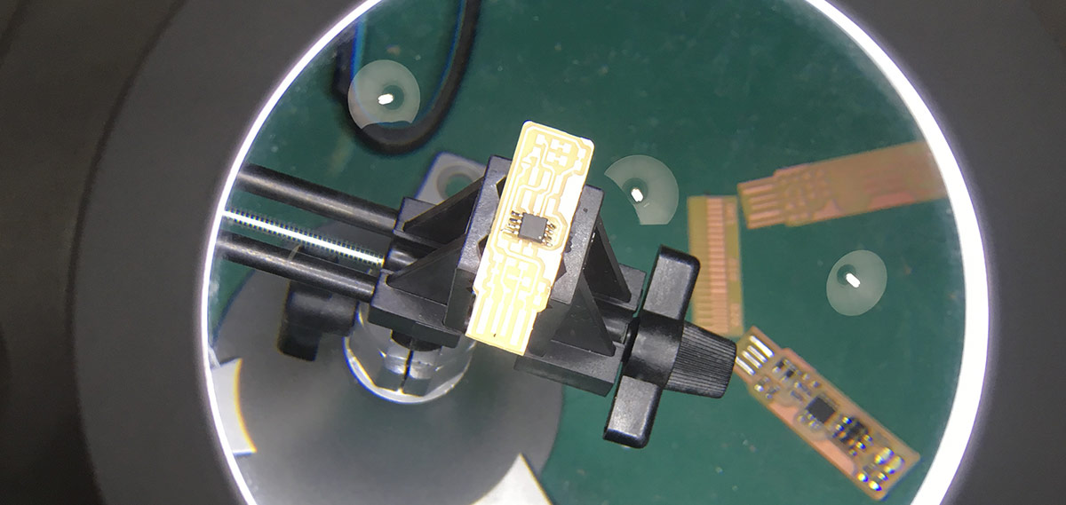
I used a LED light equipped loupe to have a better view of the details of the board. That helped a lot and from my previous experience with soldering, I always felt I need more light, which was not the case here.
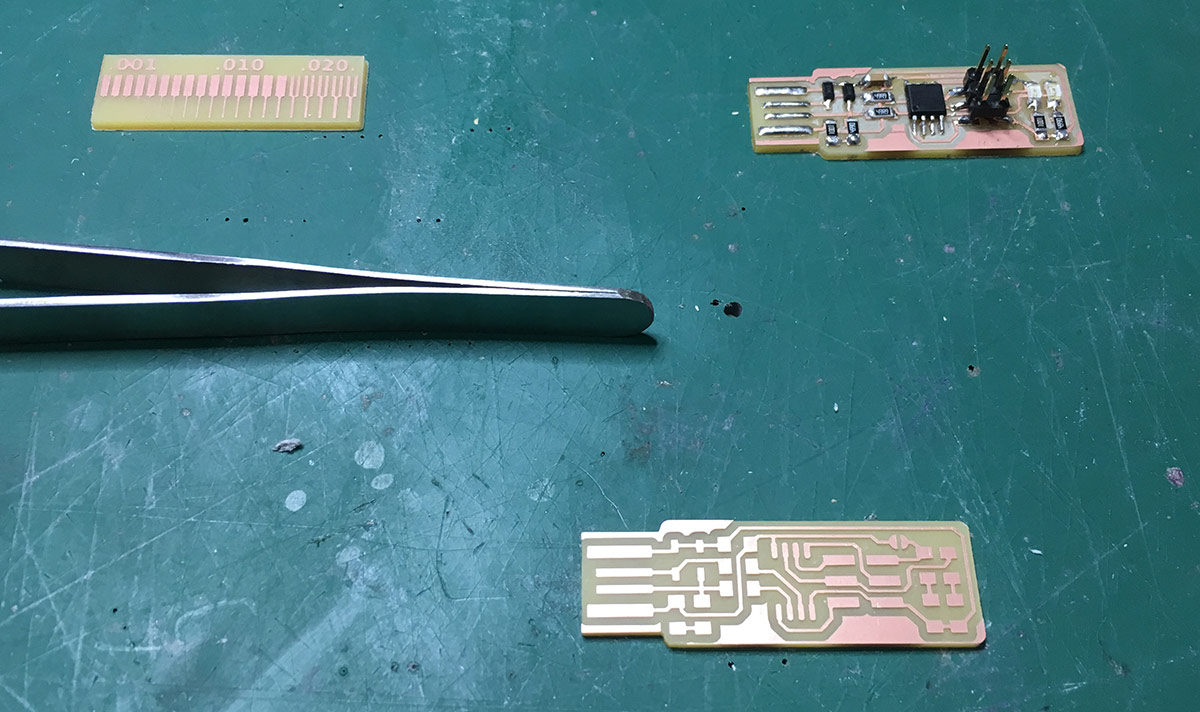
After listening to the Fab Academy video instruction on soldering and watching SMD soldering videos on YouTube I managed to gather enough courage to begin doing it myself. It took a bit less than 2 hours with a break in-between. Below you can see the final result.
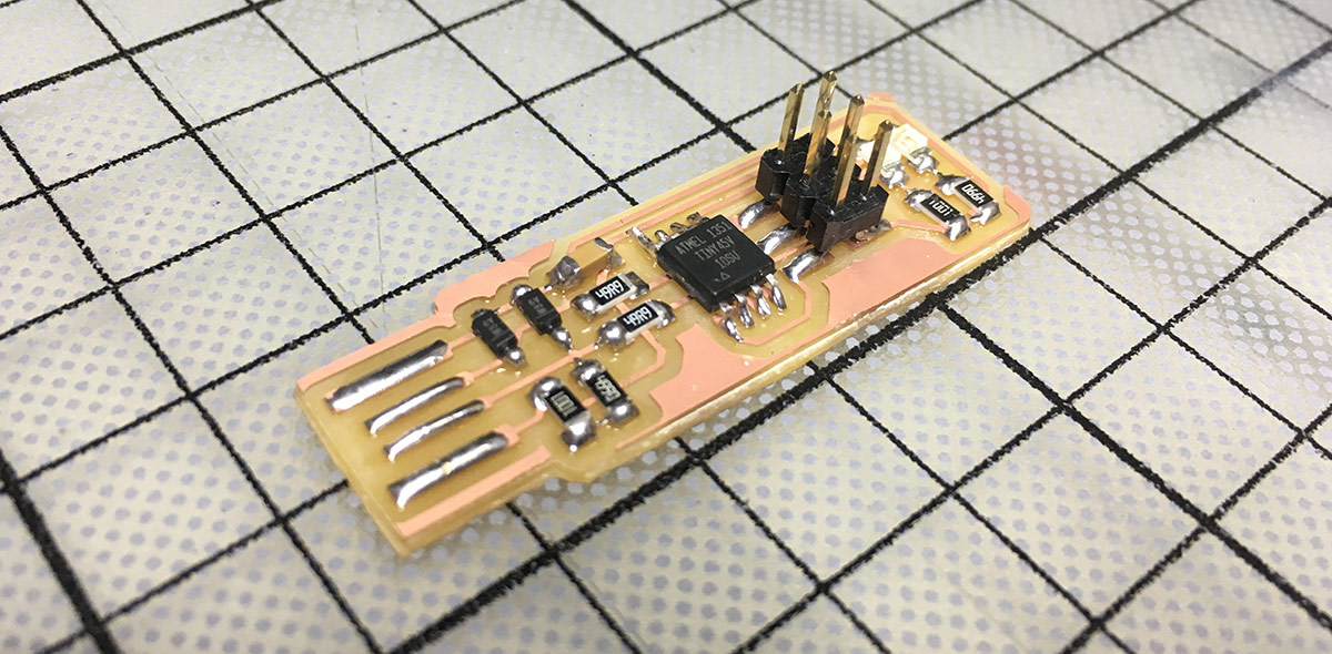
Since SMD soldering and production of my own circuits is one of my main motivations in this course, I decided to go the full way and attempted to program the board. I took one of the available AVRISP2 programmers available at the Fab Lab Barcelona.
Prior to connecting cables, I downloaded CrossPack AVR developmment pack for Mac OS. The installation script puts all the needed programs under /usr/local/CrossPack-AVR/bin, I had to add this to my PATH in order for things to work.
After downloading the source code unzip it in a safe place and navigate to it by using Terminal and the cd (change directory) command. Then type the following.
make
Hit enter, it should output this.
AVR Memory Usage
----------------
Device: attiny45

Program:    2488 bytes (60.7% Full)
(.text + .data + .bootloader)

Data:         75 bytes (29.3% Full)
(.data + .bss + .noinit)

avr-objcopy -j .text -j .data -O ihex fts_firmware.elf fts_firmware.hex
This means we have successfully compiled the source code and have our firmware (fts_firmware.hex) ready to be flashed to our board.
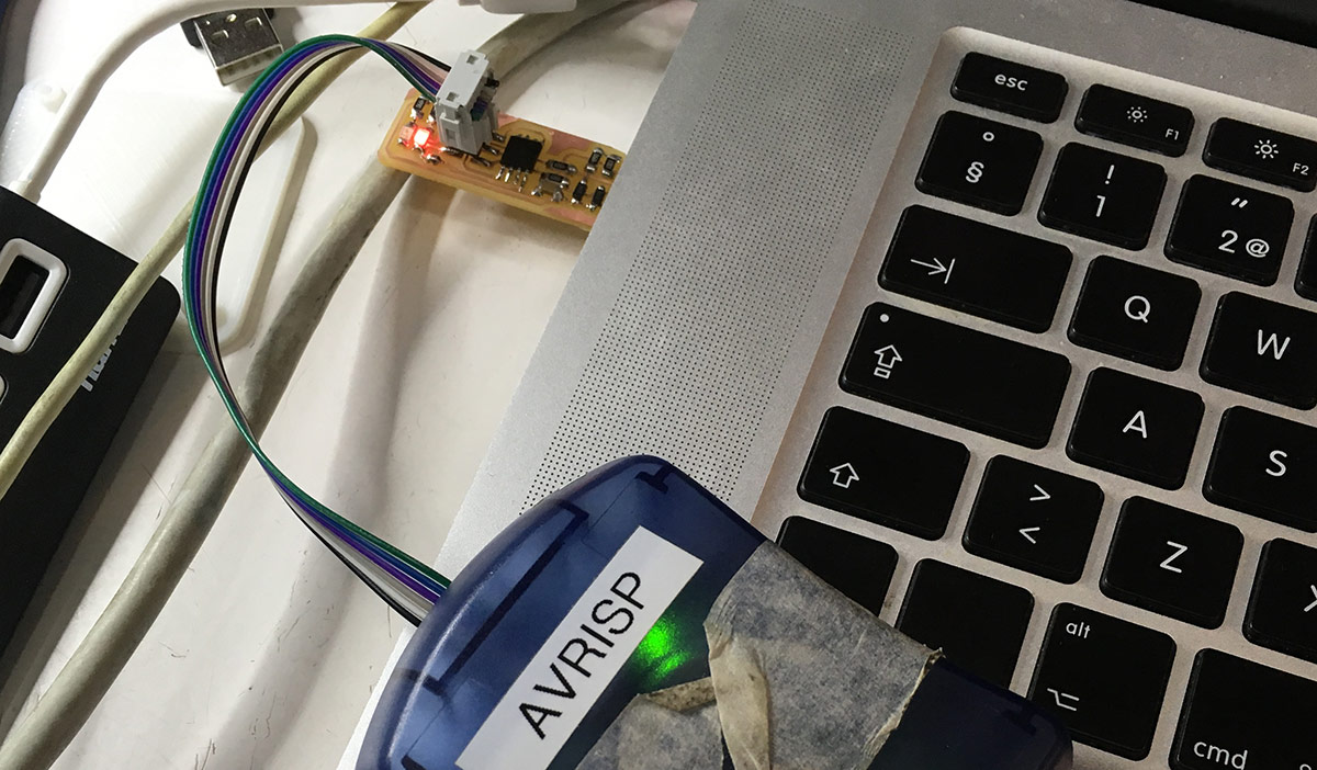
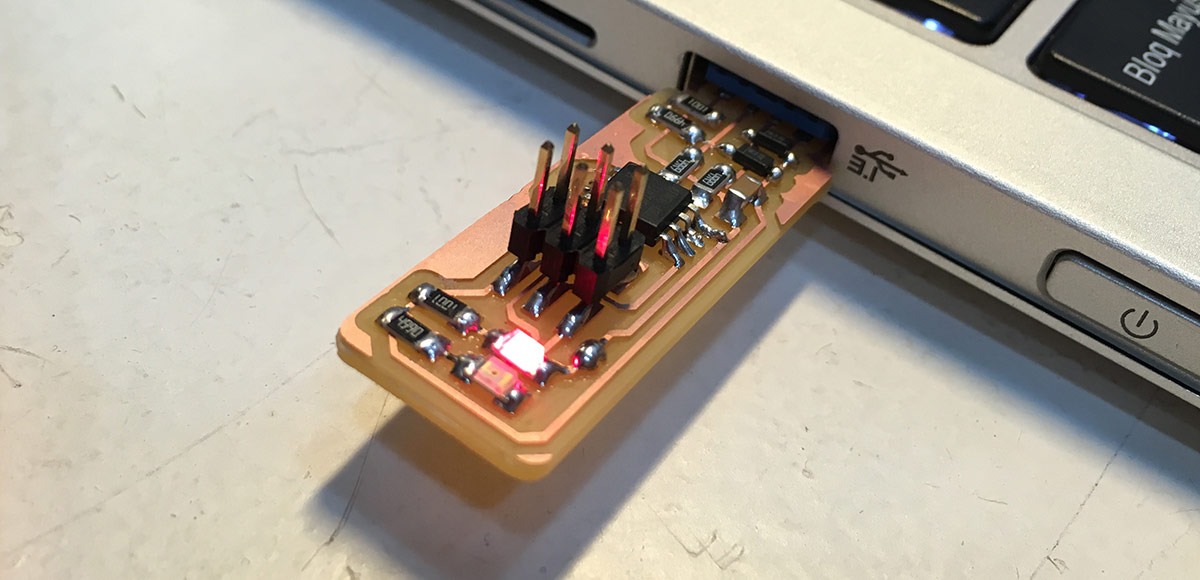
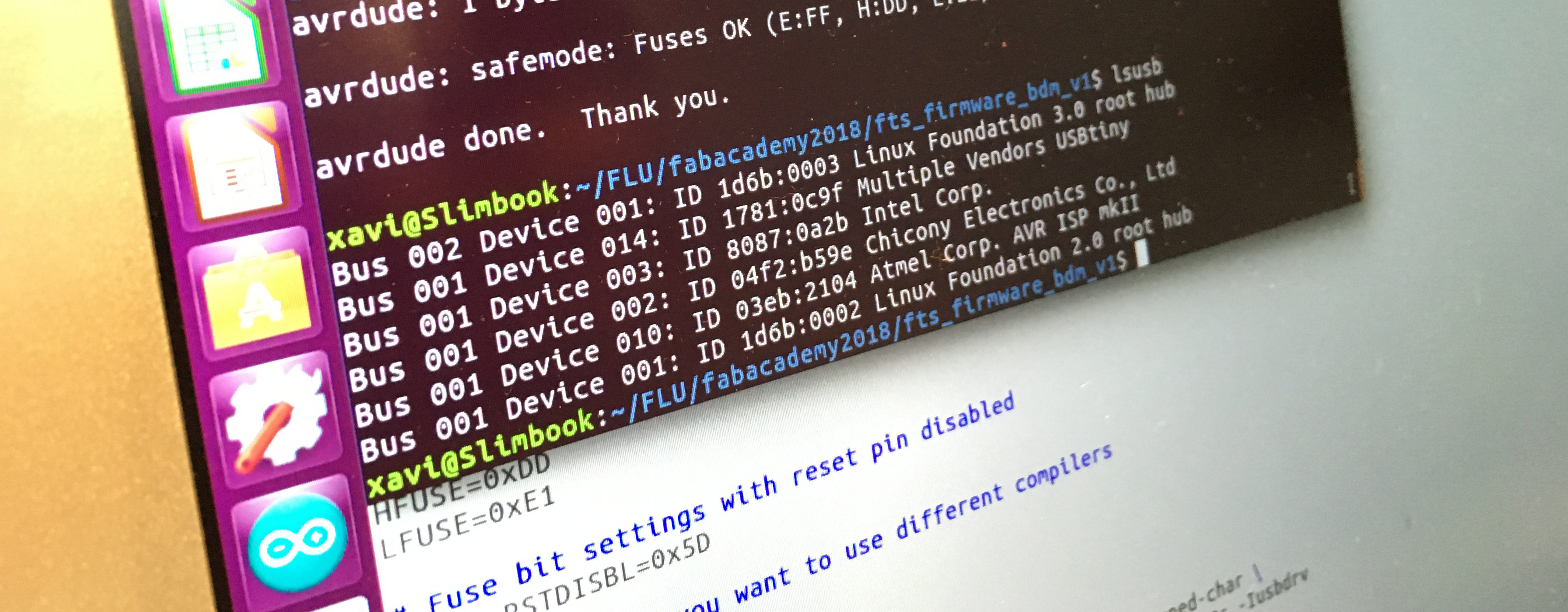
I plugged the programmer’s USB cable in one of my computer’s USB port. Since I could not find an USB extension for my FabTinyIsp board, I went for the risk and plugged it in directly. And it worked (the light on the programmer turned green, which means the communication with the target board works just fine).
After programming the board I failed to detect it on my Mac computer. I tried it on Dorota’s Mac and it did not show up there neither. Xavi helped me with his Ubuntu machine and we were able to see it there by using lsusb terminal commmand. Later I tried to connect the board to a Windows machine and it showed up there as well.
There are more things that one could do at this point.
- Try to find out what is wrong with Mac’s.
- Try to program another FabTinyIsp by using my brand new programmer.
- Make another one.
Making LeoISP with KiCad
Unfortunately it was not possible to get the FabTinyISP of Brian working. I made two copies, was able to programm it, but it was not possible to use it for programming other boards. Therefore I was not the only one who faced this problem. Below are some things that I tried to do in order to make the FabTinyISP working.
- Compile CrossPack from source.
- Program FabTinyISP from a Linux machine.
- Make another FabTinyISP and follow the steps once more.
No success. Nevertheless there were some students in the class that claimed that their version works. After gathering the details, I noticed that they were using the ATtiny44 version of the ISP programmer. I decided to make it as well.
This time I thought it is a good idea to use KiCad. I heard somewhere that it is being used in CERN and therefore is cool. It is also open source and free, which makes it even more reliable. Below is a YouTube tutorial which gives a nice overview on what is possible with KiCad.
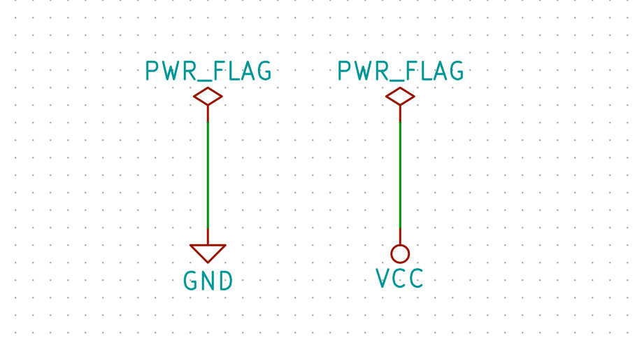
I started to design my schematic and it went well until a weird error during the electrical rules check appeared.
Pin connected to some other pins but no pin to drive it
What one has to do is to add PWR_FLAG to GND and VCC of the circuit. KiCad has to know that the power is coming from somewhere and if it is not a battery, PWR_FLAG has to be added. Add the following to your schematic somewhere. Use the P key to look for the right symbol.
Sorry, got no time to continue on this one.
Conclusions
It was a fun week! Electronics was the main thing I was looking to improve at during the Fab Academy course. I have never used SMD components in my designs. Always started with a breadboard, a maze of jumper wires and only through-hole components.
I learned a lot in terms of milling, looking for components and soldering. What I was dissapointed with was that I could not get the programmer working event after making it multiple times (I was not the only one who had problem with the programmer version of Brian).
Apparently fellow students who used the ATTiny44 version of the ISP programmer got a working programmer at the end of the week. Not me and not the ones who were using the ATTiny85 version by Brian. This is why I started to document a fresh attempt of making an ATTiny44 version with KiCad. I will have to finish it after the course though.