Electronics Design
This weeks assignment was to redraw the hello world board and add a button and LED to the PCB. Eagle was the suggested tool of choice however I would much rather use and open source EDA tool so I decided to give KiCad a go.
Schematic capture in KiCad is pretty straight forward. However there are graphical glitches when you move things and ghosted versions are left behind. Forcing a redraw by zooming fixes it though. Probably the most annoying aspect is moving elements since it will just disconect components and now try and intelligently reroute the connecing wire. Using the keyboard shortcuts are a must to be able to do anything in a reasonable amount of time. There are good tutorials available for KiCad by Chris Gammell https://contextualelectronics.com/course/kicad-tutorial/.
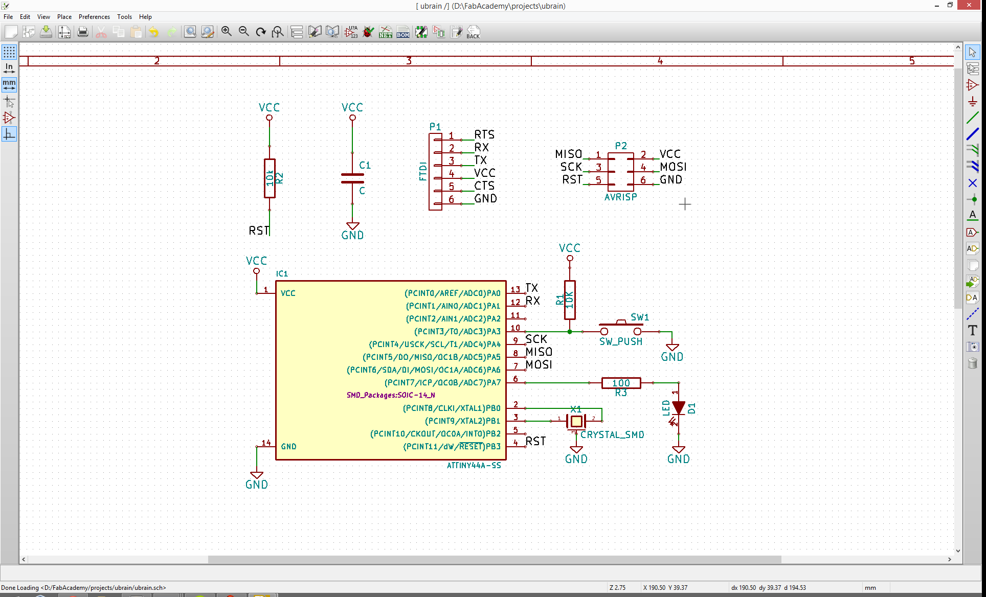
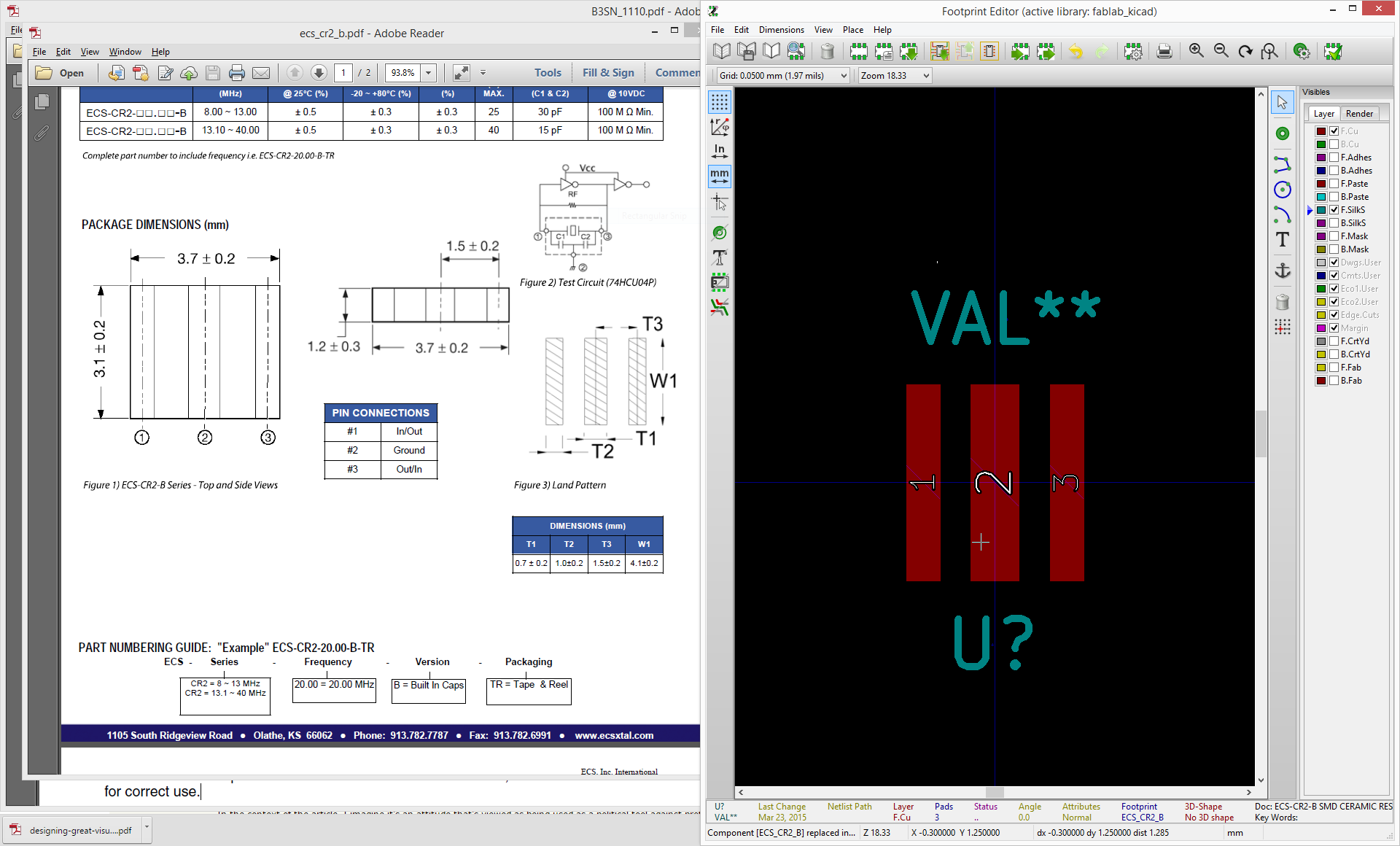
The first stumbling block was the lack of footprints for some of the components needed for the board like the 20MHz resonator and SMD 2x6 headers. After finding the datasheets to get the recommened pad layout, using the footprint editor to create the footprint was straighforward. However I had the set the active library in both the schematic editor and pcb layout tools to get it to make the footprint available.
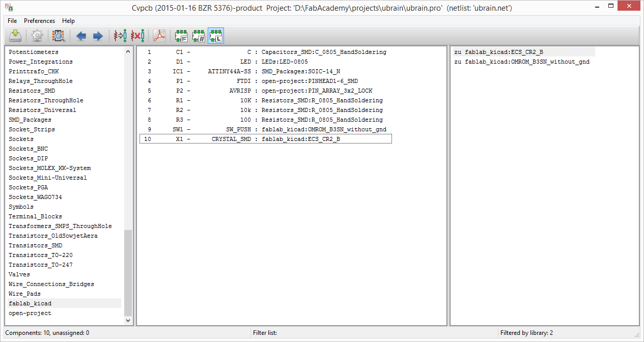
KiCad has an interesting workflow where you use another tool Cvpcb to assign components to the footprint. When you are ready to start laying out the board in the schematic editor you generate a netlist, use Cvpcb to select footprints then jump into the pcb editor and read in the generated netlist. It makes round tripping changes a little awkward, but is bareable.
PCB layout wasn't too bad selecting compoents tearing up traces and moving components was a bit annoying because of ghosting and having to get the cursor in just the right spot. Adding 0 ohm jumper resistors wasn't too bad, you can just add a footprint and then edit the compenent and assign it to a net eg GND which lets it show up in the rats nets views.
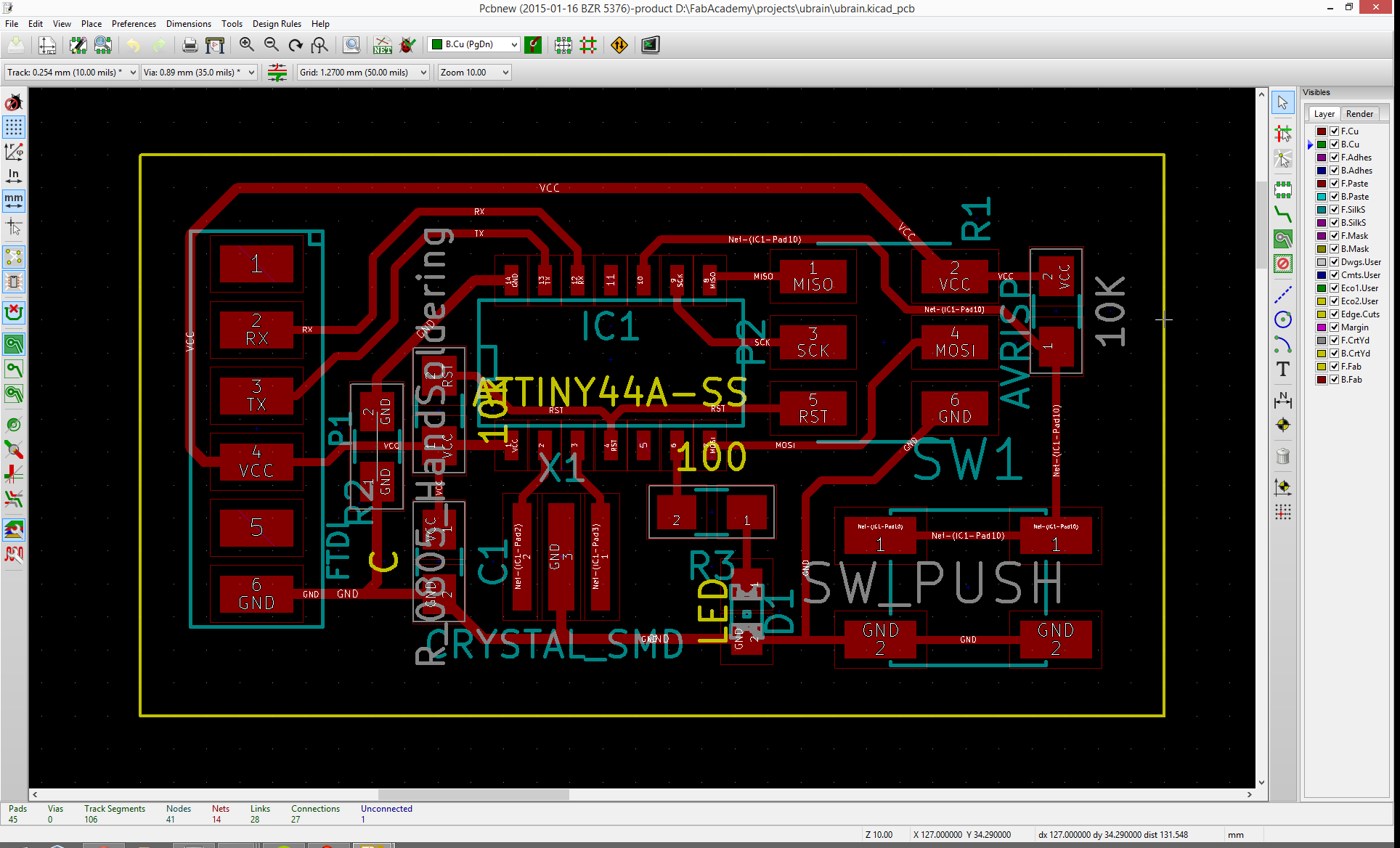
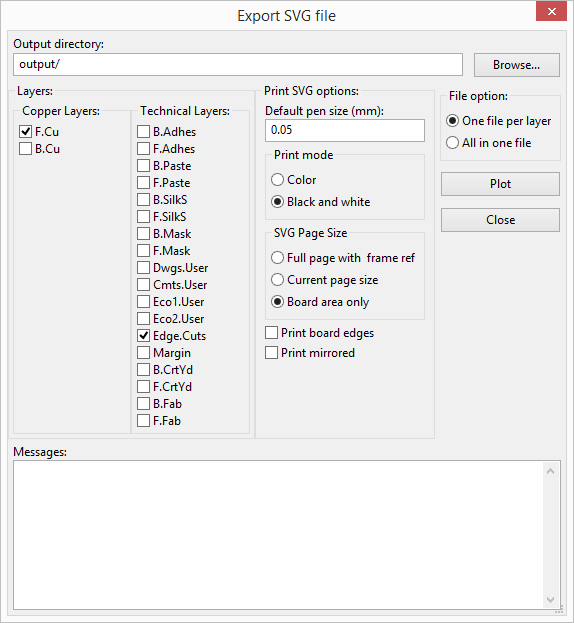
One nice thing that just seemed to work was exporting to get it into fab modules. You can directly export from the pcb editor as a SVG which worked quite well. One trap was to make sure that you don't have any hidden text going over the board edges as that will make the exported board area bigger than needed.
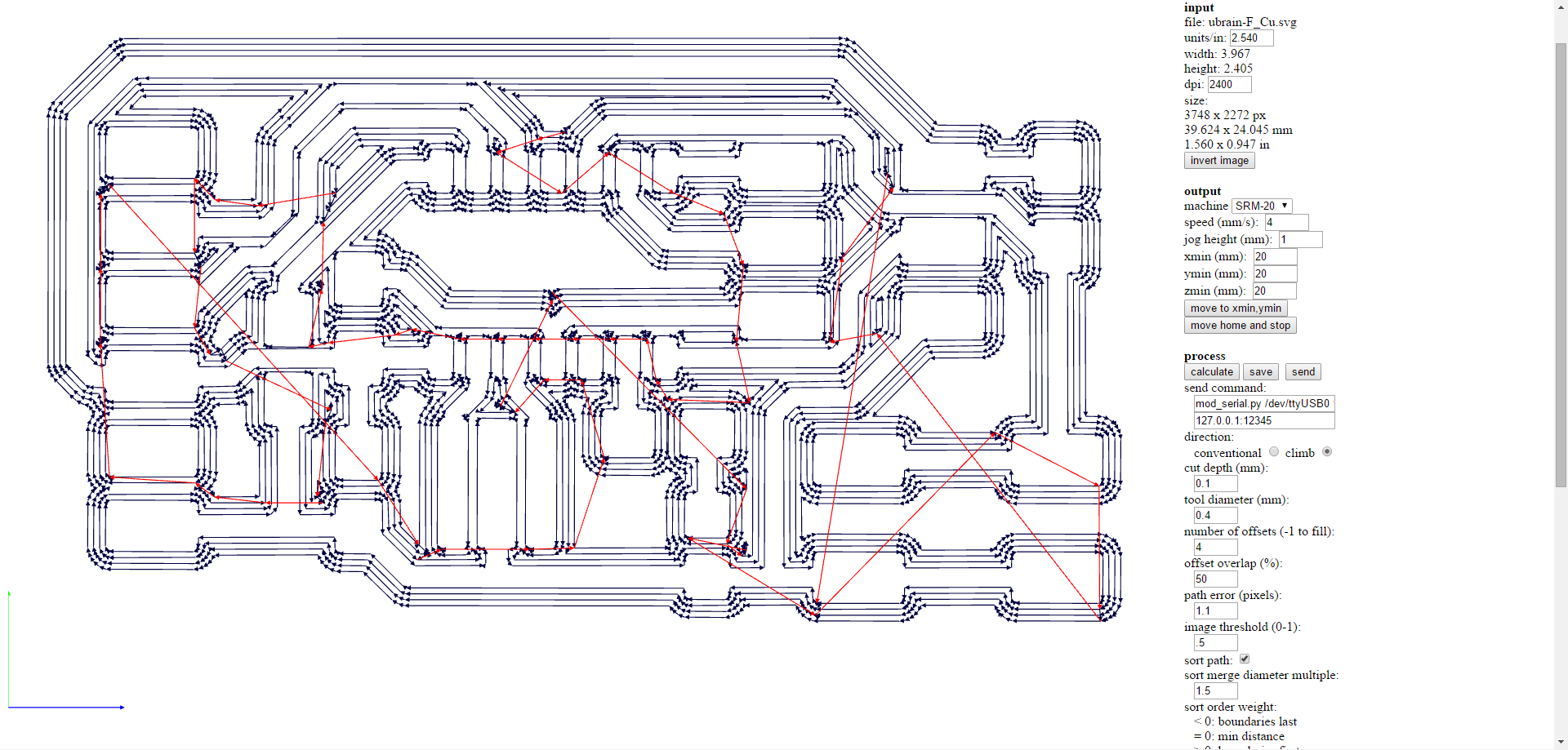
From there is was back into fab modules, rather than converting the svgs to pngs I just loaded the svg files directly. I found 2400 dpi worked quite well for generating clean toolpaths.
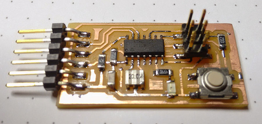
After milling and stuffing I now have a small board ready for embedded programming next week.