7. Electronics design
This week I learnt to design and manufacture simple boards.
Design
In order to fabricate any kind of board we first need to draw a schematic, this will be a graphic representation of the components in the board and how they are connected.
We decided to use the next design as a guide. Although one of our instrcutors modified the design a little. We used KiCad for this step.
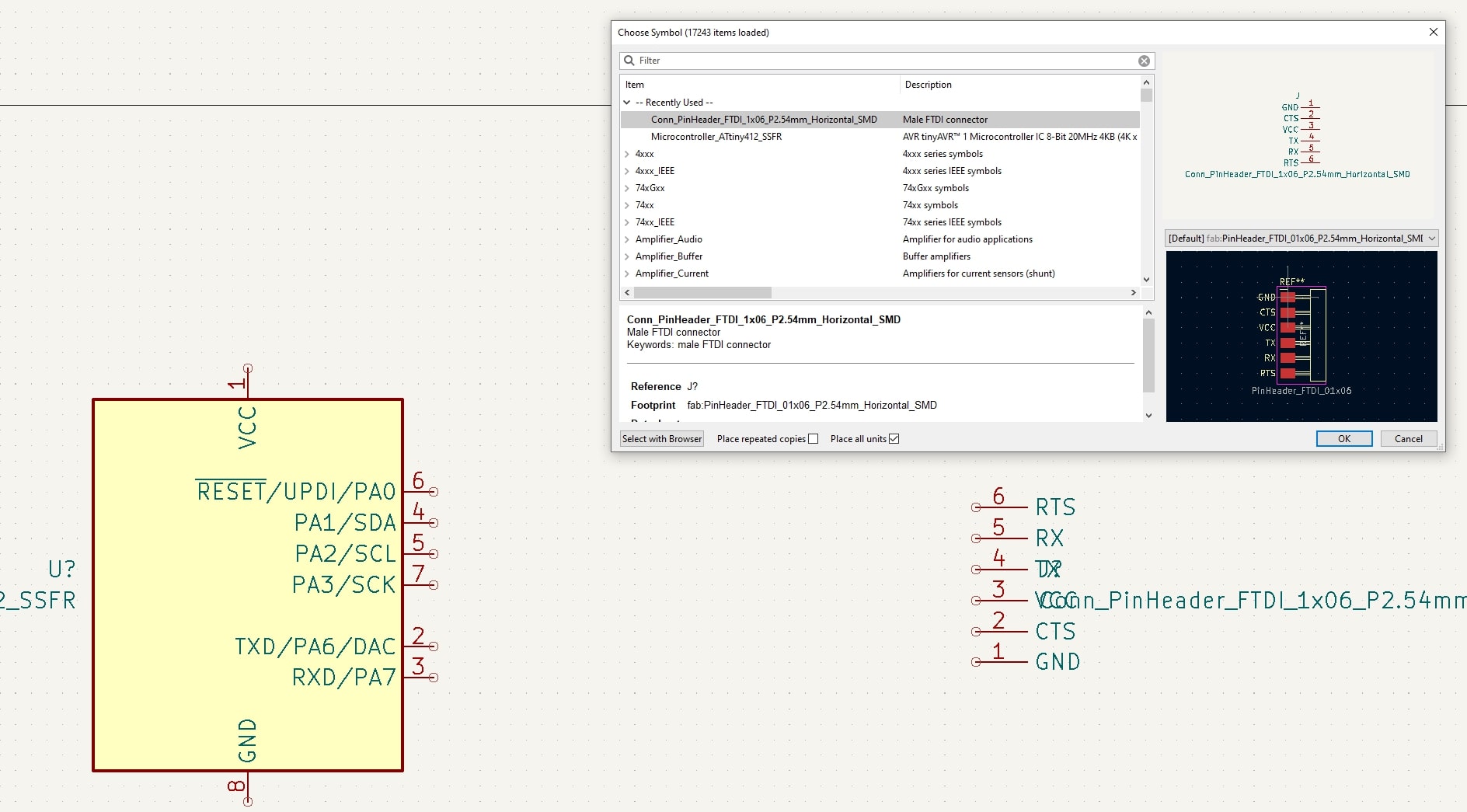
The first step is to add the necessary library that containts all the components in FabLab. It can be found here (as a .zip), or here.
I used the zip file. It can be added under Preferences > Manage Symbol Libraries > add fab.kicad_sym as symbol library
All the components placed:
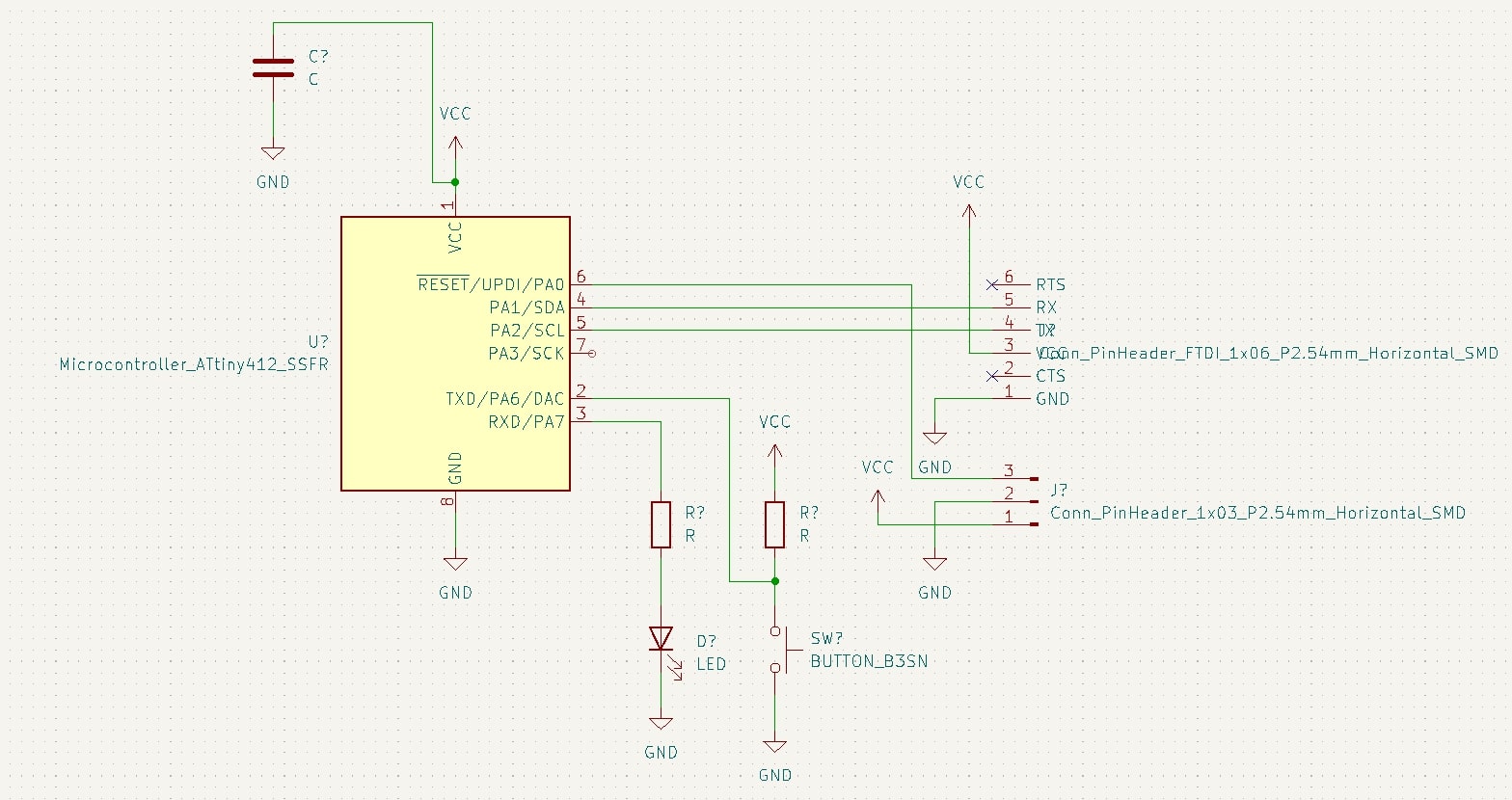
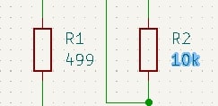
The values of the components have to be modified to fit our design.
 .
.
Once we have a schematic, we can proceed to design the actual board and all of its electrical connections. At first KiCad will only show the components connected using thin yellow lines, this will show us the most efficient way to connect them.
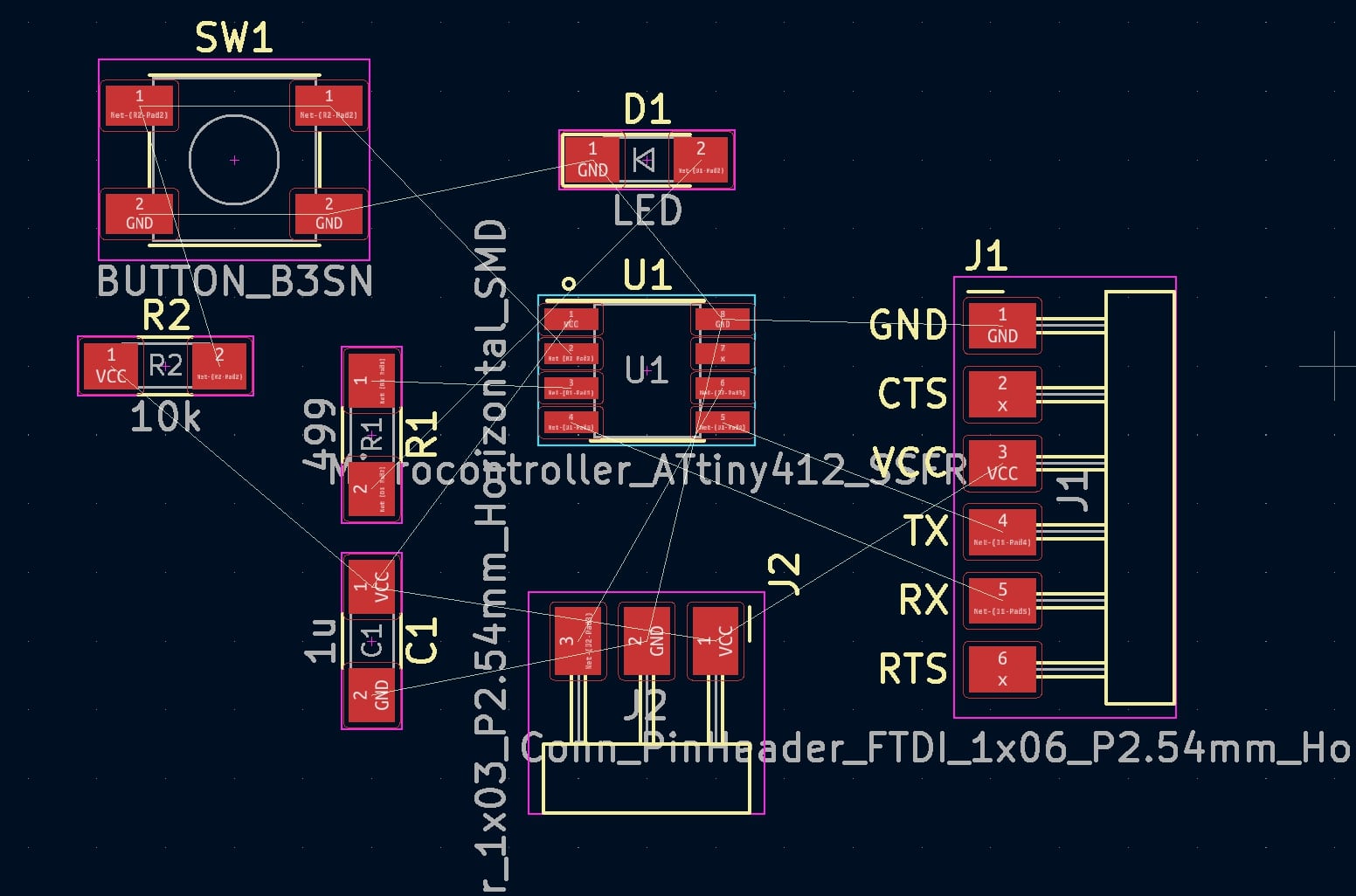
The traces were drawn, this was a little bit of a problem as it is almost like a puzzle where we find to have a way to connect everything together without traces overlapping.
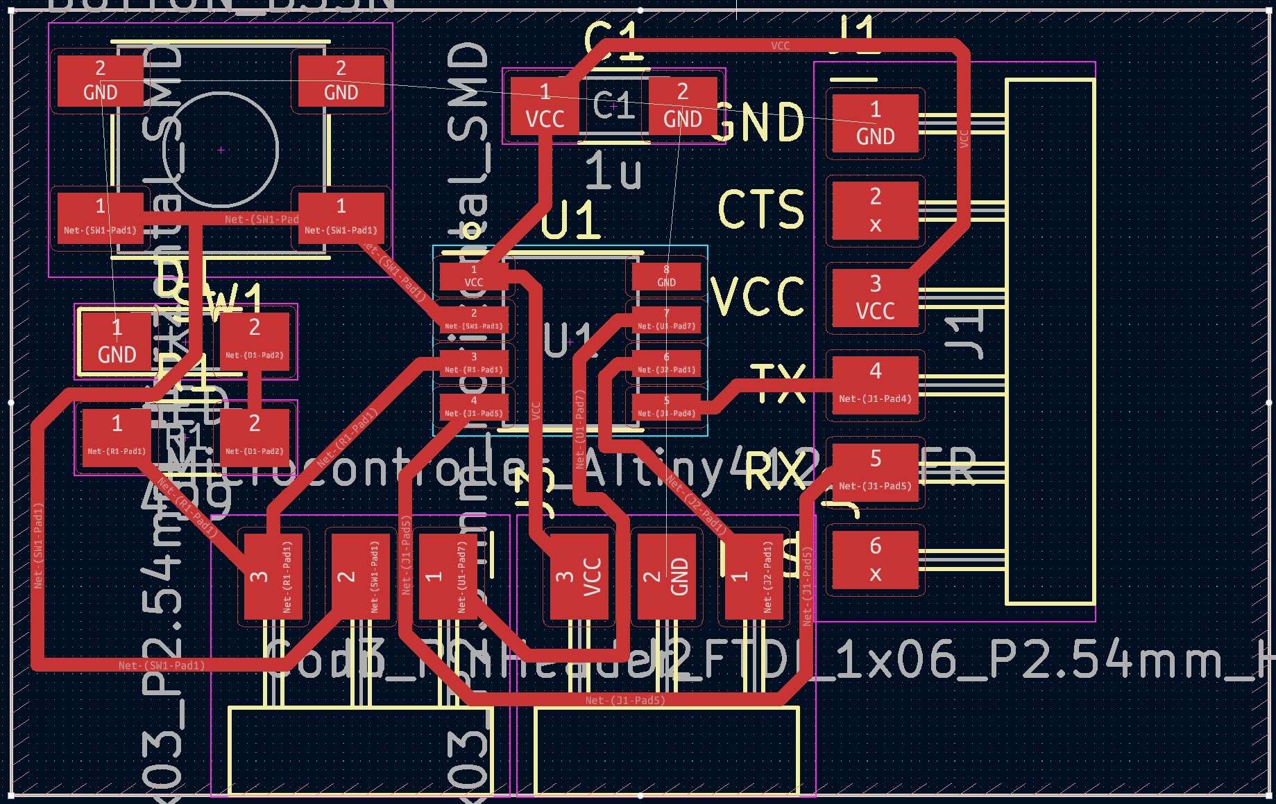
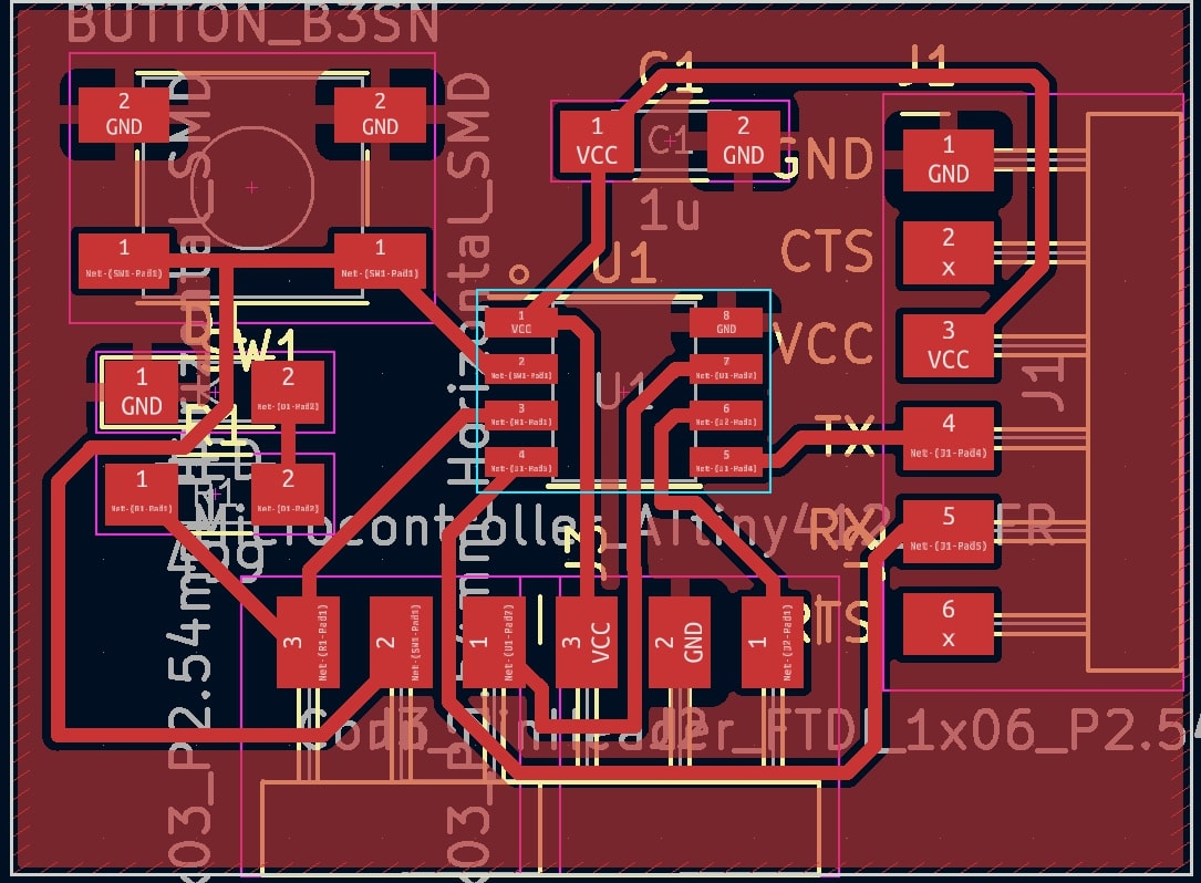
Once the traces are placed we can cover the whole layer in copper to serve as the ground place.
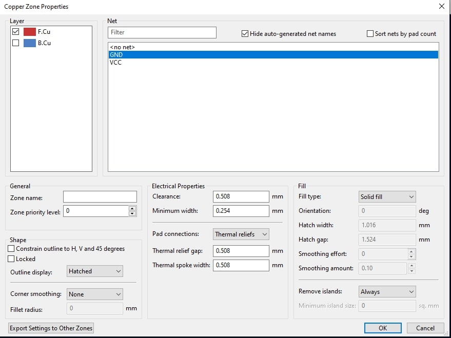
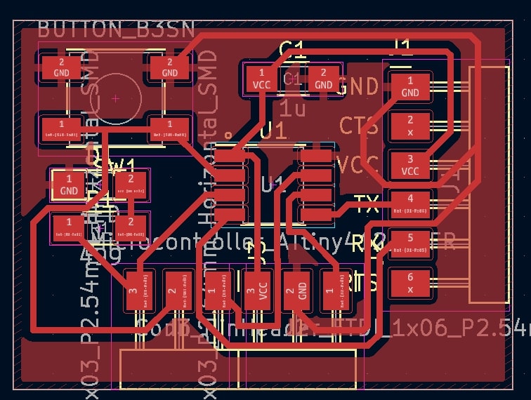
I had to connect some of the ground pins using regular traces because I didn’t know I could just change the parameters for the copper filling, but once I did, I obtained a much cleaner result.
Fabrication
Milling
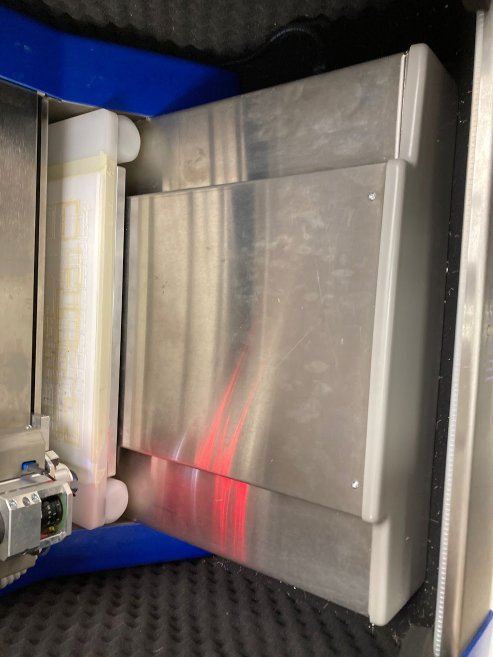
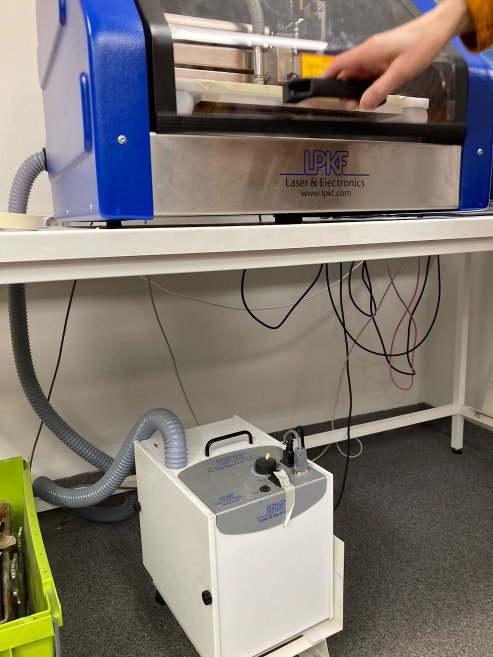
We made the board using the LPKF machine in our Lab. It is a fairly simple process which requires only some calibration (which can be done using only software). The furst step, of course is to place the plate in the machine.
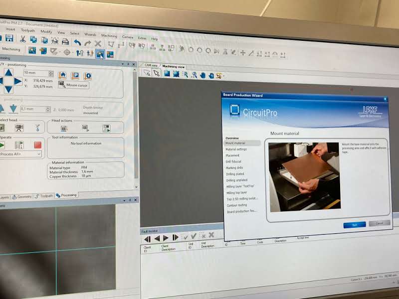
It diesn’t require any kind ofspecial fixture other than some painter’s tape on the edges, as it is secured in place by a vaccuum cleaner.
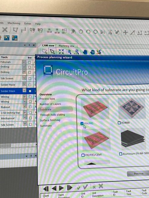
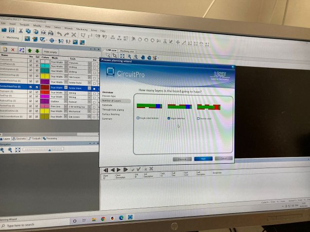
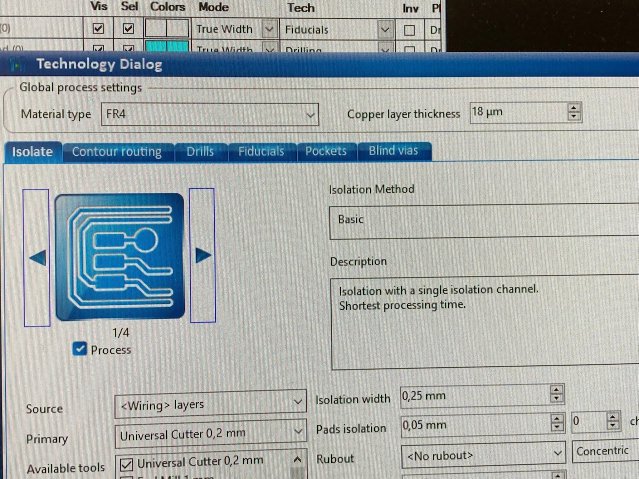
Then we have to specify which kind of plate is to be used and what kind of job will be performed:
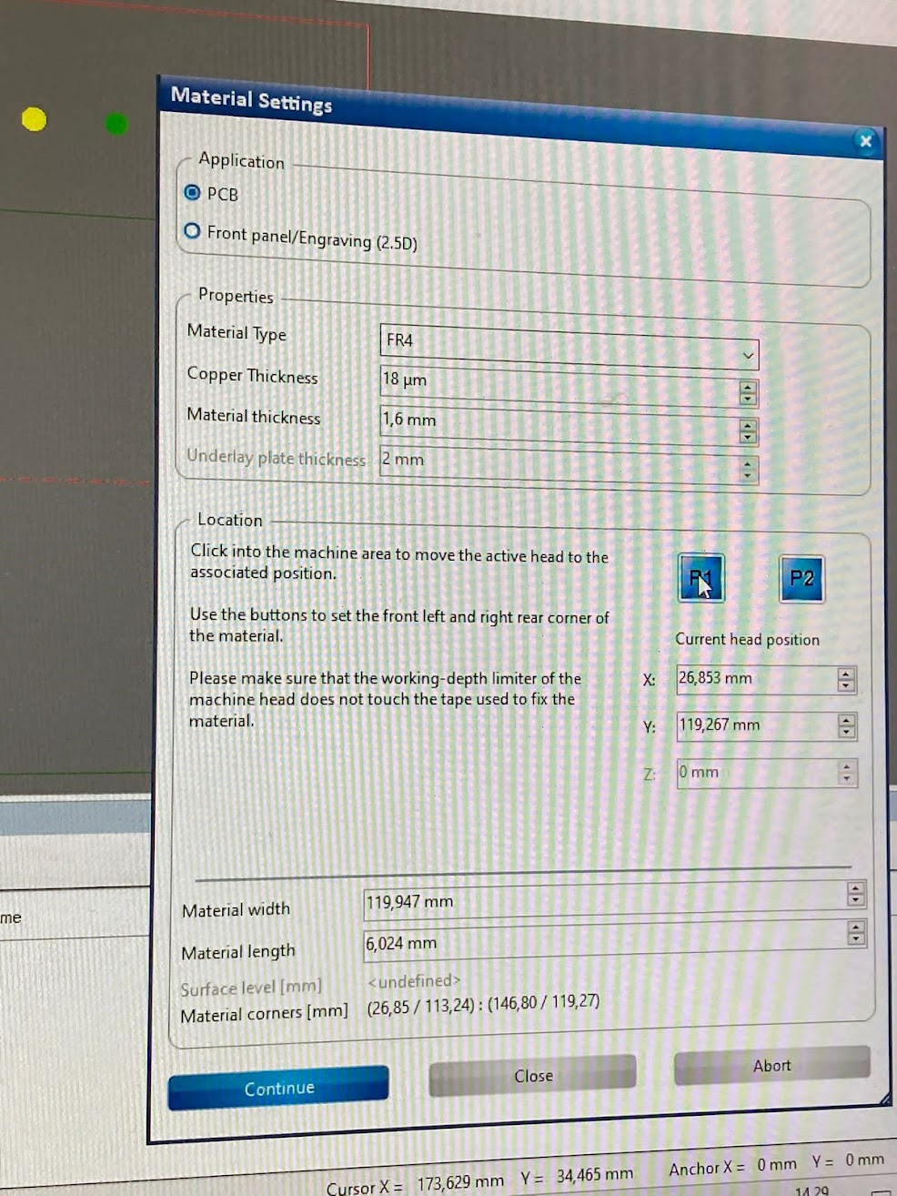
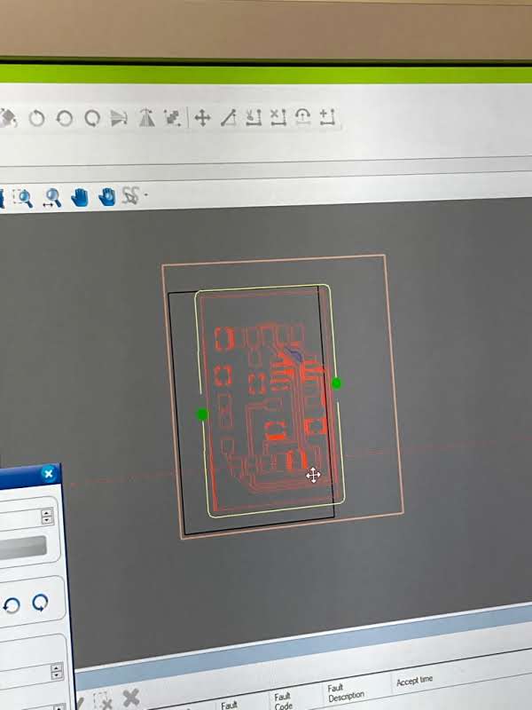
We specify the working area and place the design within it.
Te we specify how much material will be removed:
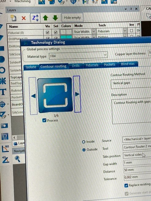
And the type of attachments between the board and the rest of the plate.
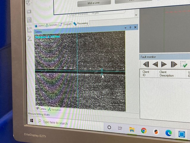
Then a small line is milled onto the board to check it’s the correct width.
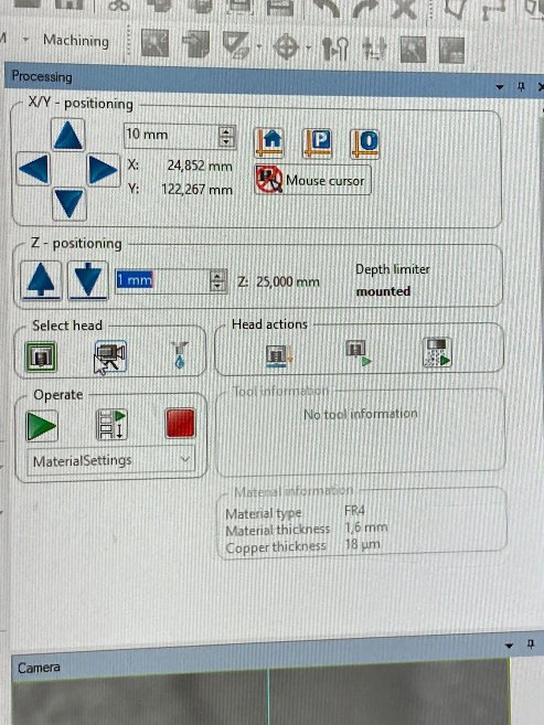
Any adjustments can be made using this menu:
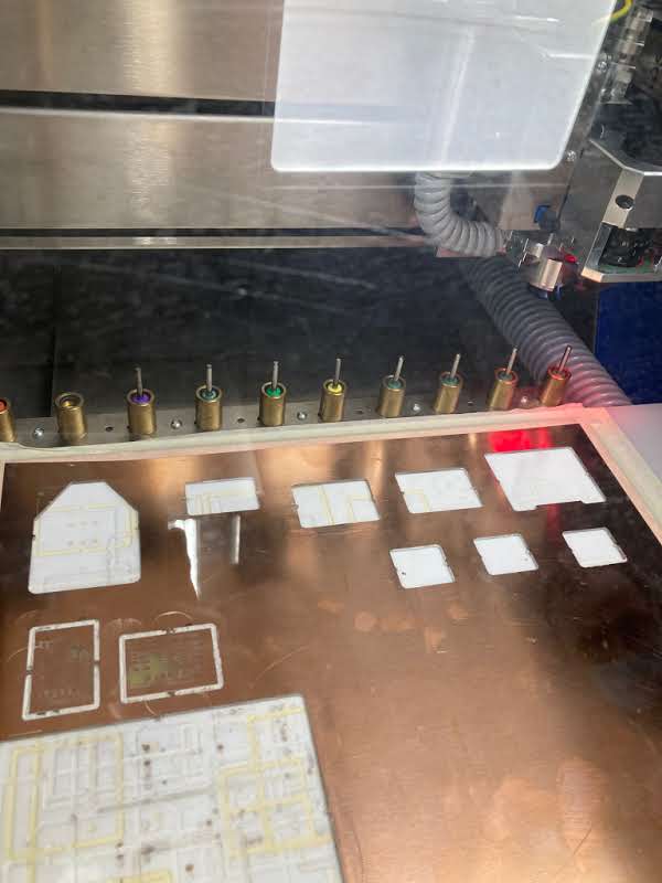
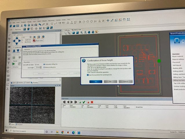
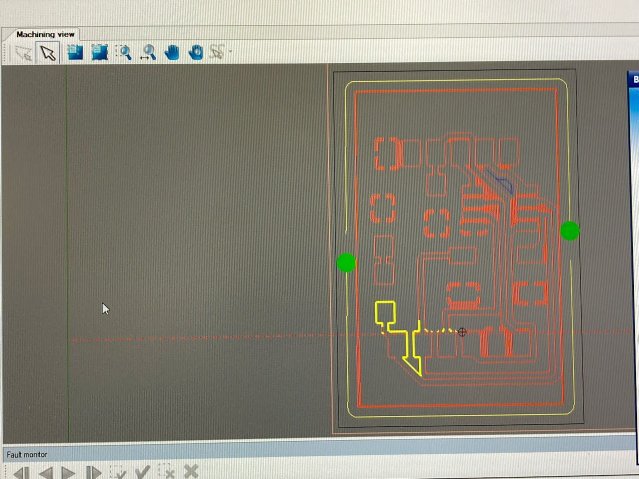
And the the toolpath is calculated:
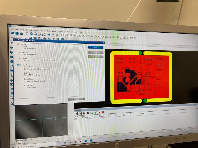
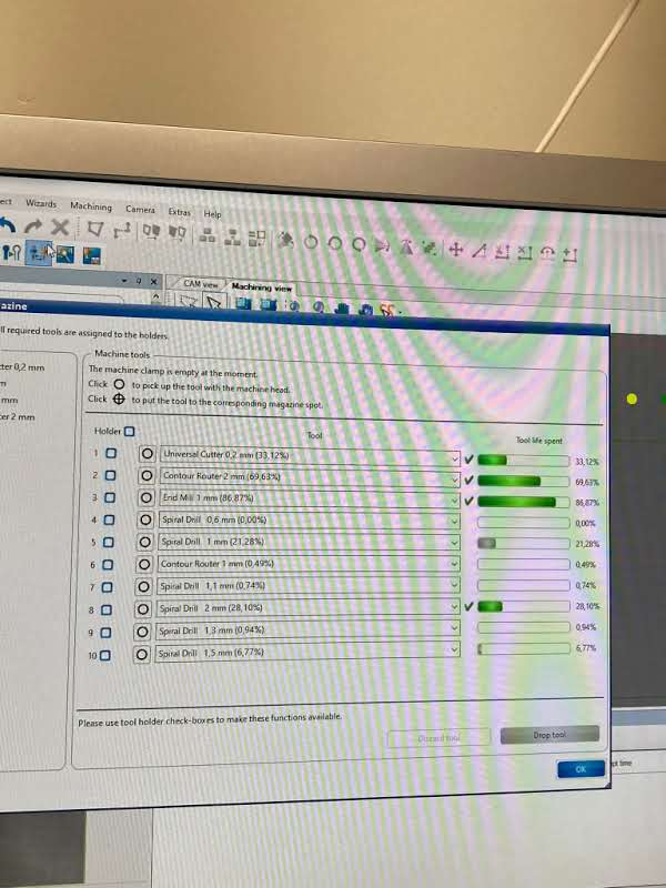
The software even tells us information about the tools’ usage.
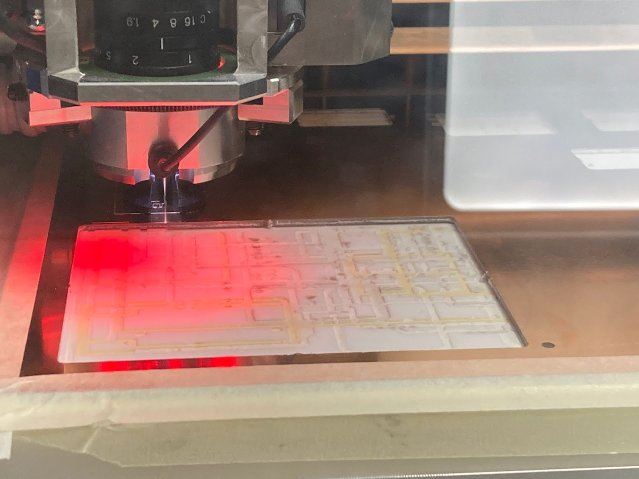
You can see the progress of the job
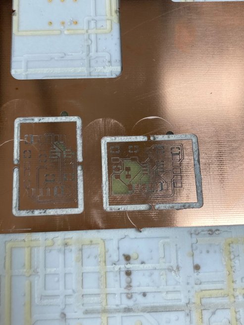
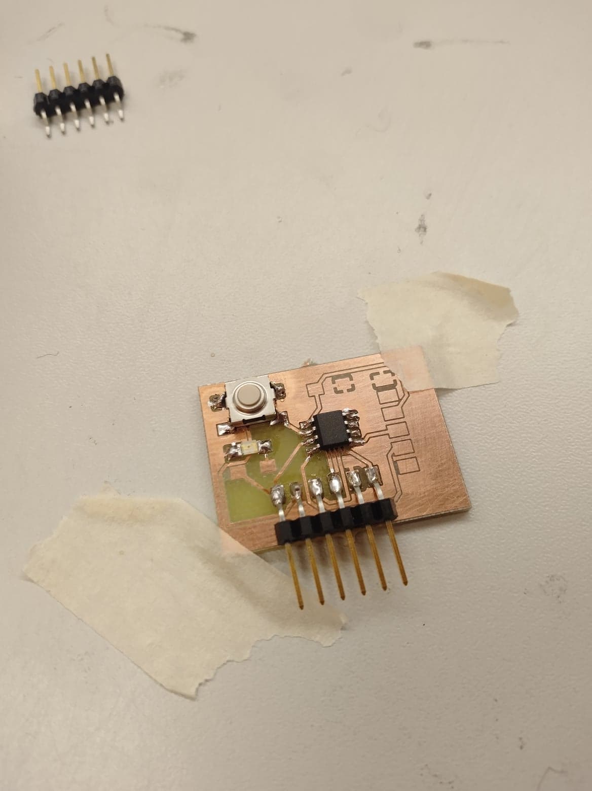
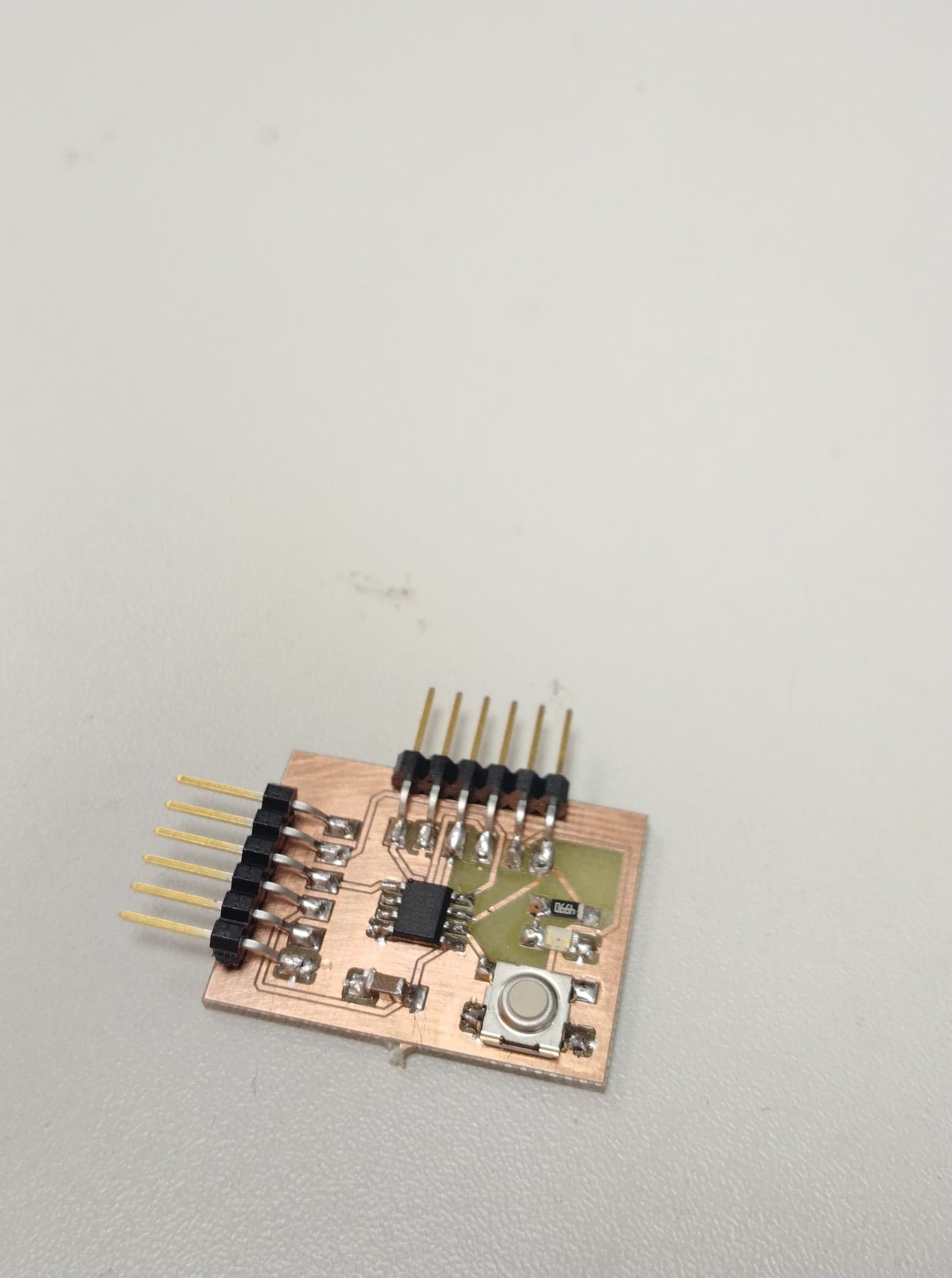
And this is the final result
Soldering
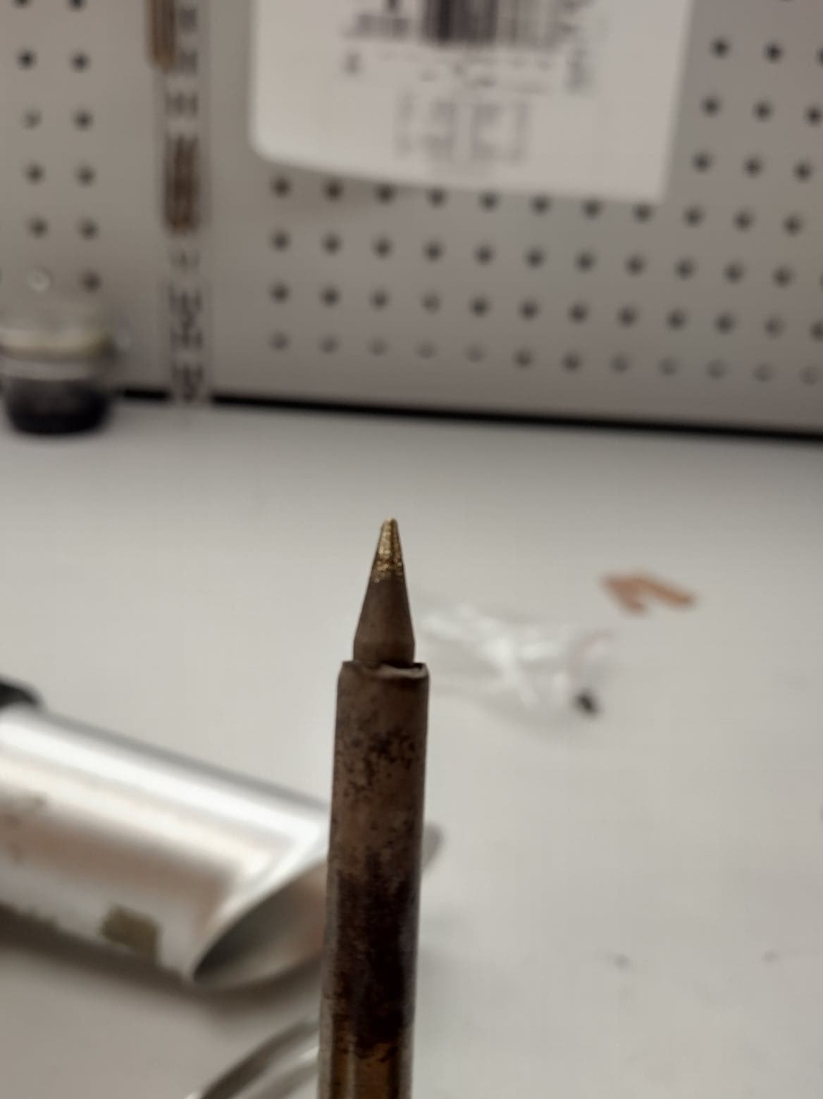
I followed the same steps as when soldering the components for the DPI programmer. Using a clean and shiny soldering iron:
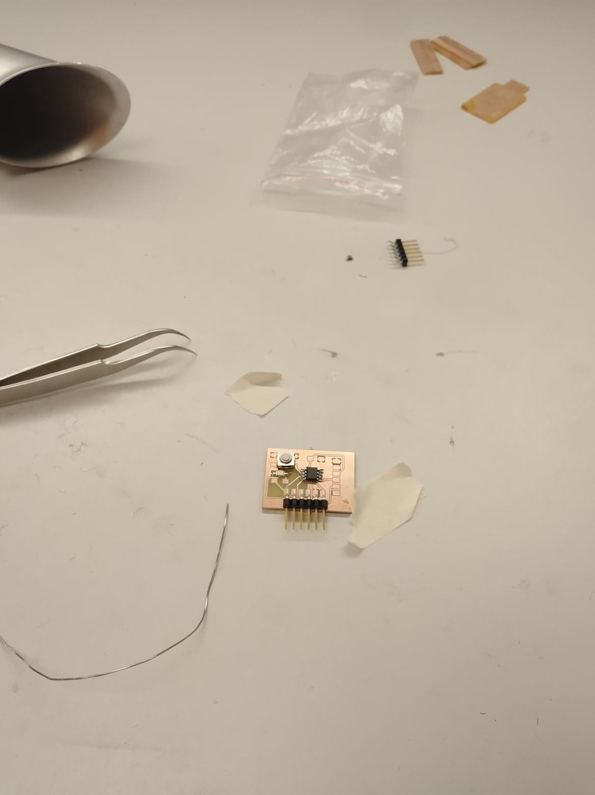
One by one the components were place, although I had a little bit of a problem because the vaccuum sucked a resistor…
Testing
In order to test whether it actually worked, we first had to check if there was any short circuit:
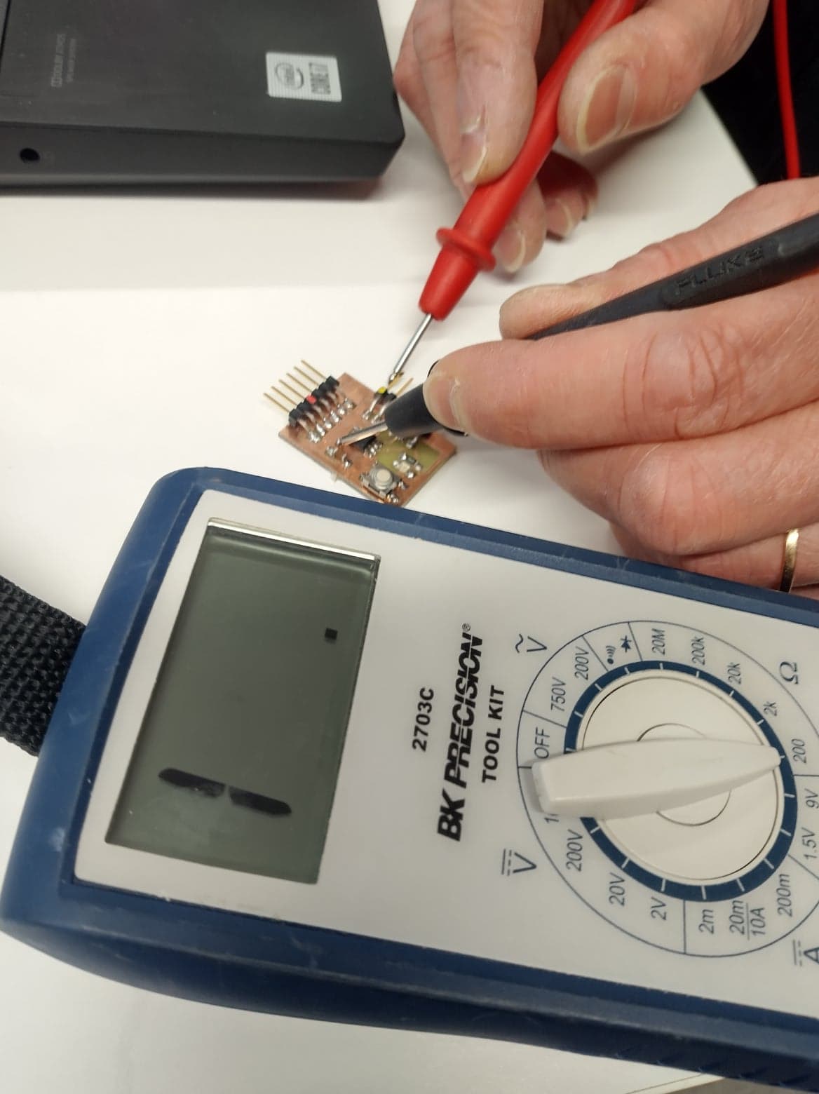
Luckily I soldered everything correctly. Using the UPDI programmer, we uploaded one of Arduino IDE’s programs, which made the LED blink.
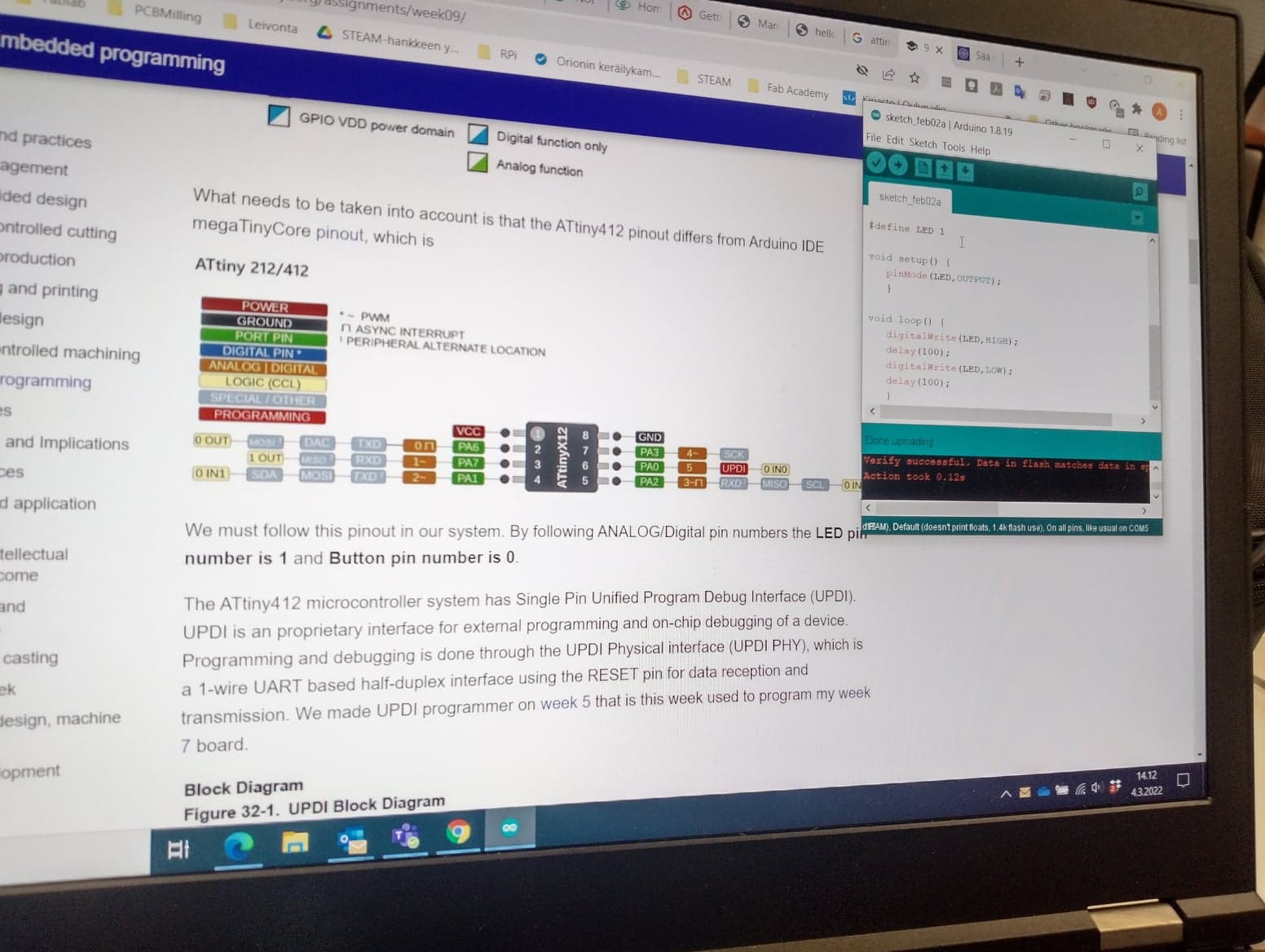
void setup() {
  // initialize digital pin LED_BUILTIN as an output.
  pinMode(PA7, OUTPUT);
}

// the loop function runs over and over again forever
void loop() {
  digitalWrite(LED_BUILTIN, HIGH);   // turn the LED on (HIGH is the voltage level)
  delay(1000);                       // wait for a second
  digitalWrite(LED_BUILTIN, LOW);    // turn the LED off by making the voltage LOW
  delay(1000);                       // wait for a second
}
Final result
https://youtube.com/shorts/ilHSweNDTtQ