5. Electronics production
This week I learnt to make circuit boards by milling them.
Design
It was decided that we were going to make a UPDI USB-D11C programmer, the first thing we needed was an image of the circuit and a frame to remove it from the rest ofthe board. The images should be preferably .pngor .svgfiles, as they preserve th most detail. In pur case they look something like this:

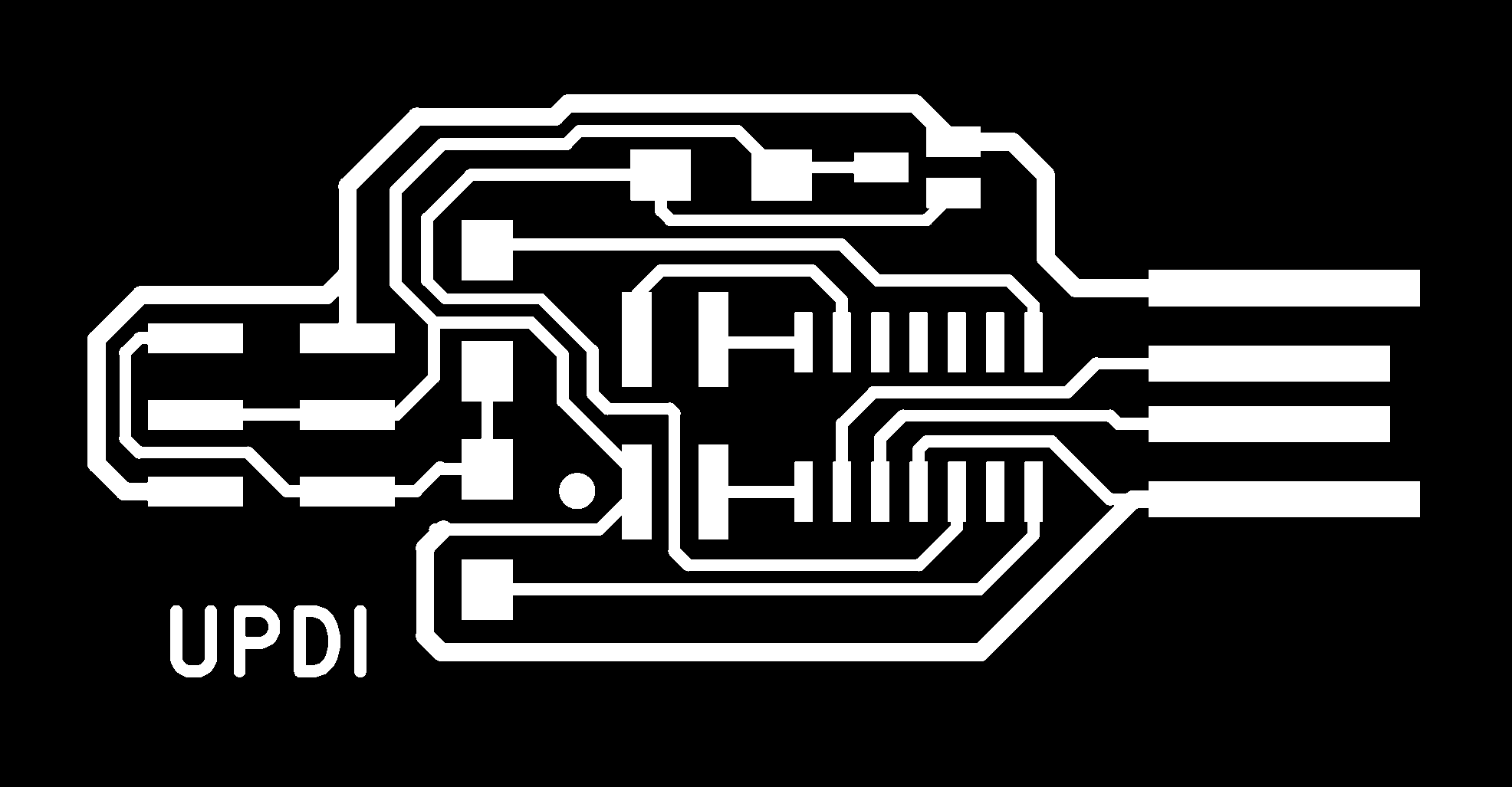
The pictures above are
.png,svg’s are on the bottom of the page.svg’s don’t display properly
In order to get a file we can use to actually mill the board I used mods.cba.mit.edu, which allows to create a .rml (machining) file. First step is to add a workflow, which can be done by right click > programs > open server program > machines > Roland SRM-20 > PCB png You should select the svg option if you are using such file.
I upoaded the file containing the traces of the circuit. This contraption considers white color as copper and black as the areas to mill, so in this case I inverted the colors. At the bottom left the origin should be set to x = 0, y = 0, z = 0, otherwise the drill will be floating. The screen should look like this:

For milling the traces I used the mill traces workflow with a tool diameter of 0.2mm (V-bit), cut depth and max depth of 0.08mm, the other parameters were left untouched. After calculating and automatically saving the resulting file, I got this:

** Notice: The red lines are the places where the drill stops touching the board to be able to move**
Using the same file I used an offset number of 0, now using a 1mm diameter tool, which will remove the rest of the copper, this is the resulting file:

For miling the outlone I used the mill outline workflow, I used a cut depth of 0.6mm and a max depth of 1.7mm, which corresponds to the thickness of the board, this was to be able to remove it from the rest of the plate.

Fabrication
The detailed workflow can be found at the group assignment page. For the first files (traces), the first couple runs gave quite uneven results, but that is to be expected when using a V-tip, as you can see the traces were not very well defined at first. This is because at the beginning only the top of the bit touches the copper, and so the Z coordinates needs to be adjusted until the diameter of the material removed matches with the value used in mods.

And after a couple tries:

The the excess copper was to be removed, in order to prevent a potential short circuit; and the programmer was taken out of the plate using the third file (The frame of the programmer).

Soldering the components
Using a nice and shiny iron

As you can clearly see, my soldering skills are not the best by any means, but at least they did the job.


Programming the programmer
At this point, the programmer is basically just a bunch of semiconductors in a plate. In order to be able to actually program something with it, we first have to burn the bootloader, which will basically let it know it’s a programmer.
Ironically to do this, we need another programmer. Who had the first programmer?

Our instructor Gleb helped us do this.

And then to test it a simple program that echoed everything it received through serial.

I was technically not supposed to do this yet, but you can see the detailed process of how to do it here
Files
Used to mill the traces in the board
Removes unnecesary copper.
Removes the board from the crcuit blank.