7. Electronics design
This week I explored electronics design and worked on the following assignments.
Group assignment
- use the test equipment in your lab to observe the operation of a microcontroller circuit board
Individual assignment
- redraw an echo hello-world board,
- add (at least) a button and LED (with current-limiting resistor)
- check the design rules, make it, and test it
- extra credit: simulate its operation
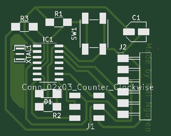
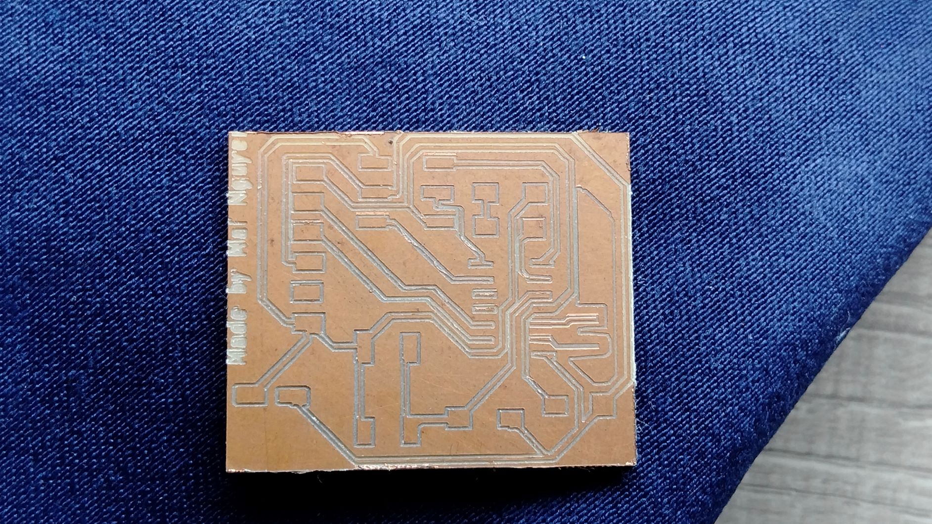
Hero shot of the week
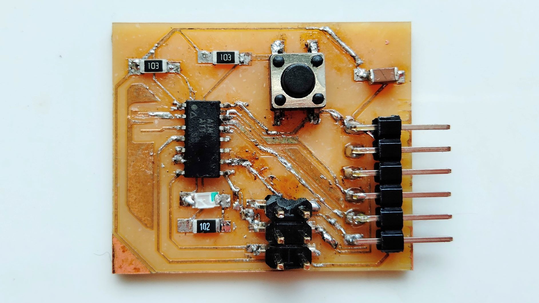 My very first self-designed, CNC-milled and half-handmade circuit board

Group assignment
I started using both oscilloscope and multimeters during my third year at university so I am quite familiar with them.
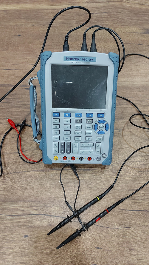
Oscilloscope
Our lab has a handheld Hantek DSO8060. It supports 2 input channels up to 60MHz.
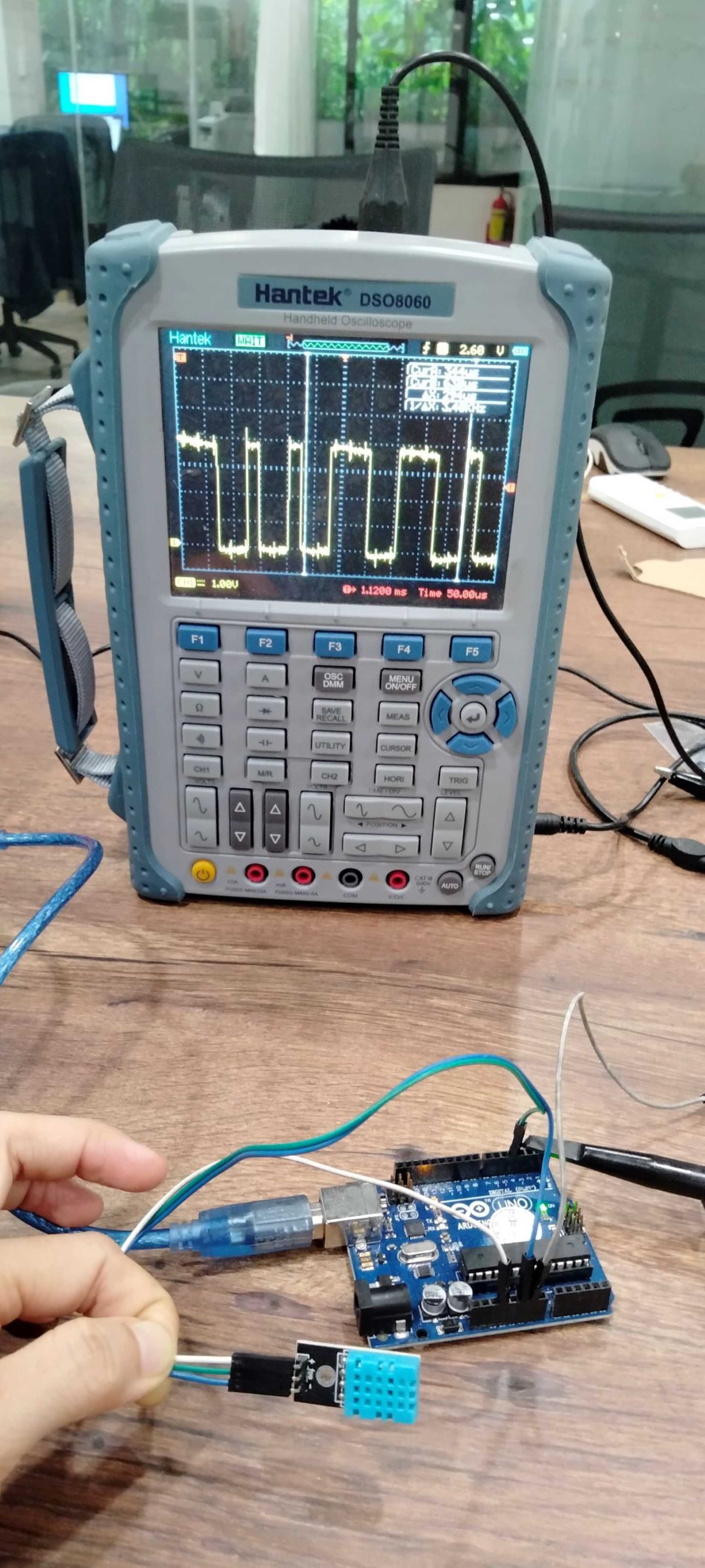
To observe the signal output by a temperature sensor connected to an Arduino Uno on this oscilloscope, I hooked channel 1 to the digital output pin of the sensor, and clipped the aligator clip to the ground connection of the Arduino. I then adjusted the trigger level and pressed the TIME/DIV sine wave button until a nice and clear image of the signal appeared on the screen.
Individual assignment
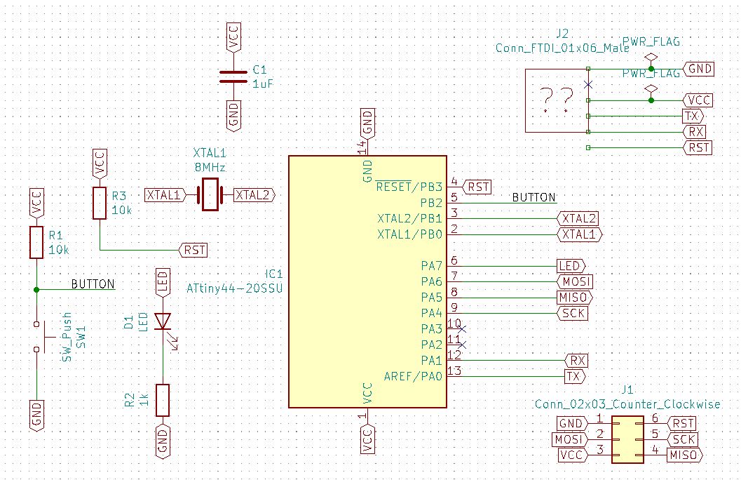
I finally found a local supplier for Attiny44A-SSU chips and ordered a handful of them. The board I will be making is FTDI type
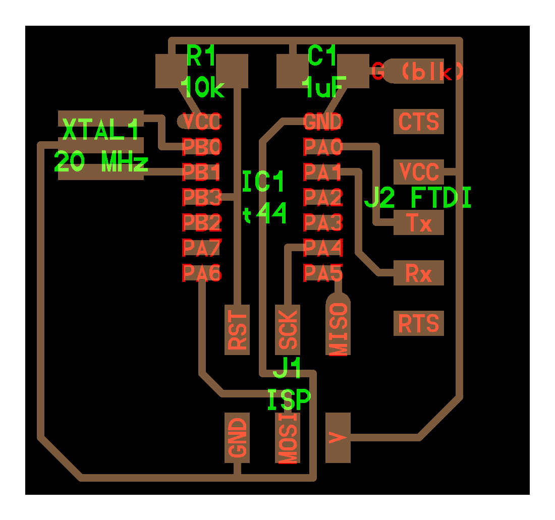
Preparing the components
Here is our exciting menu
- Microcontroller ATtiny44A
- Capacitor (1uF)
- 8MHz crystal
- Resistor (10k)
- Resistor (1k)
- Button (6mm switch)
- LED (white)
- FTDI header
- 2x3-pin header
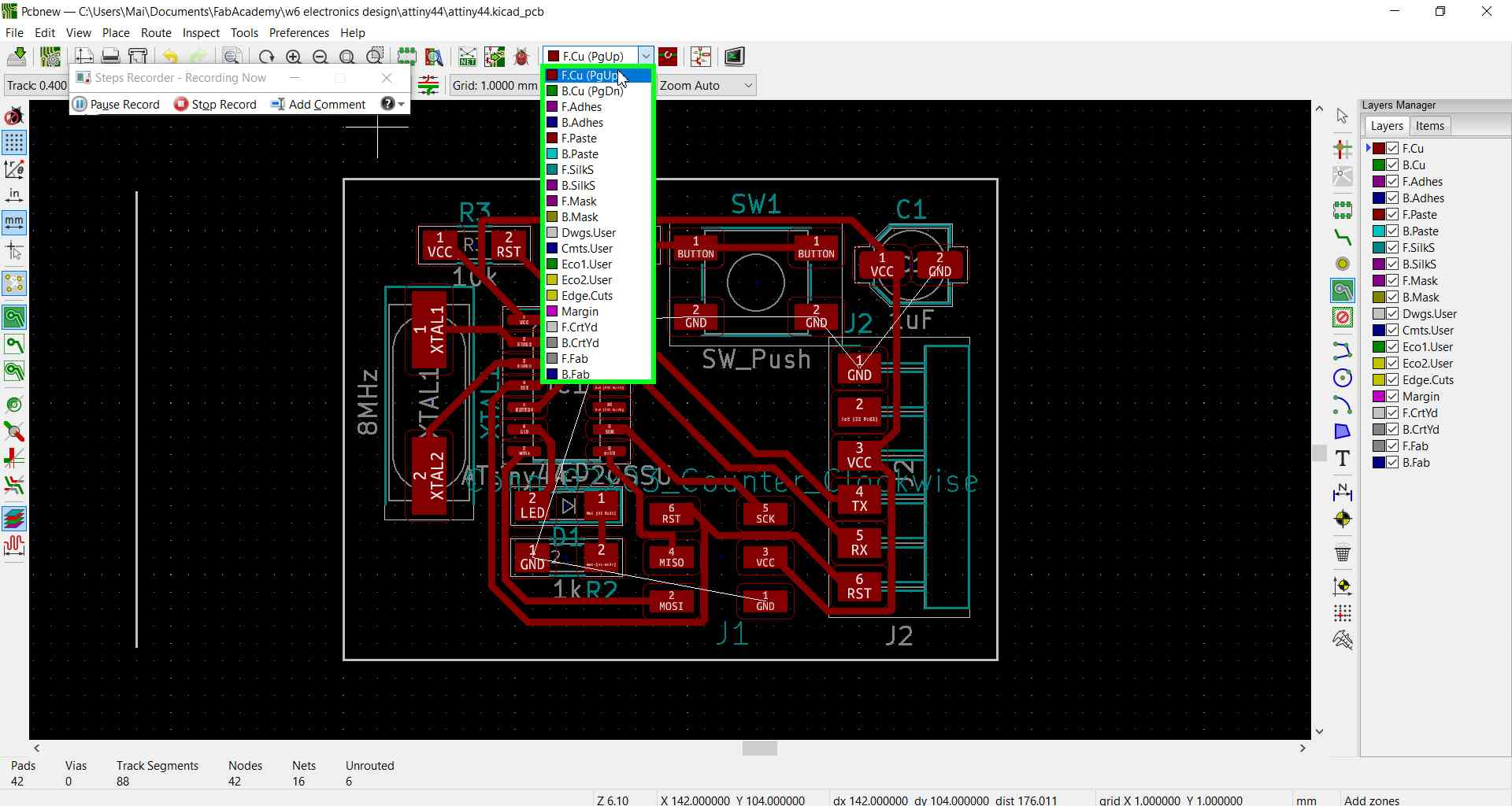
Installing KiCAD and poking around
First I downloaded and installed KiCAD.
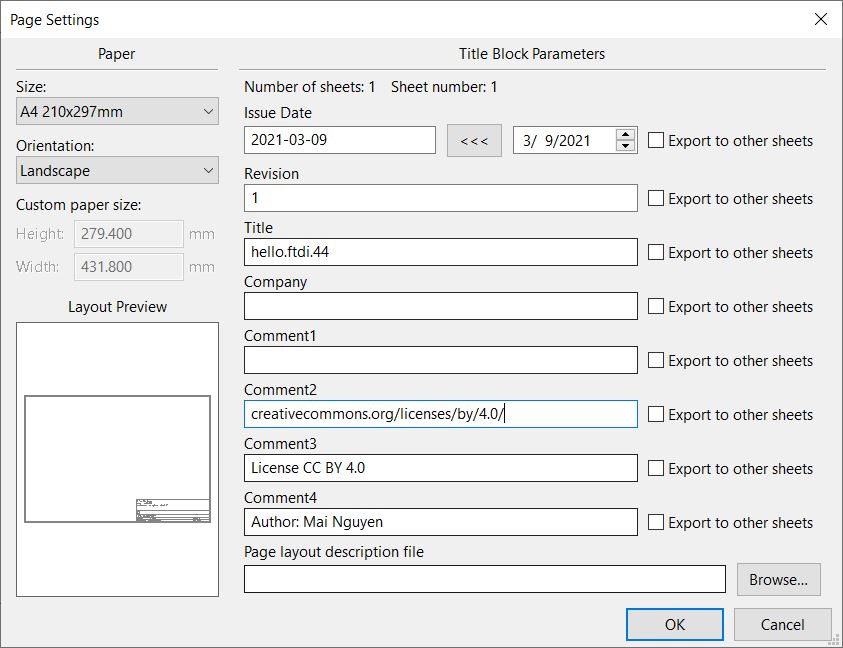
I went to Page settings and fill in the following information
Adding components
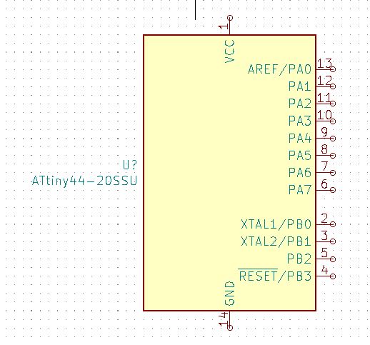
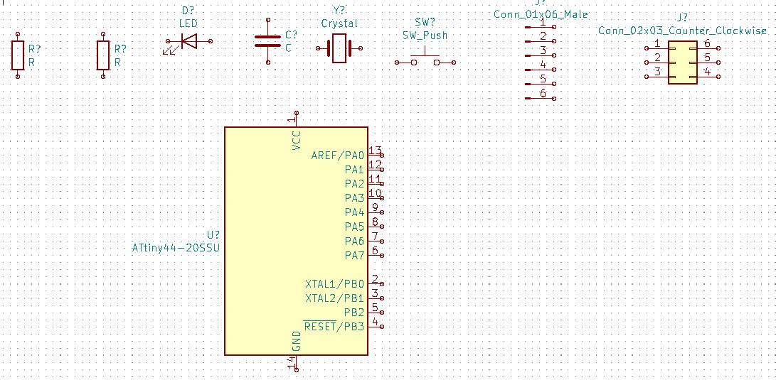
Place a component by typing attiny in the search field and selecting Attiny44A-SSU.

Edit connector
Below is a photo of all my component acquisitions.
We will now proceed to specify details for each component.
Editing components
By right clicking on a component, you will see Edit value and Edit reference.
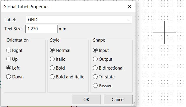
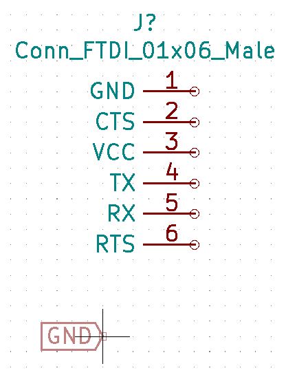
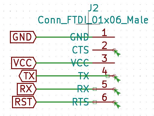
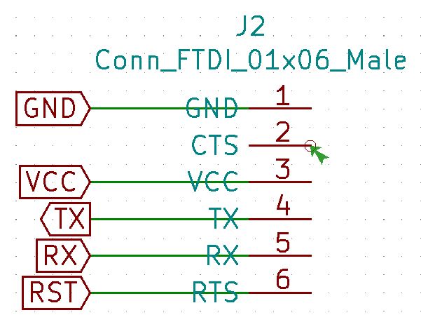
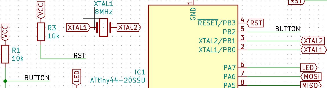
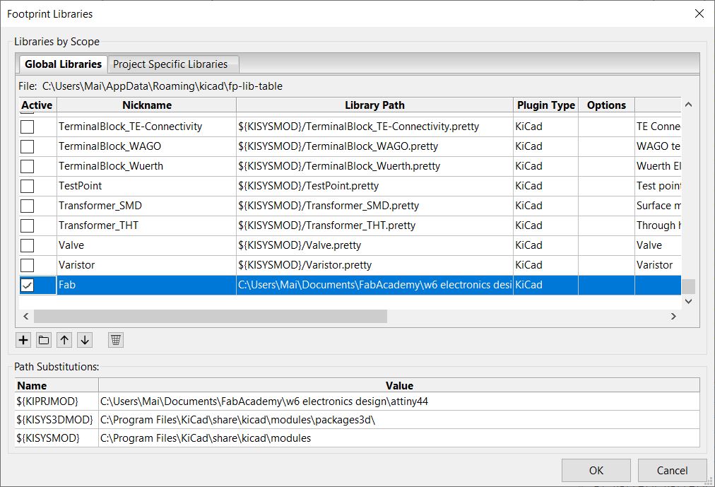
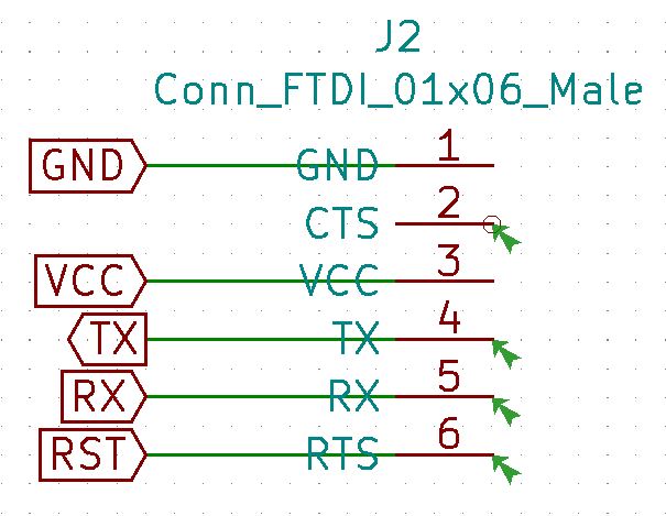
At this point, I wanted to label the pins of the FTDI connector. I tried placing a global label but it did not turn out the way I wanted (see below). Talking to a fellow student, I decided it was necessary to install the fab library containing all the components relevant to FabAcademy in order to create such an appearance.
Adding the fab library to KiCAD is a quick and easy process. To do that, go to Preferences, select Manage Symbol Libraries, add a new row, name it Fab and specify a path to the fab.lib file.
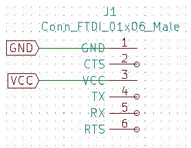
Once the fab library is added, I can straightaway type FTDI in the component list and select conn_FTDI. Et voila, now the header looks exactly how I want it to be.

Annotating components
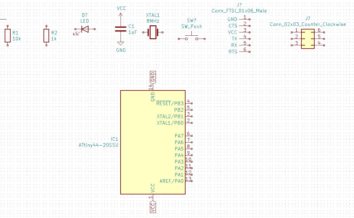
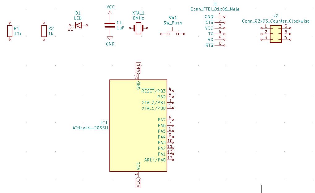
If you notice, the components still have a ? to their names. We can remove that by annotating them. The software will assign letter, followed by a number for every component. Resistors will be Rx, capacitors Cx, LEDs Dx, connectors Jx and so on.
Before and after annotating:
 Before
 After
After
Connecting components
Electrical Rules Check (and the pain begins)
To check if the connections make sense, I used Perform Electrical Rules Check feature in Eschema.
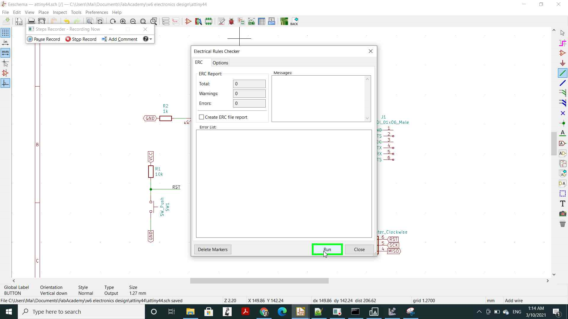
If there are errors, the software will return
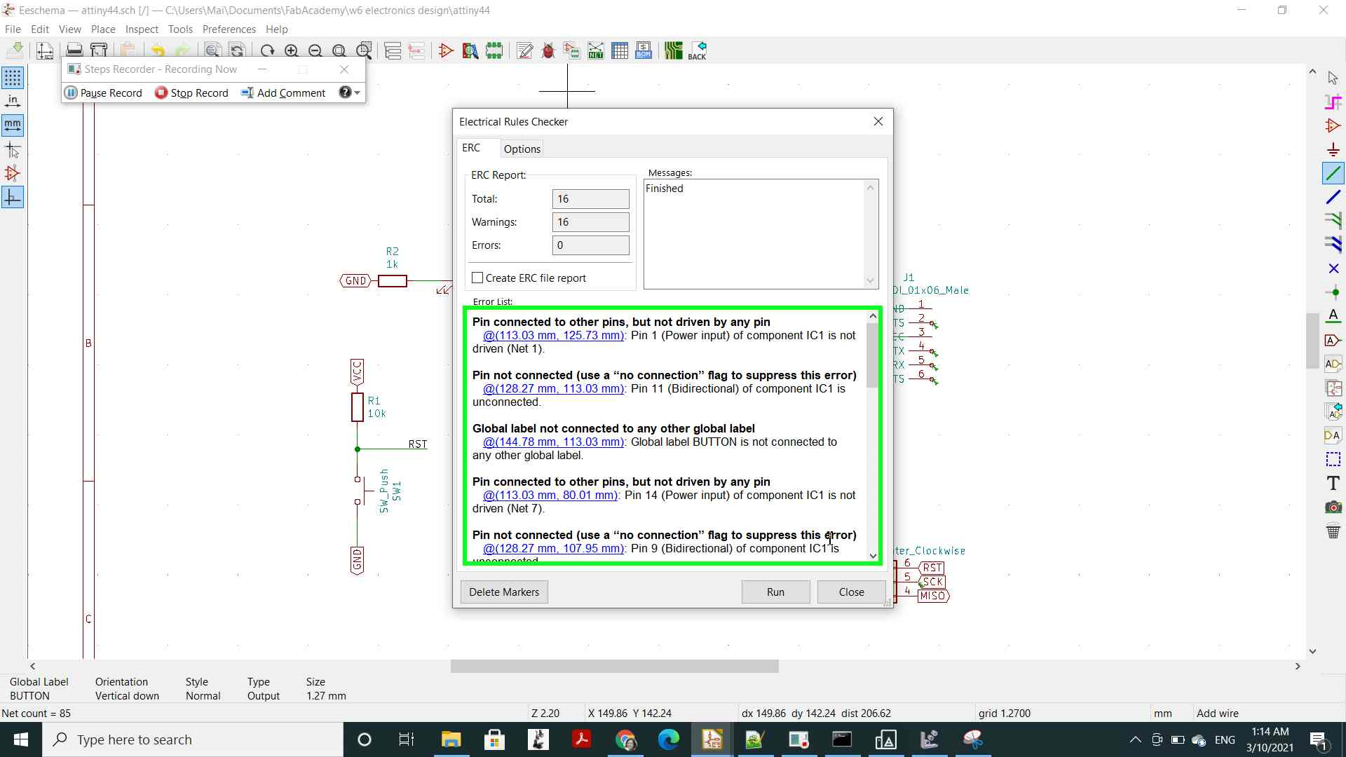
One by one I try to address the warnings until there are no more. This includes
Error 1: Pin not connected (use a “no connection” flag to suppress this error)
Cause: Wires not fully inserted
How to fix: redraw some of the wires to make sure they go all the way to the header holes
Before
After
I also took the opportunity to reverse the wires to the right so the label text is not cut.

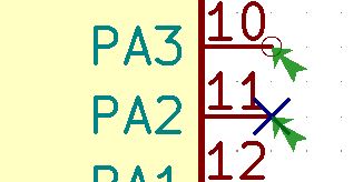
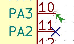
Error 2: Pin not connected (use a “no connection” flag to suppress this error)
Cause: One Button lable is a global label and the other a net label.
How to fix: ensure that labels with the same name are of consistent types. In my case, I changed a Button global label to net type, so that it can be the same as the other Button label.
Before
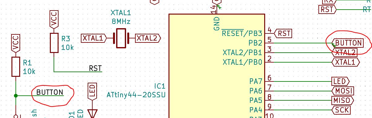
After
Error 3: Pin connected to other pins, but not driven by any pin
Cause: The software does not know where VCC and GND come from
How to fix: Add power flags by clicking Place power port on the right-hand side toolbar.
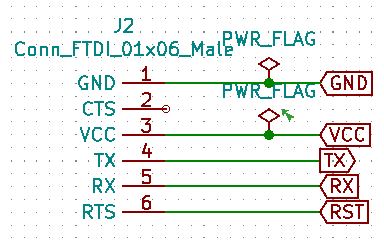
Before

After
I thought I would never live to see this but eventually, I got here. And it barely took 2.5 hours of watching Aalto Fablab’s tutorial, fixing and documenting things as I went. Trust me, you can get here. I feel like I deserve a slice of cake at this point.
When the software is happy, Press Apply, save Schematic and Continue.

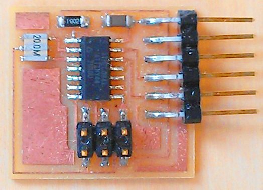
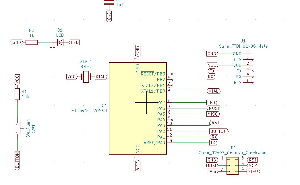
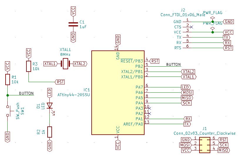
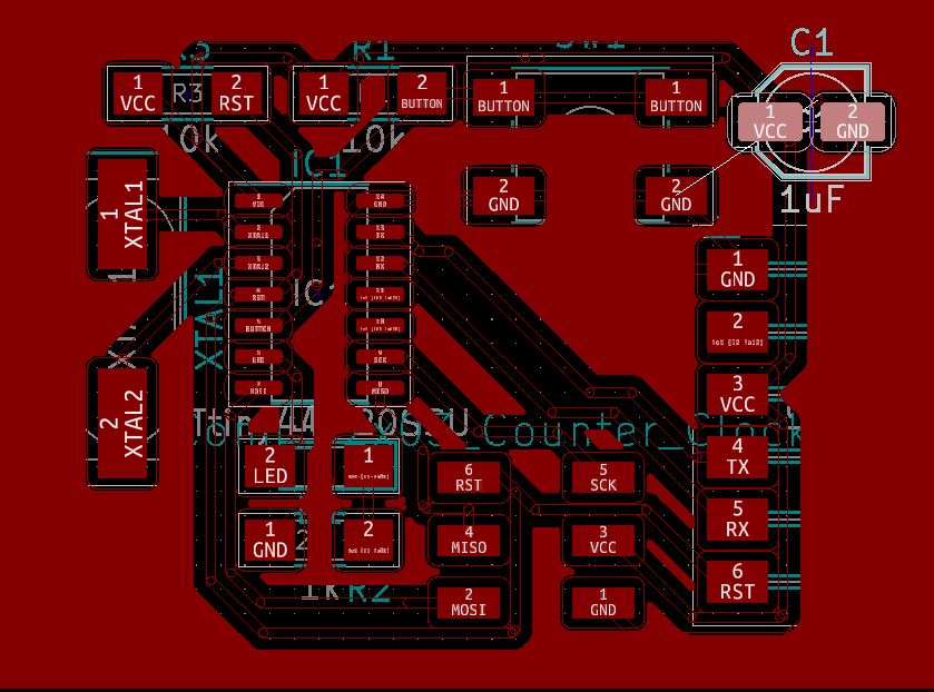
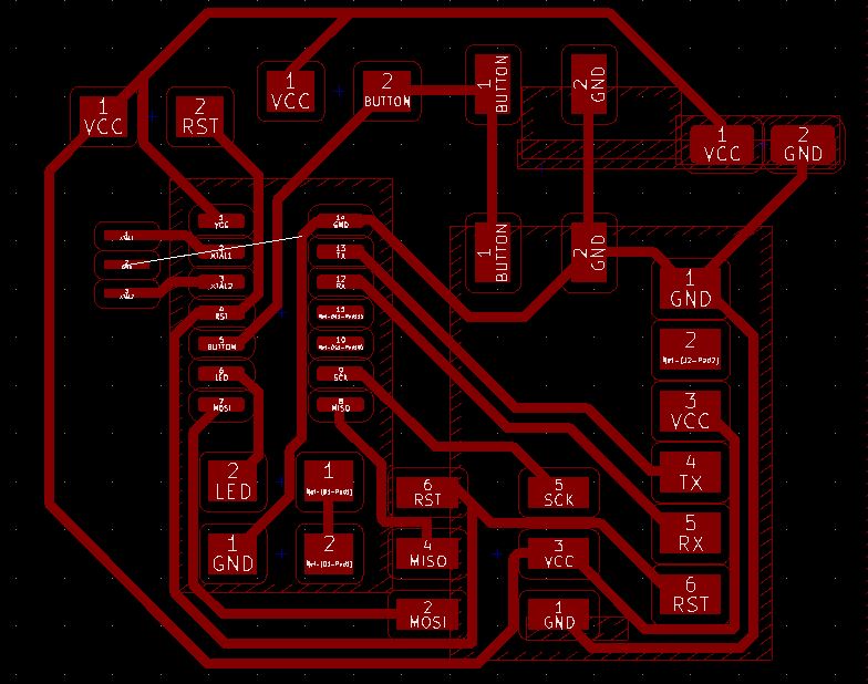
A hero shot of my PCB design at this point
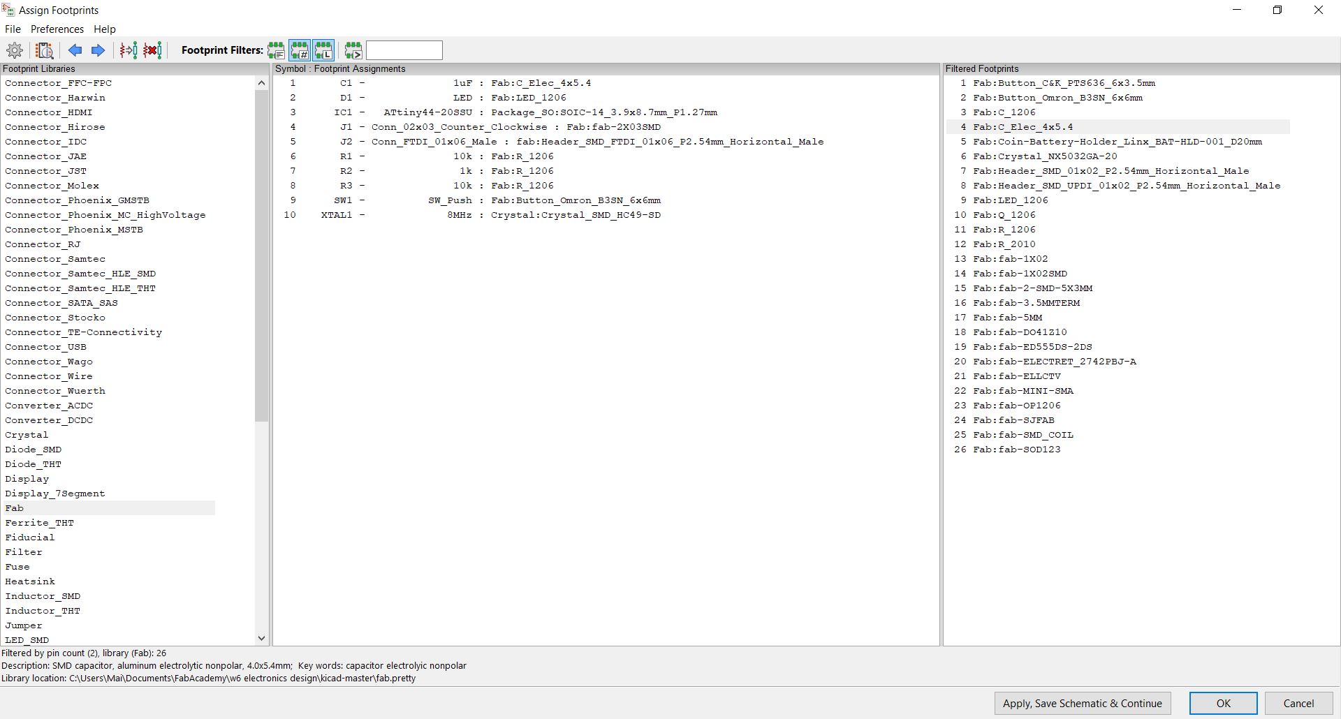
Adding footprints
add global library in order to view footprints
Since I used some components that are not in the Fablab inventory, I had to look for their footprints on my own. Luckily, KiCAD has pretty extensive libraries on their website. I was able to fetch the
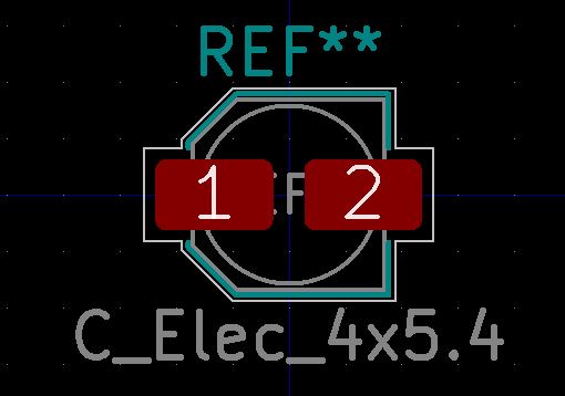
- Capacitor 4mmx5.4mm SMD
- Crystal 8MHz HC49-S SMD
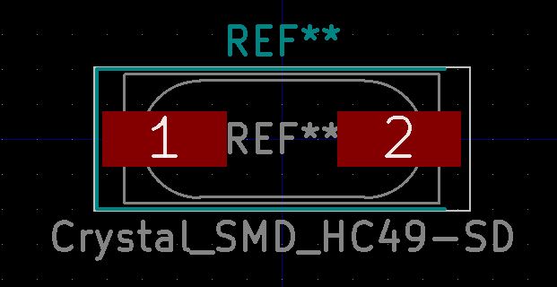
As each library contains many many components, you can just pick the one you need and copy it into the folder fab.pretty. For example, from the capacitor library, I only picked out C_Elec_4x5.4.kicad_mod.
When all footprints have been assigned, press OK
Generate netlist
This step is straightforward. Click Generate netlist from the top toolbar.
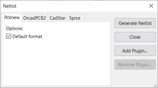
Click Generate netlist and save the .net file in a preferred location.
Generate a PCB
Click Load netlist and select the .net file saved earlier on. Here I encountered some errors. It appears that the J2 header’s footprint was not properly set up. 
Next, click Update PCB and click on the drawing to place the components.
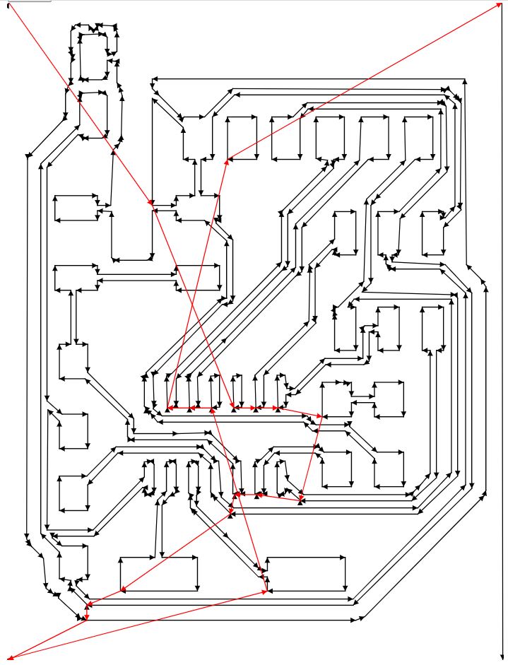
Now I am confused. What are these white lines going all over places? It took me some time to realize that these are the contacts that should be established. Apparently this messy situation is called a rats nest.
Routing the traces
To get out of this messy place, we need to make the traces. There is Autoroute feature but it is meant for large boards. Let’s try to do manual routing for now.
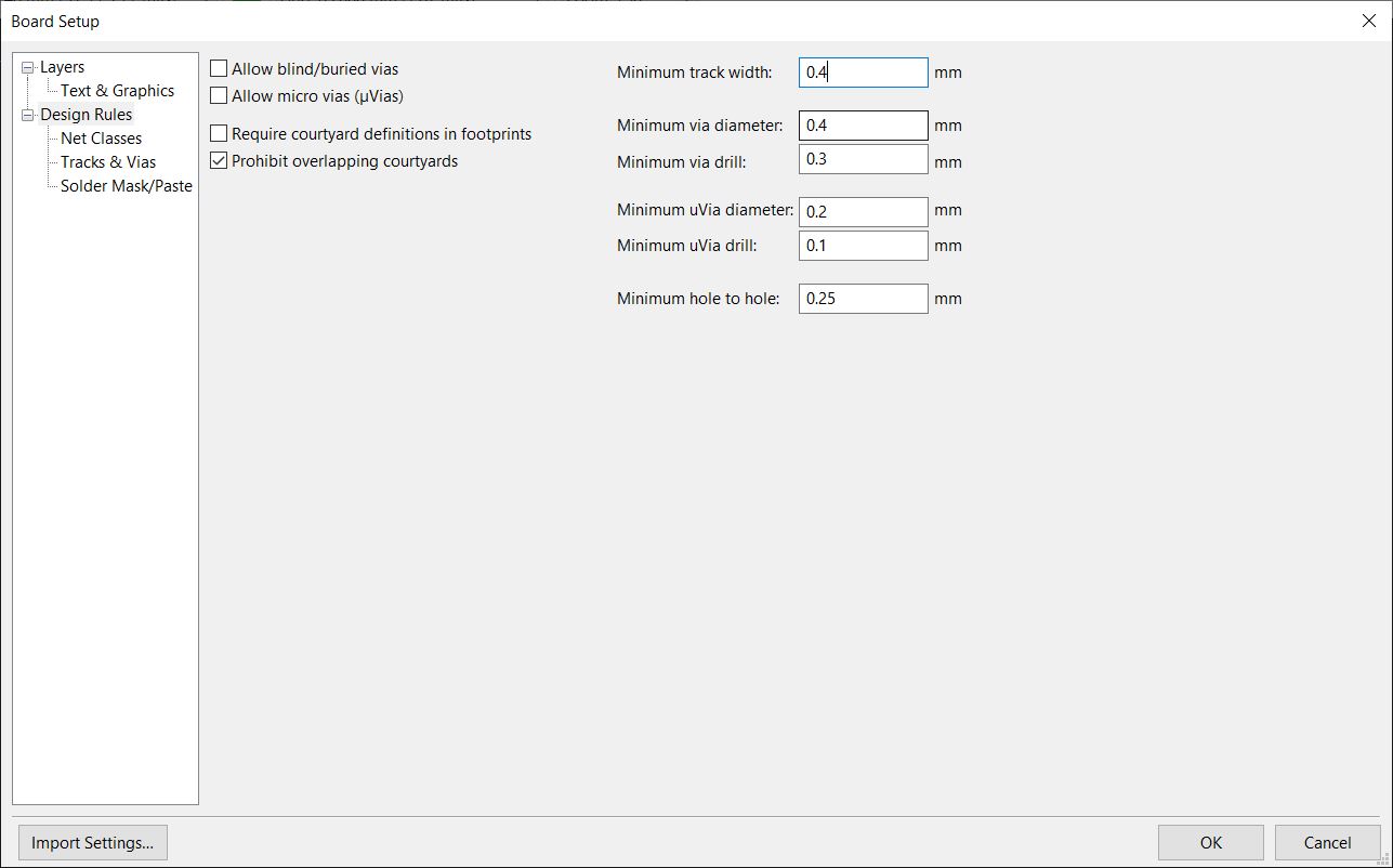
Design rules
In Design Rules tab, I set the set Clearance and Track size to 0.4mm.
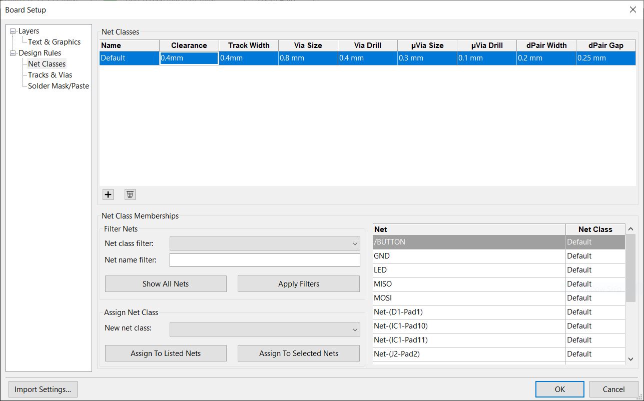
I also set Minimum Track Width to 0.4mm in order to ensure that the traces can actually be milled.
As soon as I pressed OK, an error message appeared.
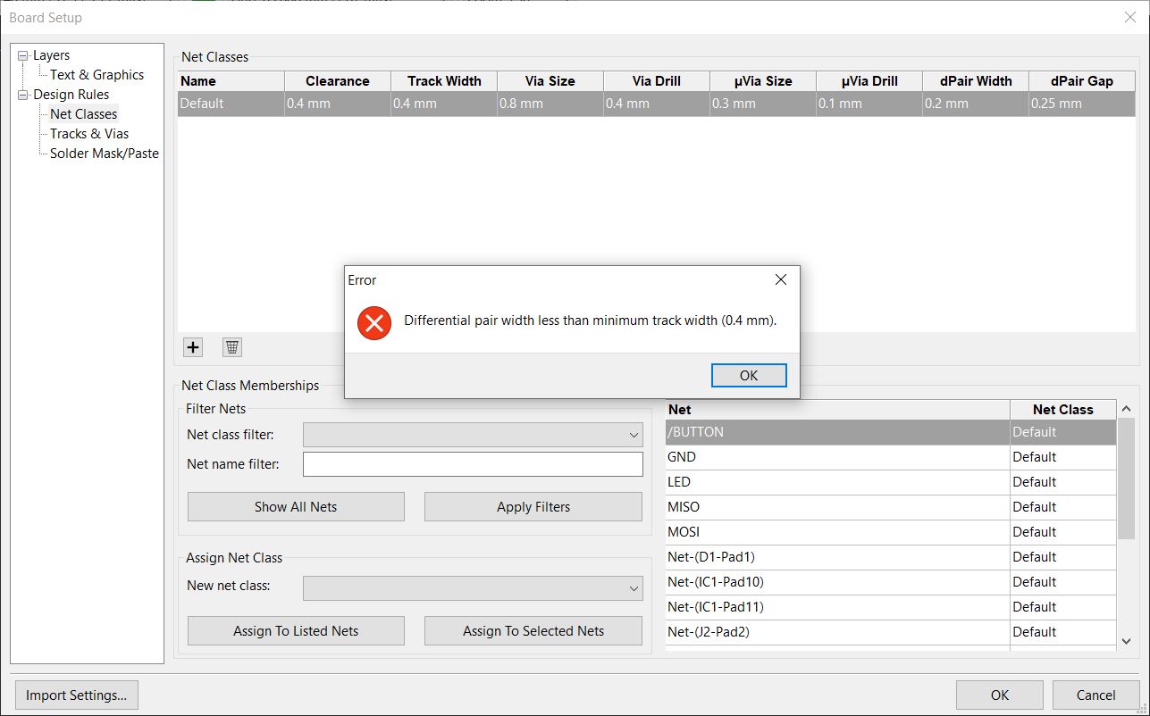
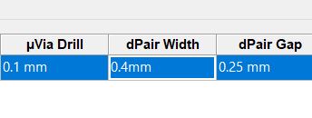
To resolve this, I increased the dPair Width from 0.2mm to 0.4mm and pressed OK.
Eliminate crossing
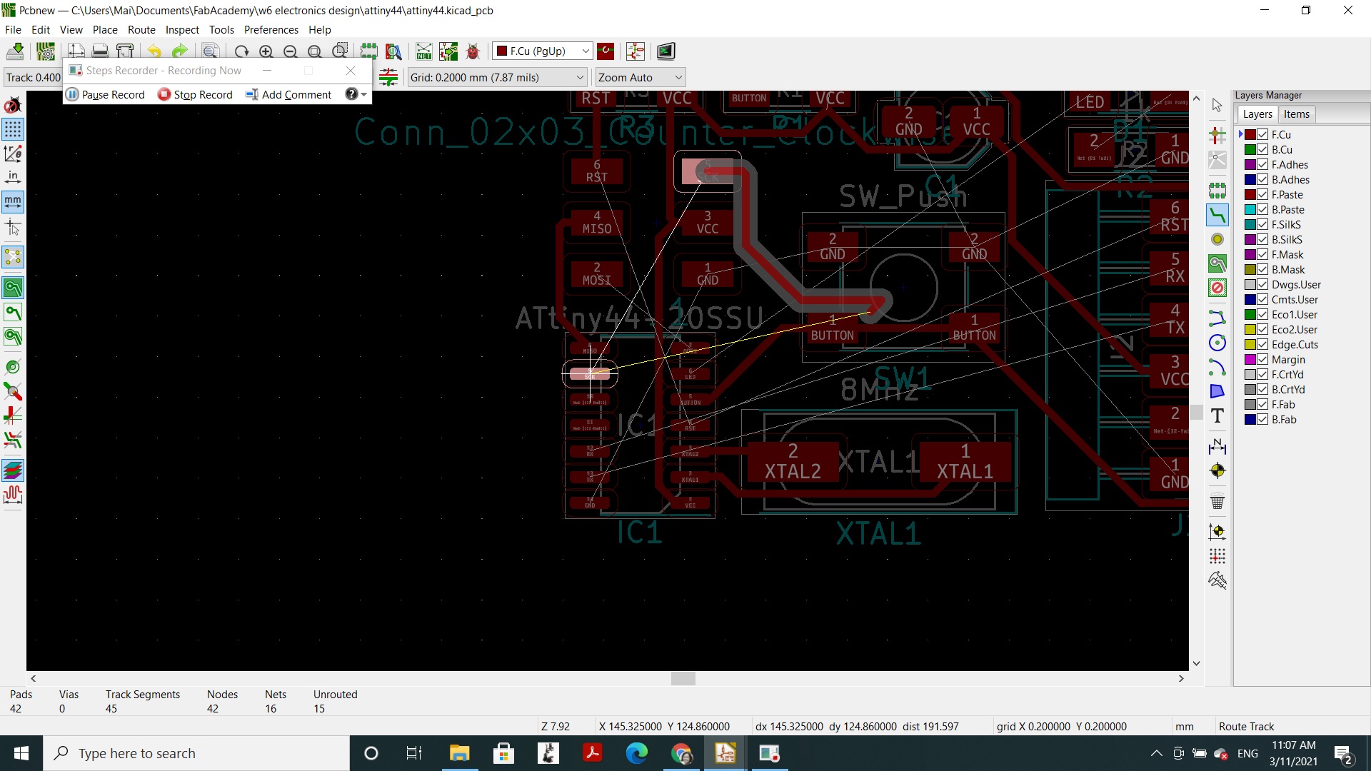
As per Kris from Aalto’s FabLab’s advice, I make the VCC connections first, and leave GND to the last stage. Shortly after, I found myself unable to make a certain trace because there is no way for it to avoid crossing with an existing line. This is where KiCAD will show you a yellow line.
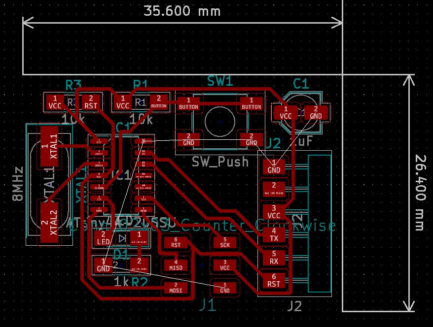
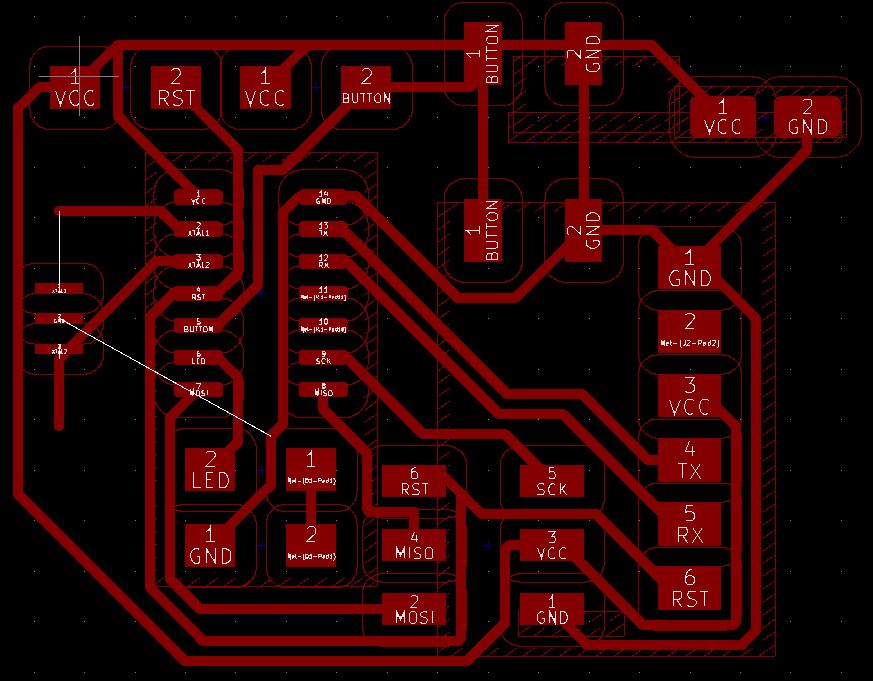
After fiddling with the omponent positions and orientation for a good 3 hours, I arrived here.
Fill copper
Now we will pour a layer of copper on top.
Make sure to deselect Keep out tracks and select Keep out copper pours (and only have the F.Cu layer selected).
In Copper Zone properties, make sure Layer F.Cu is ticked. F.Cu refers to the front side of the PCB, B.Cu back side but it is only relevant to multiple layer boards which is not our case.
In Net, select GND and set the following parameters
- Clearance : 0.8 mm
- Minimum width: 0.4 mm
- Thermal clearance: 0.5 mm
- Thermal spoke width: 0.5 mm
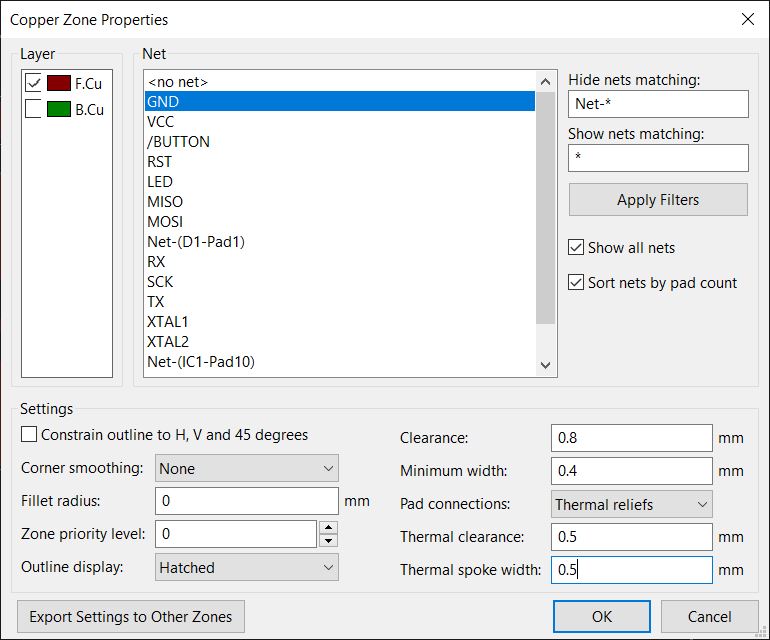
Press OK and you will see that nothing changes.
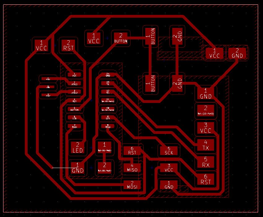
Click Add filled zones and draw where the copper should be filled. My board turned out like this
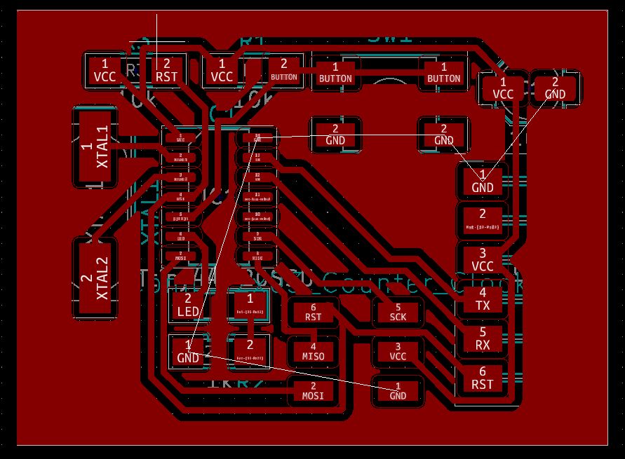
I proceeded to finish up the missing GND connections. To my dismay, the last GND connection cannot be made.
I tried rotating a few things

Hours later, I was still routing. I had no idea that this would take such a long time. Would all the Ai engines do it much faster? Eventually, when I was just about to give up, it worked!!!

At this point, I had an enlightenment. I should route VCC and GND in only one direction, either clockwise or counterclockwise to avoid creating moats that cannot be crossed.
Perform design rules check
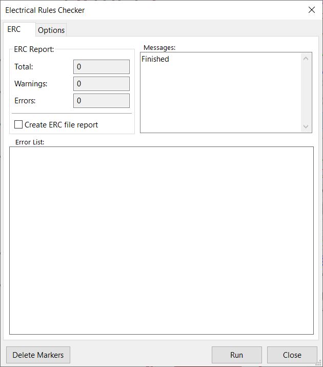
Now, let’s do a final check and see if I pass.
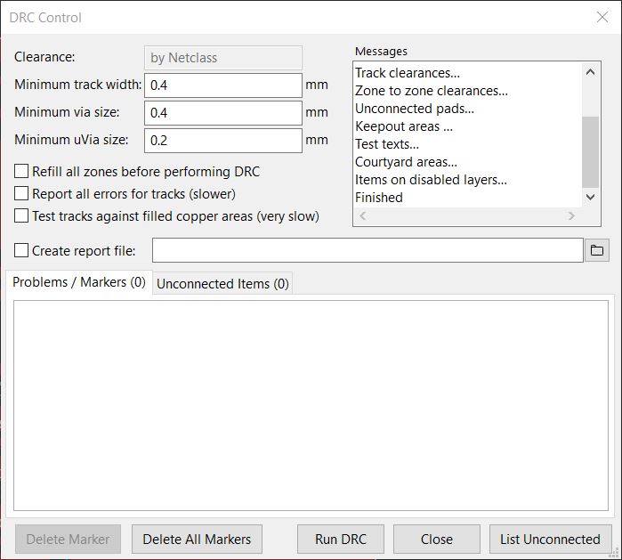
It was such relief when the DRC report came back clean.
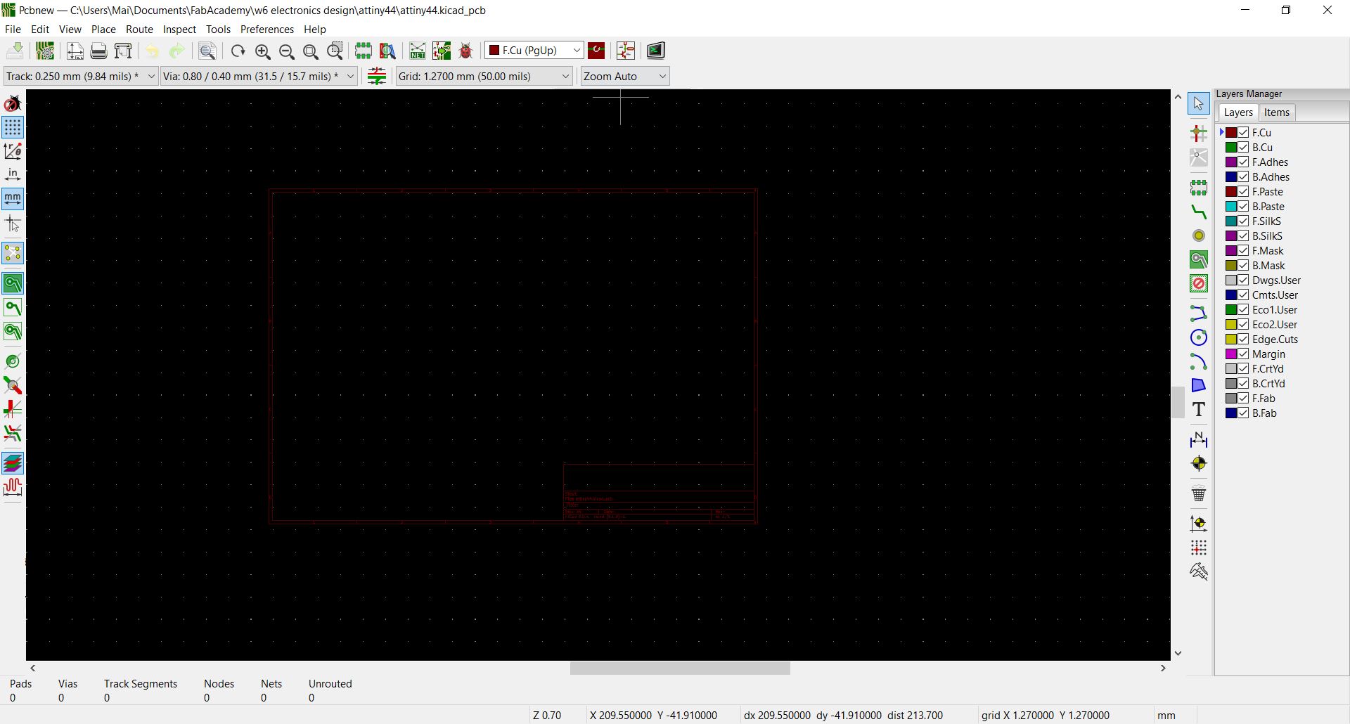
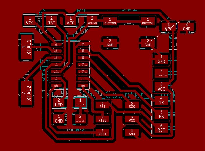
Draw a cutout outline
In Layers pane on the right hand side, I checked only Dwgs.User and used Add graphic lines to draw a rectangle outline.
Add a keepout area
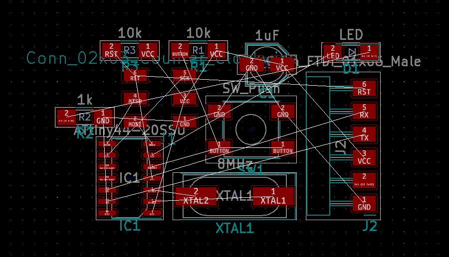
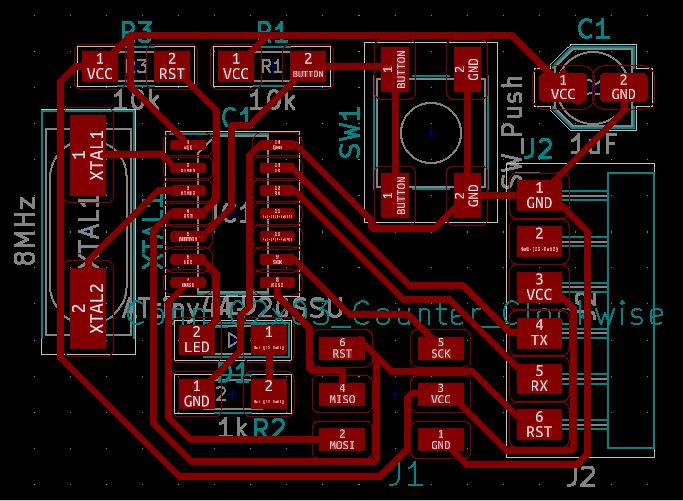
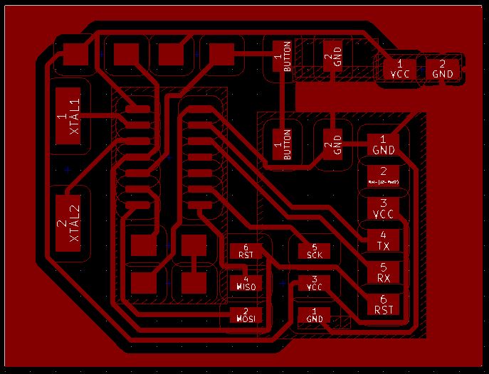
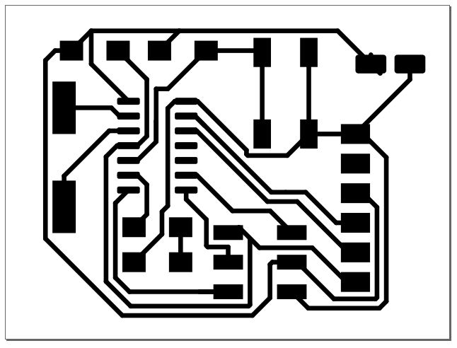
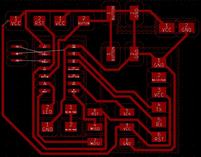
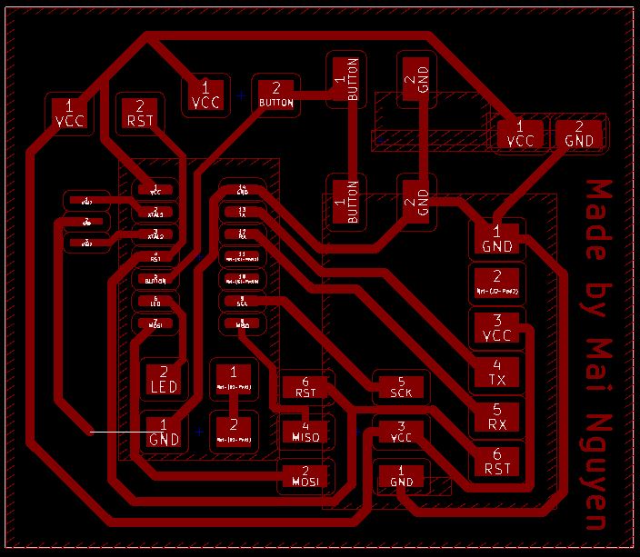
Using Add keepout area button on the right-hand side menu, I drew a rectangle over areas where I want to keep free of copper pour, such as under the chip. I pressed the key B to rebuild the copper pour. Below is a snapshot of my final board.
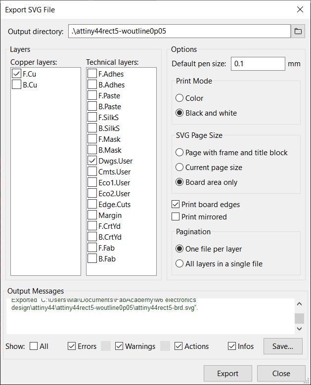
Export SVG
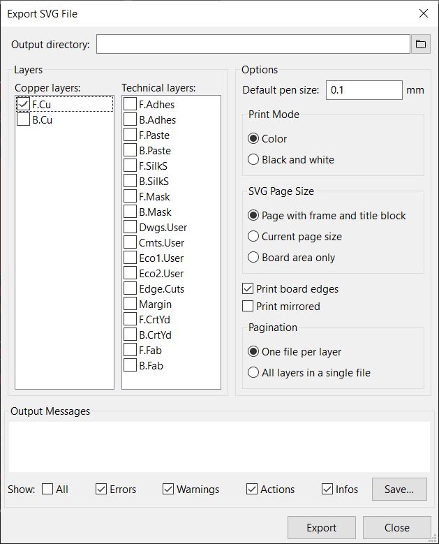
To export the trace and outline into separate files, select F.Cu in Copper layer and Dwgs.User in Technical Layers, then Black and white, Board area only, and One file per layer.
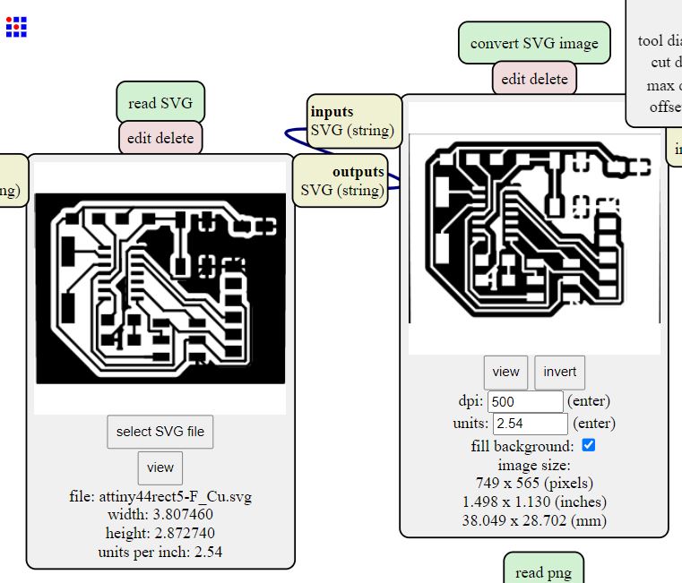
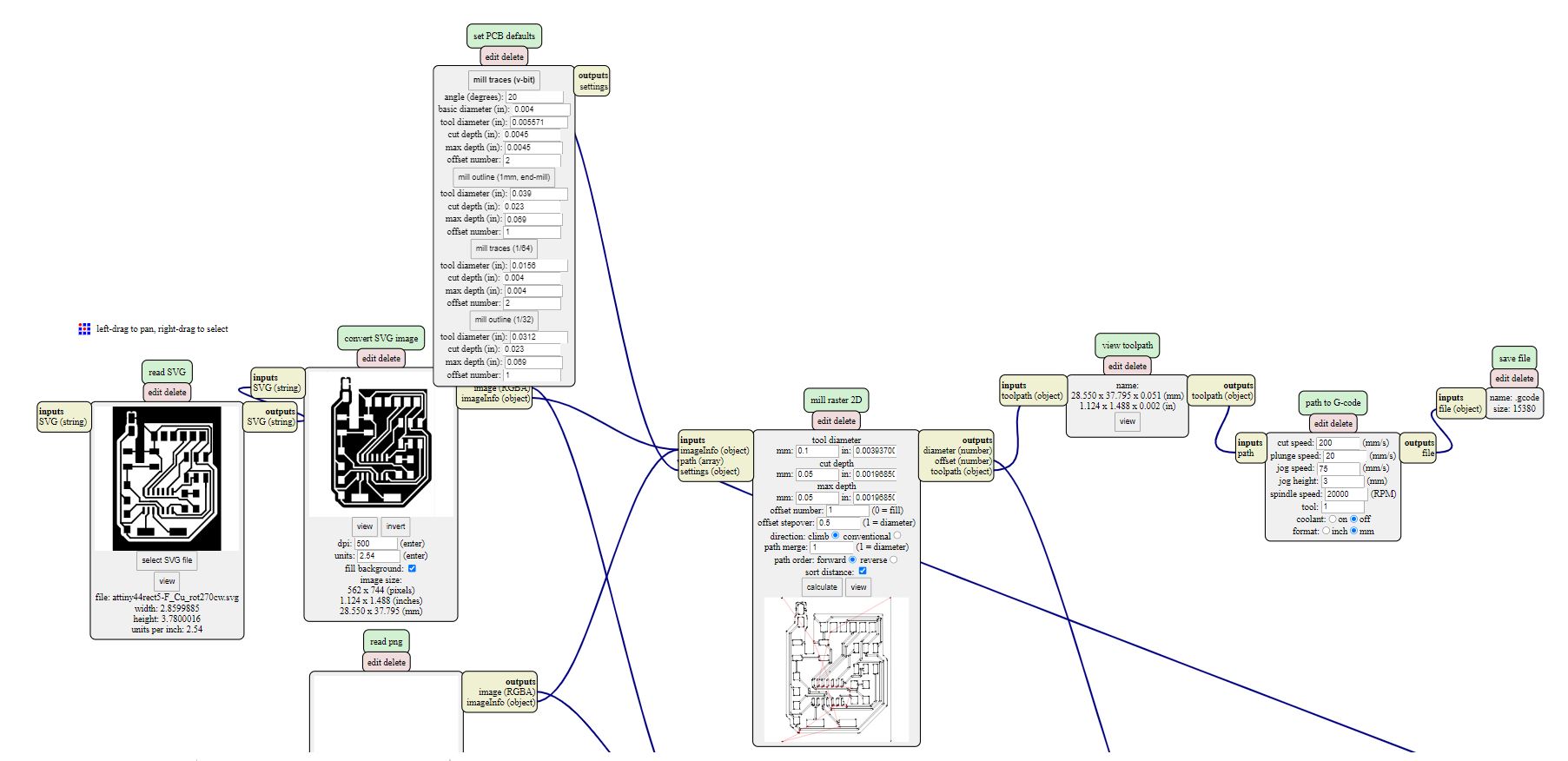
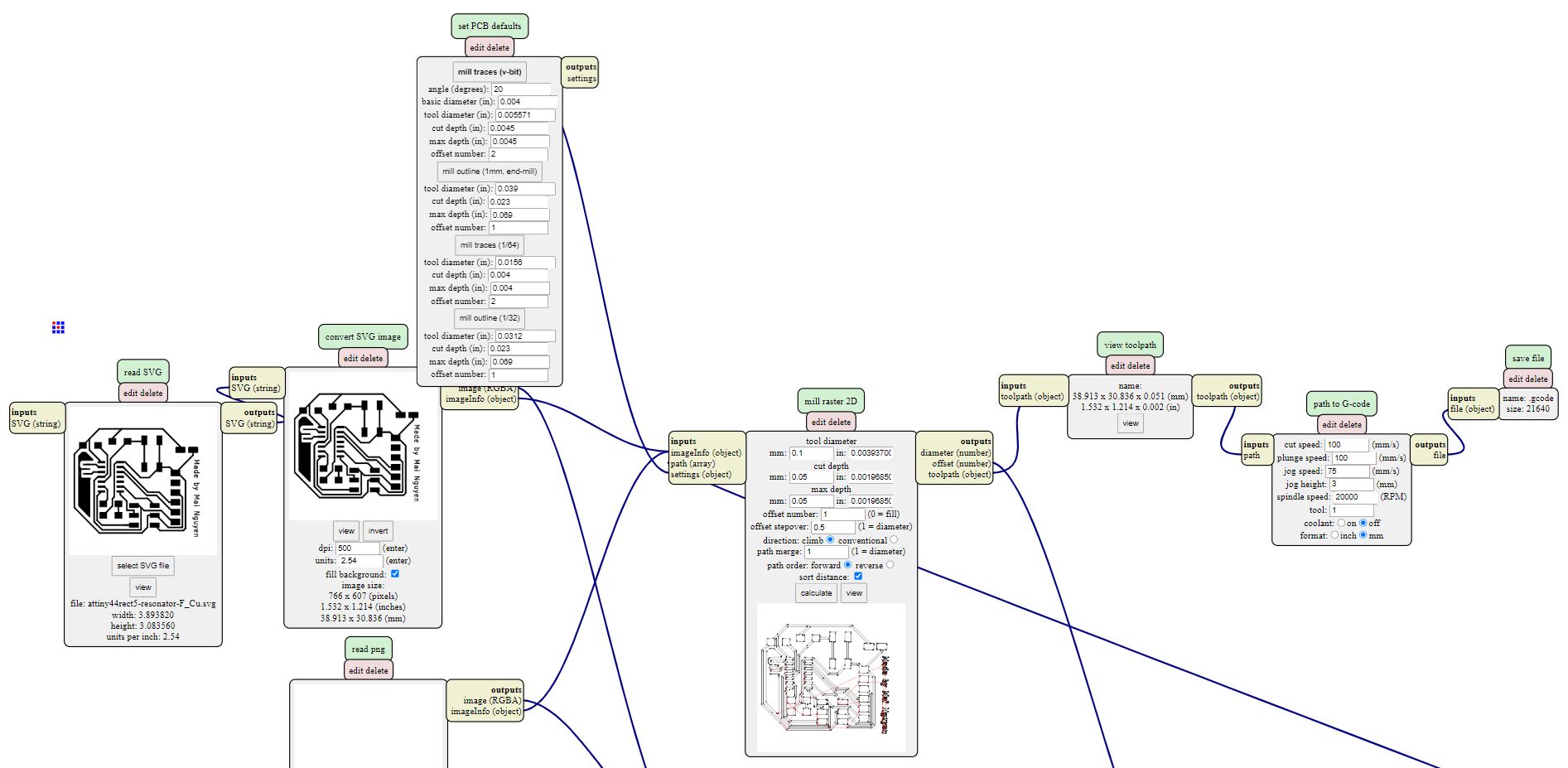
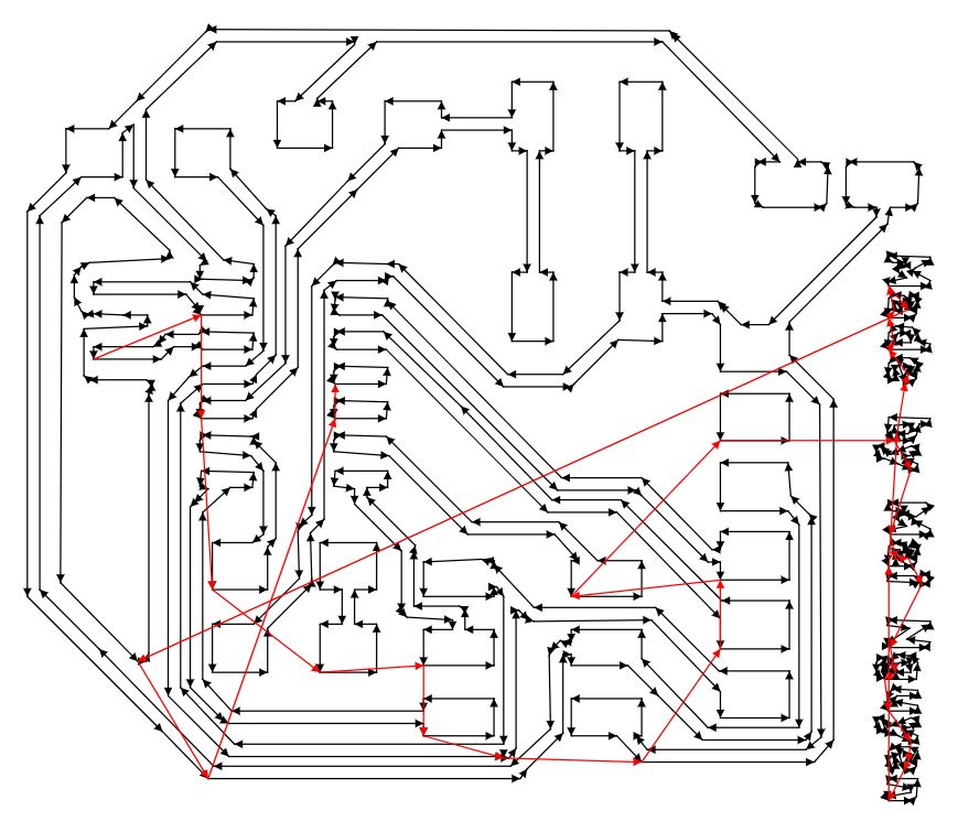
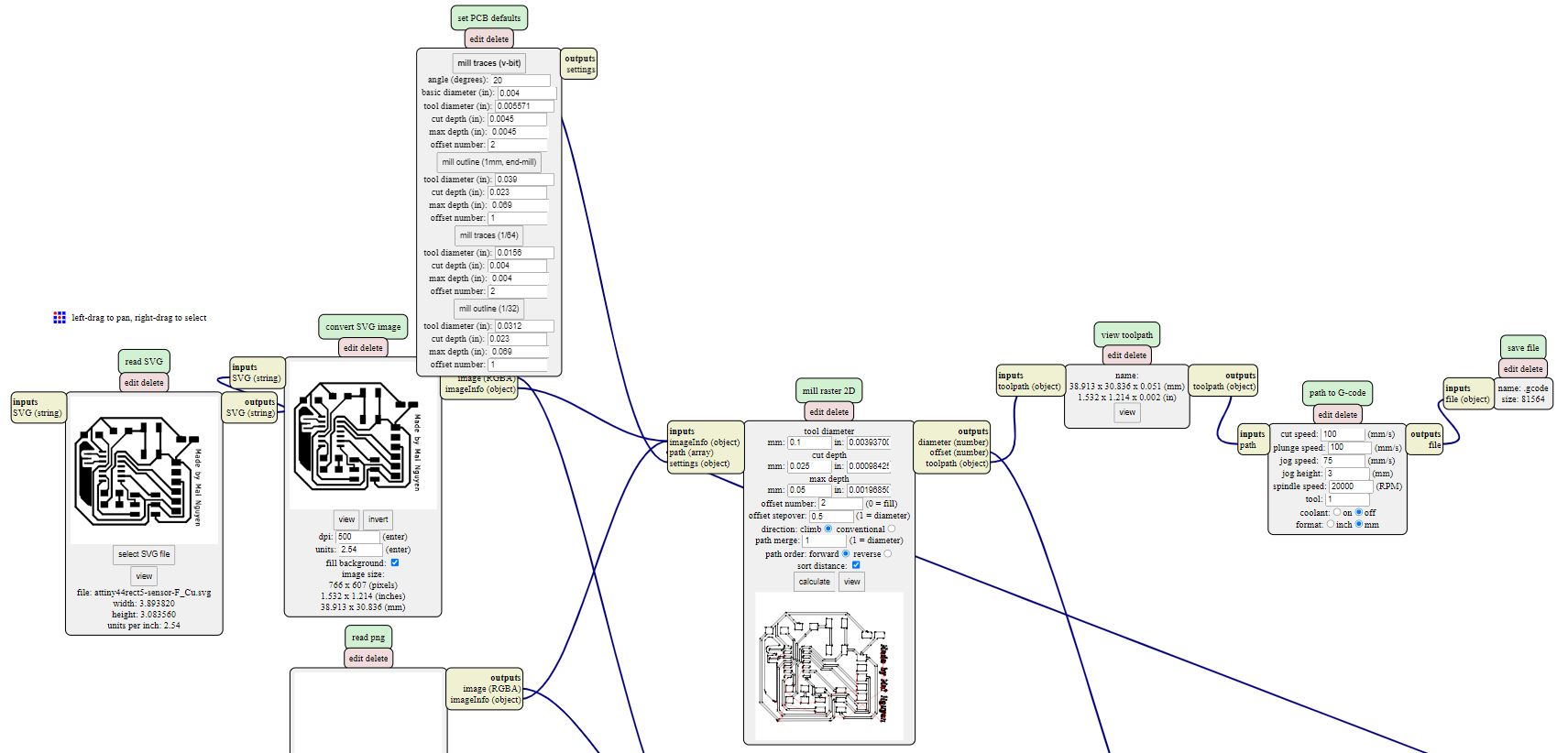
Generate milling paths in MODS
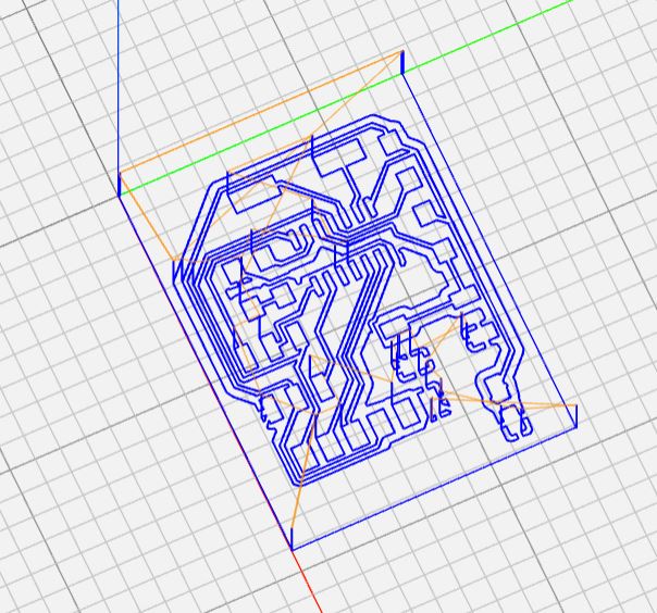
First milling attempt
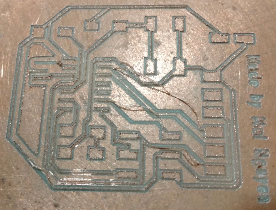
Same as in previous week, I used a 20-degree V-bit with a 0.1mm tip to carve on our home-brew CNC in the lab.
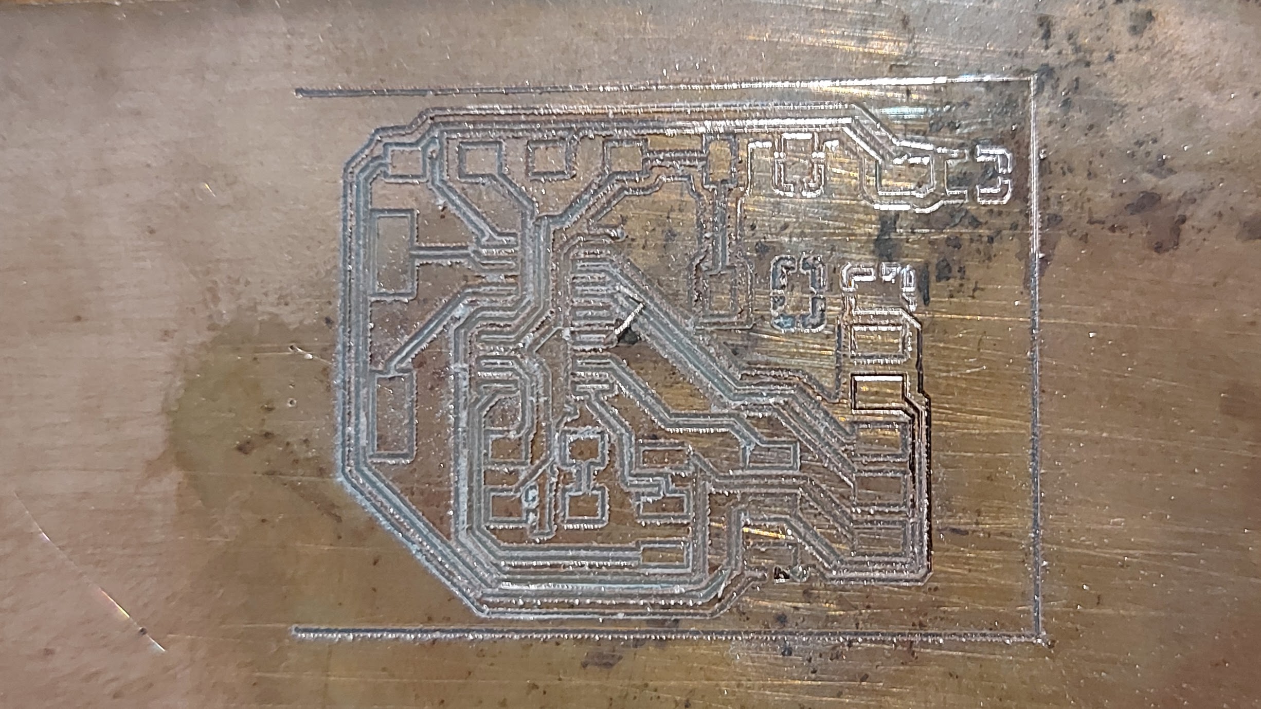
Although I already knew before milling that at 38 x 28cm, the board is very compact and some of the traces are dangerously close to each other, I still wanted to see the limit of our machine. The result confirmed that it is a good idea to space the components further apart in order to give more clearance between the traces. I am also aware that the milling surface is not perfectly flat.
Second, third and forth milling attempts
I asked a friend to let me try milling on his MDX-40A machine. These are the results.

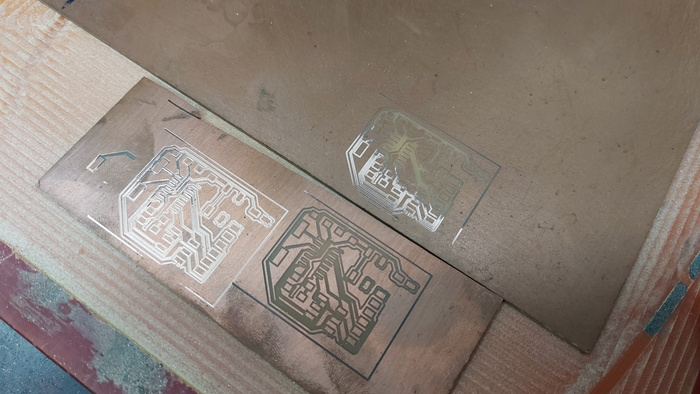
Fifth milling attempt
After 5 milling attempts with a 20-degree V-bit, I still have not got a good PCB to work on. I was totally disappointed. This was the best attempt.
At this point, I think it is necessary to make changes to some tracks to make the milling finish better, for example by avoiding bends and increasing the gaps between tracks.
Making design changes to the PCB
By now, the resonator I ordered - Murata CSTNE12M0G550000R0, had already arrived, so I would need to update the PCB design to replace the crystal with it. My resonator is not the one in Fab Inventory but close enough. According to the datasheet), its size is 3.2 x 1.3mm. However, the Fab inventory’ footprint I plugged in is 3.0x1.1mm.
To be safe, I wanted to make changes on a copy of the current project instead of modifying it directly. As KiCAD does not give an option to save as for the current project, I manually copied all the necessary files (.pro, .sch and .kicad_pcb) and placed them in a new folder. However, when I opened the schematic file, there are strange question marks where the symbol for fab:Conn_FTDI_01x06_Male had been previously. I figured that it is because I had made the fab library as a local and not a global library of the original project.
To fix this, I first added the Fab library to this new project as a global library.
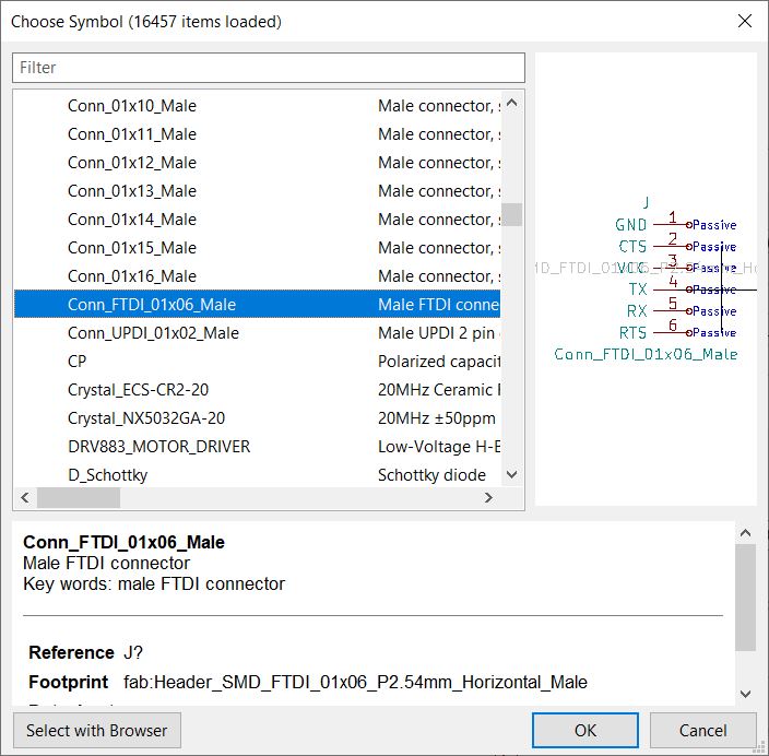
Right clicking on the symbol, then selecting Properties > Edit properties, I opened the Symbol properties window:
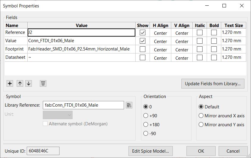
Scrolling down to Library reference field, I clicked on the books icon next to “fab:Conn_FTDI_01x06_Male”. This opens the Choose symbols window where I clicked on Fab, selected ‘Conn_FTDI_01x06_Male’ and clicked OK. I press OK once more to close the Symbol properties window. And that’s how I got the symbol back to what it used to be.
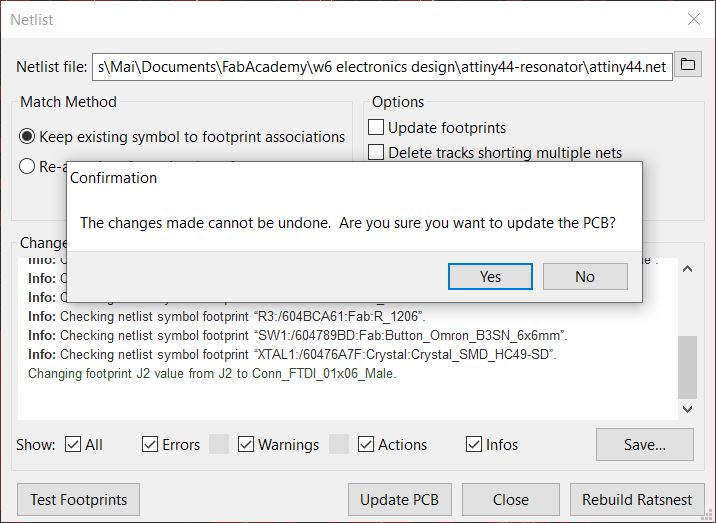
Next I opened the PCB file and clicked on the ‘Load Netlist’ button. I pressed Yes to confirm and subsequently pressed ‘Update PCB’. All went well.
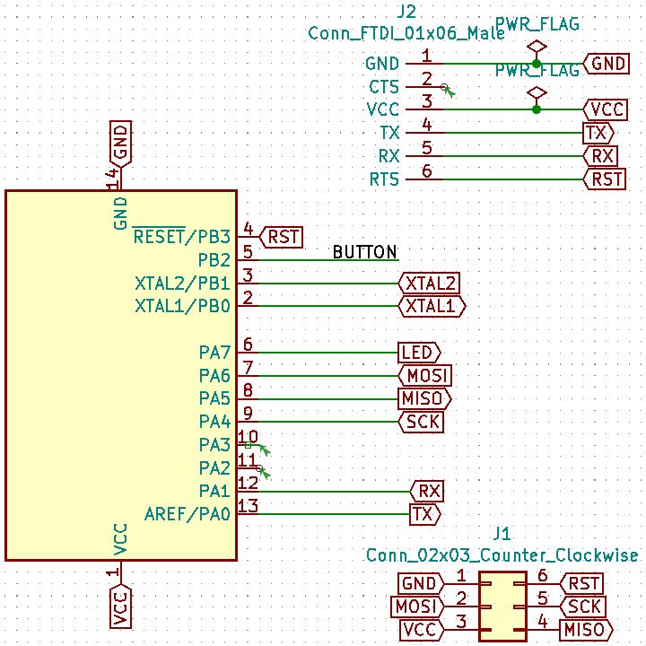
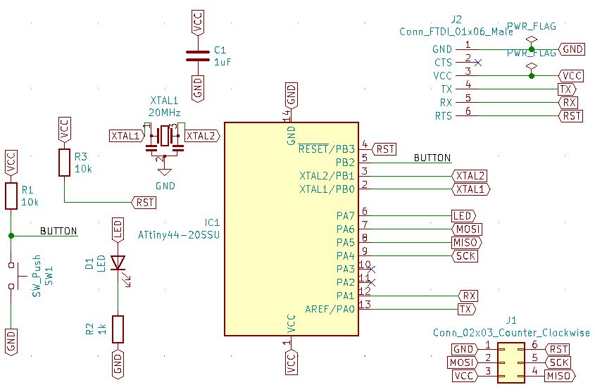
I proceedded to replace the capacitor symbol with a resonator, and perform electrical rules check. Below is a shot of my schematic following the changes.
Next, I proceeded to ‘Generate Netlist’ and ‘Run Pcbnew’ hoping that the resonator footprint would neatly appear in the PCB layout. That did not work. Neither did clicking on ‘Update PCB from schematic’ help. Instead, I had to manually ‘Load netlist’ and point to the newly generated netlist, while specifying ‘Re-associate footprints by reference’ for the match method. Additionally, ‘Update footprints’ and ‘Delete extra footprints’ are also selected.
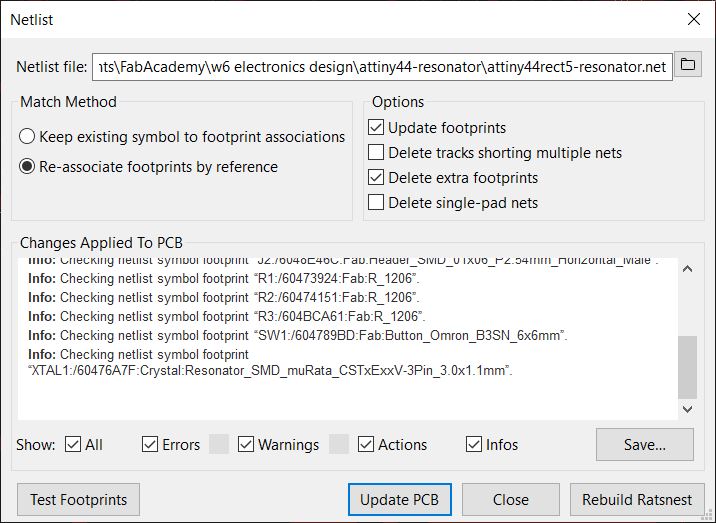
Gleefully, upon my clicking ‘Update PCB’, the resonator footprint finally came into picture.
Eventually, I sought help from Rico who pointed out that I should increase go to Board Setup and change the Clearance value from 0.8 to 0.4. It felt like magic when the traces between the resonator and the chip can be made instantly.
To enlarge the rectangle cutout shape, I checked only Dwgs.User in the Layers pane on the right hand side and used Add graphic lines to re-draw the rectangle.

The last issue is how to route to GND connection from the resonator without jumping over the existing traces. It seems like a mind-boggling task which I do not have the hours to put in. My temporary fix is to jump a wire from here to the ground connection for the LED.
Sixth milling attempt
My MODS settings this time can be found below.
Widening tracks to 0.5mm
To make the tracks harder to peel off, I tried changing the track width from 0.4mm to 0.6mm but 0.6m track cannot pass in some areas. The biggest possible is 0.5mm, but even that cannot be applied to all traces under the chip or inbetween two pads on a connector. A combination of 0.5mm and 0.4mm work best. Track width can be changed by editing pre-defined tracks and adding a custom width.
My MODS setting for this attempt:

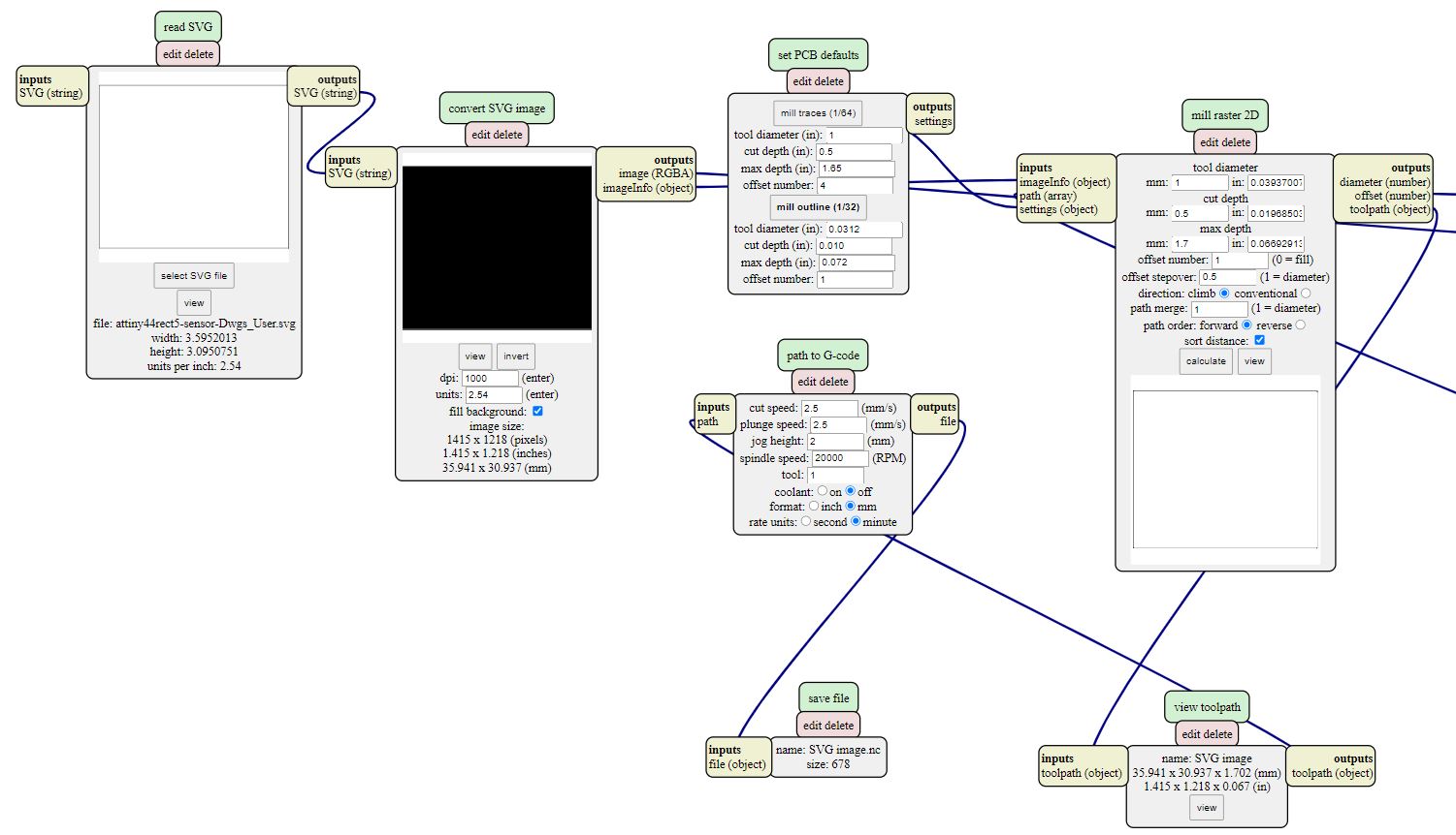
Cutting out the PCB
For this cutting job, I changed the milling bit to a 1mm corn type.

I opened MODS in my browser and clicked on Programs > Open server program > G-code > mill 2D svg.

Using a knife, I lifted up the board easily.
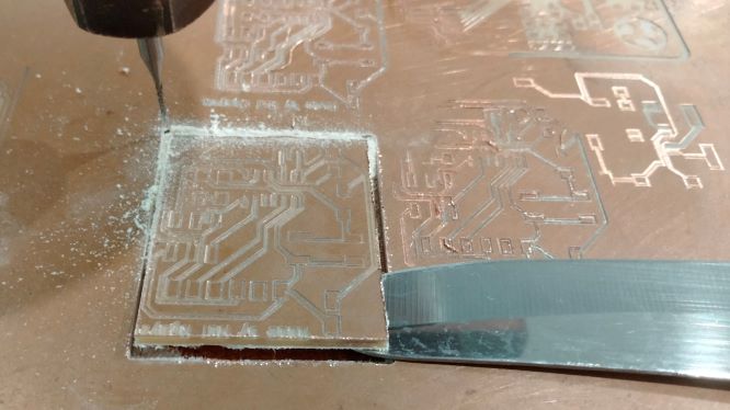
and the result
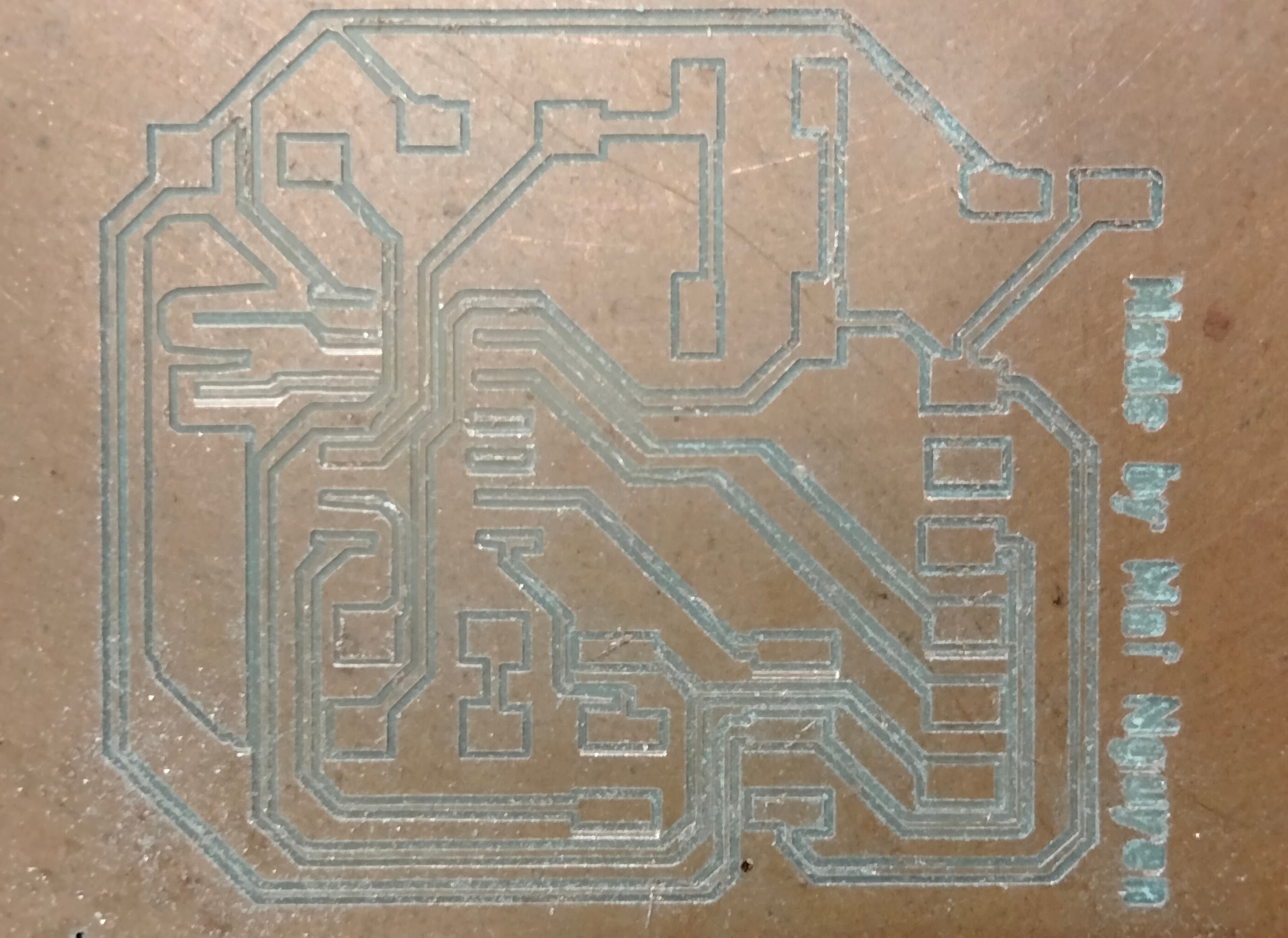
Some of the traces are incredibly thin and fragile. It is best to run a continuity test with a multimeter before proceeding to solder.
Considering that the TX trace was broken and the RX one can disintegrate anytime, I wanted to re-mill another board. Too bad I was short on time and I ended up patching the traces for the sake of completing the exercise, forgoing the aesthetics of the circuitry. My circuit board might be ugly as heck, but it works, and I am so happy and proud!
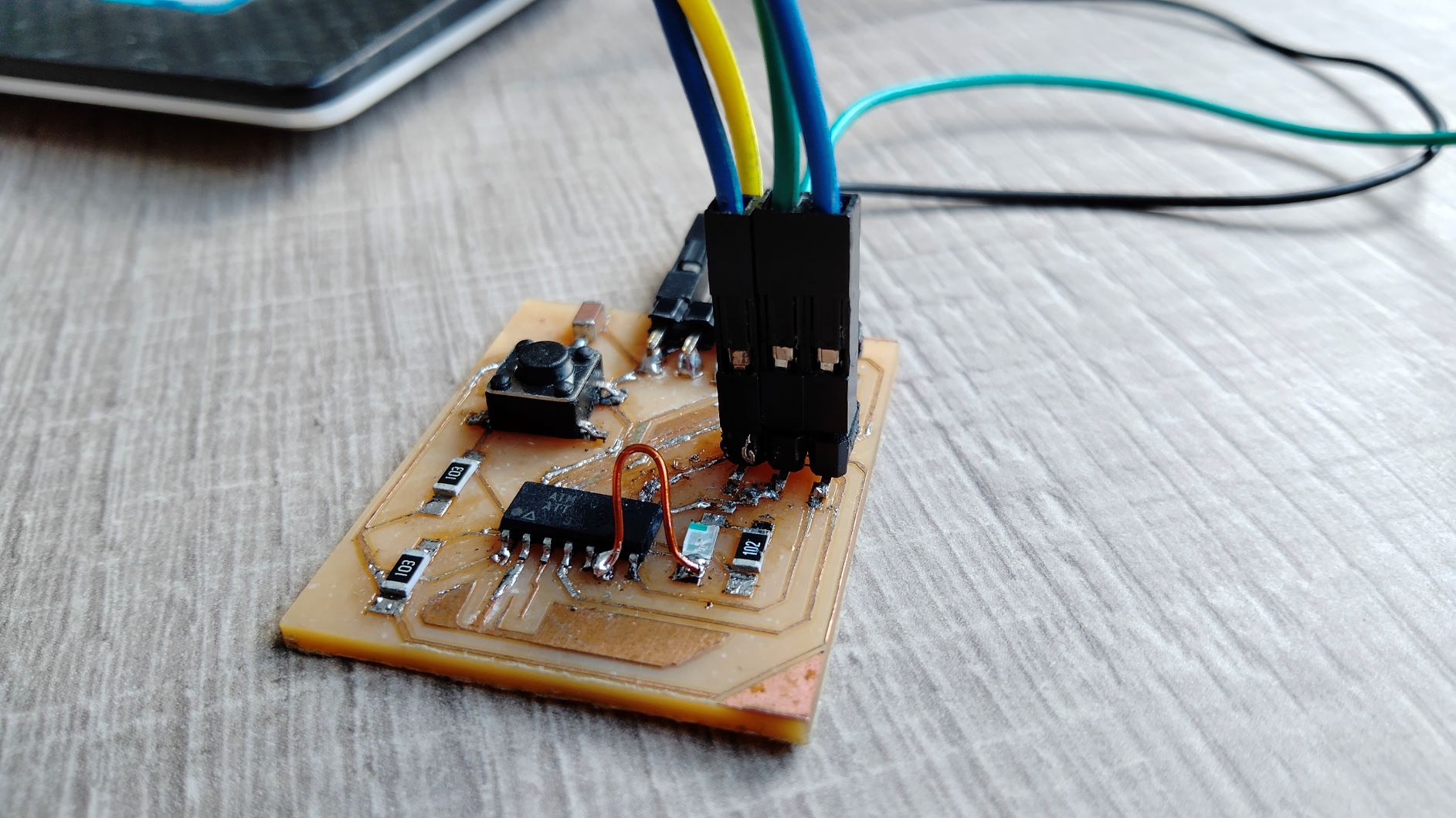
Stuffing the PCB
I stuffed the PCB in the following order: MCU, SPI header, LED, 1k resistor, 10k resistors, capacitor, button, 01x06 header. Before soldering each component, I applied flux on the soldering pads. It helps the solder to flow.
This is my achievement
Unexpectedly, the connection between the LED and the ATtiny’s pin 6 failed upon checking with a multimeter. I had made sure the trace worked before soldering the MCU so this surprised me. To save the day, I quickly soldered a little bridge with a copper wire.
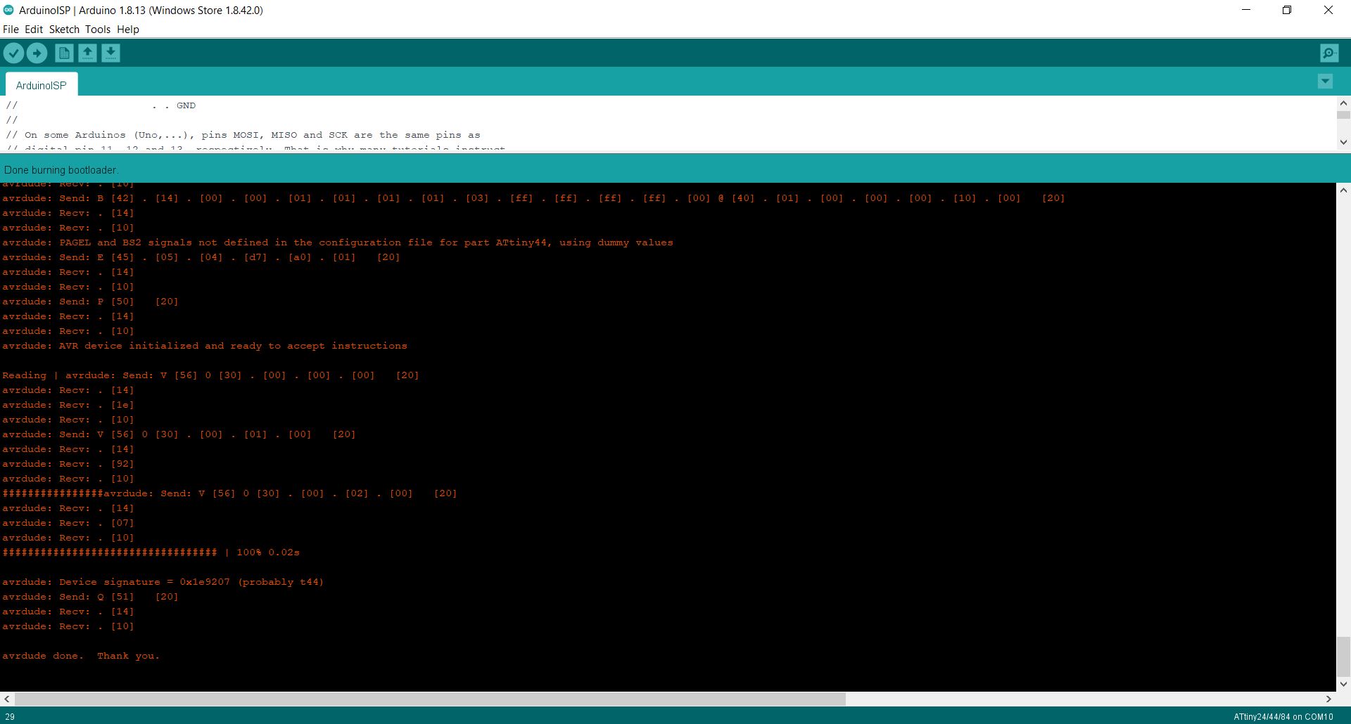
Burning the bootloader
Two weeks ago, I was not able to make a FabISP with our CNC machine. Now, I need an in-system programmer(ISP) in order to burn the bootloader for my new board. Without a dedicated ISP on hand, I turned to the almighty Arduino Uno. With some wiring and a bit of programming, it can act as a programmer.
Following this tutorial by David Mellis, I learnt the steps to set up my ISP circuit.
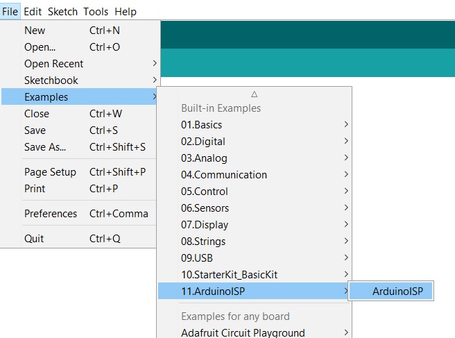
First up, in Arduino IDE, I loaded a sketch called ArduinoISP by going to File > Examples > 11.ArduinoISP and selected ArduinoISP. This opened a new sketch.
I selected the following in Tools setting
- Processor: Arduino Uno
- Programmer: AVR mkll
I pressed Upload to send the ArduinoISPU sketch to the Uno. It was successful.
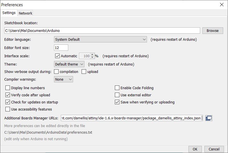
I clicked on Preferences and in the field next to Additional Board Manager URLs, I pasted the following link and pressed OK. https://raw.githubusercontent.com/damellis/attiny/ide-1.6.x-boards-manager/package_damellis_attiny_index.json
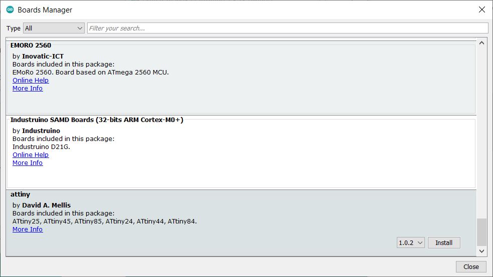
In Tools > Board > Board Manager…, I scrolled all the way down until I found Attiny and clicked Install.
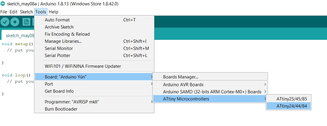
Going back to Board, I clicked on ATtiny microcontrollers and selected the ATtiny24/44/84 family.
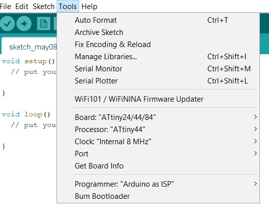
The rest of the Tools setting is as follows
- Processor: ATtiny44
- Clock: Internal 8MHz
- Programmer: Arduino as ISP
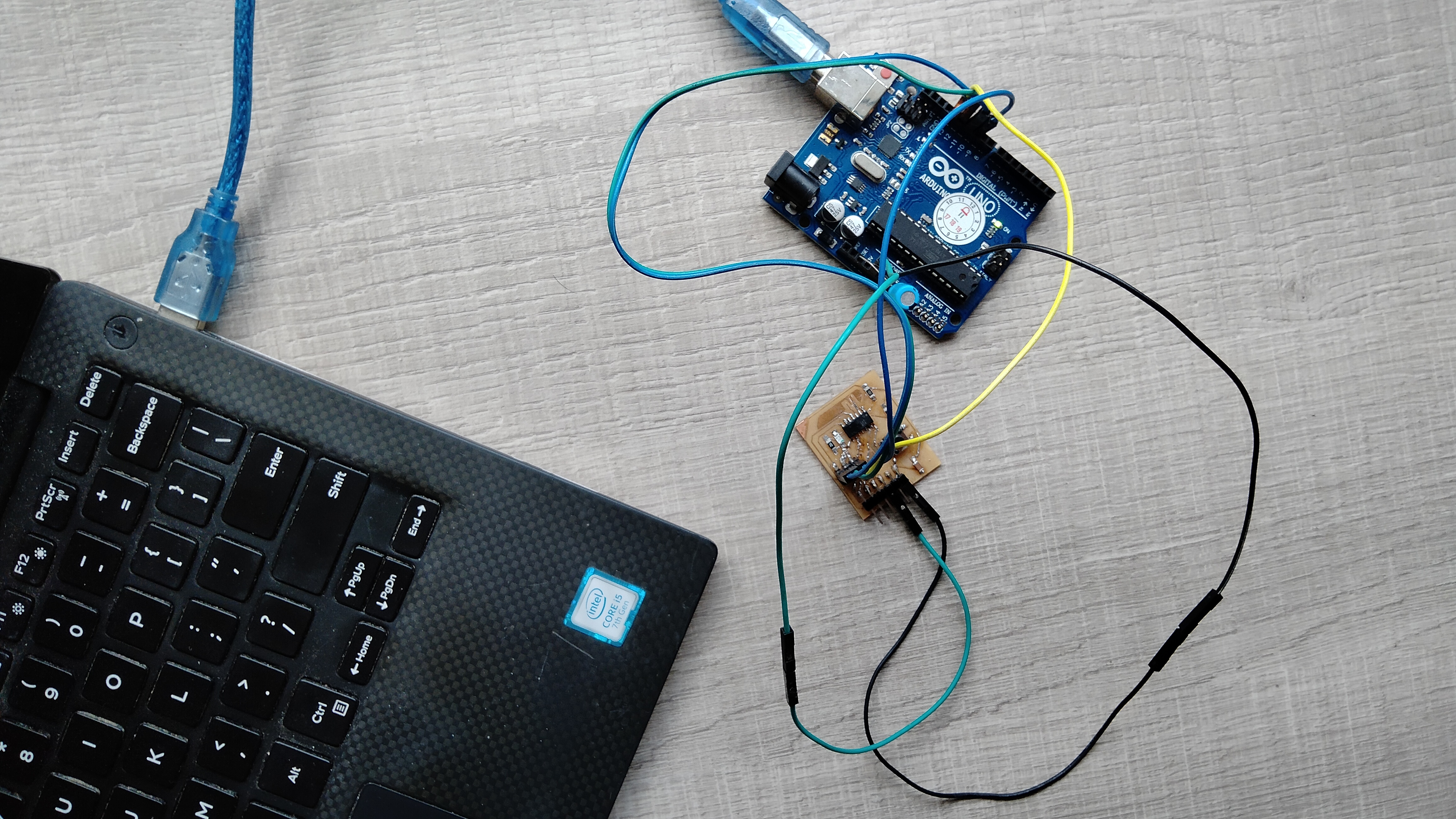
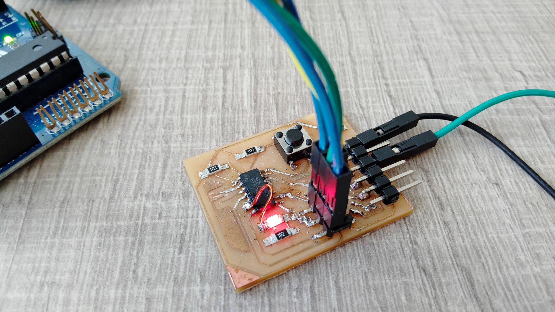
Before we could turn Arduino Uno into a programmer, there is some wiring to do:
- wire the SCK, MISO, MOSI and RST pins on my board to the Arduino Uno’s pin 13, 12, 11 and 10 respectively.
- add a 10uF capacitor between the RST and GND pins on Arduino Uno (the negative side of the capacitor going to GND). This will prevent the Uno from resetting itself which starts the bootloader.
However, since I do not a 10uF on hand, I used a 33uF capacitor instead. Below is a shot of the wiring.
Now all is ready to buuuurn (the bootloader, of course). When done, the IDE will tell you Done burning bootloader.
Programming
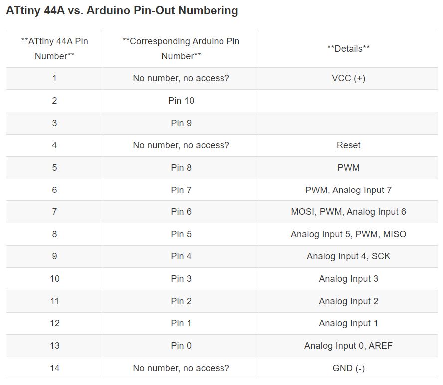
I wrote a tiny sketch to blink the LED. To know which pin I should connect to, I referred to this handy pinout mapping from a Fab Academy tutorial.
The sketch was successfully uploaded, and the LED blinked as expected.
Here is my code.
/*
 * Blink LED
 */

int ledPin = 7;                // choose the pin for the LED

void setup() {

  pinMode(ledPin, OUTPUT);     // declare led pin as input

}

void loop(){

  digitalWrite(ledPin, HIGH);
  delay(500);
  digitalWrite(ledPin, LOW);
  delay(500);

}
A stretch goal for PCB design
As a long-time fan of artistic PCBs, I was thinking of a “banh mi” or “Vietnamese baguette” shape for my PCB. It is more or less like a pointed oval. I made a quick drawing in Inkscape like this
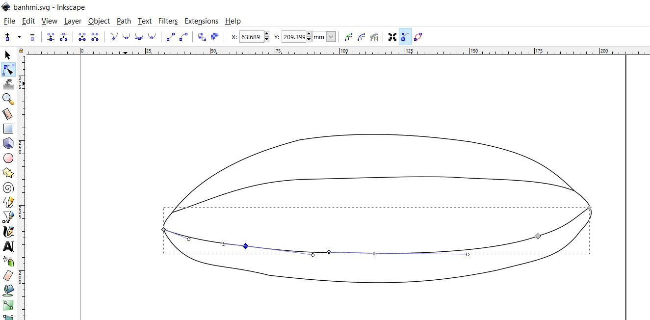
As a result, I need to re-arrange the components in the middle and along the length of the baguette.
Soon I realized that it is not possible to import a custom vector into KiCAD itself so I started searching and came across a means to add an artistic flair to a PCB - Svg2Shenzen Plug-in.
Svg2Shenzen Plug-in for making artistic PCBs
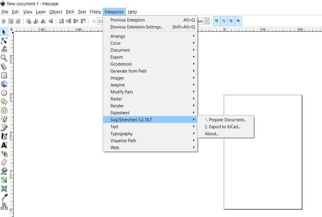
For those wanting to add an artistic flair to their PCBs, Svg2Shenzen is an interesting Inkscape extension for exporting drawings into a KiCad PCB.
I downloaded version 0.2.18.7 and copied the unzipped content to Inkscape extensions folder.
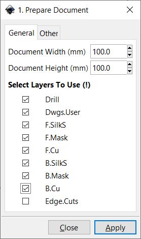
When you click on Prepare Document, you can select layers to import from KiCAD. I only ticked F.Cu and Dwgs.User.
Once applied however, an error came up. The end of the error message mentioned an Attribute error.
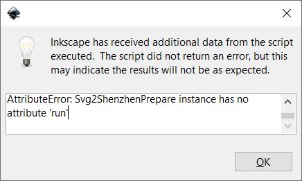
According to this advice, I should be using Inkscape 1.0. I am currently on Inkscape 0.92.
Unfortunately, I did not have enough time to investigate further, so I just left it at that. By the way, another blogger had no issue with version 0.2.15. If interested, you can check that out. ‘
Learning the hard way
To go from a PCB user to a PCB designer adds new perspectives to my knowledge. While I am not at all unfamiliar with PCBs, I did not know that manual routing even for a board as simple as mine is almost a head-banging experience.
I also did not expect PCB milling to be so delicate. It took much more time than I had imagined to get things right, especially with my v-bit setup. The surface needs to be perfectly flat and the tip needs to be in very good condition as well.
1. Píns not connected due to wires not touching header holes
When you draw a wire, do make sure that the wires go all the way to the header hole. Otherwise, many warnings of pin not connected will come up when you run an Electrical Rules Check.
Like this is NOT OK
OK
2. DO use the fab library
3. Adding footprints takes time if you use components outside fab inventory
Fun facts
Resonator vs Crystal oscillator
Crystal oscillator has low ESD (Electrostatic Discharge) tolerance while the ceramic resonator has a high ESD tolerance. Oscillators are more sensitive than the resonators, the sensitivity can be compared in terms of radiation. Quartz has a 0.001% frequency tolerance, while PZT has a 0.5% tolerance.
What is FTDI?
For those interested, FTDI stands for Future Technology Devices International , a company making chips for USB communication. The FTDI cable is a USB to Serial (TTL level) converter which allows for a simple way to connect TTL interface devices to USB. … The other side of the cable is terminated with a 0.1” pitch, 6-pin connector with the following pinout: RTS, RX, TX, 5V, CTS, GND (RTS is the green cable and GND is black).
Useful links
- Electronics Design with KiCAD
- CREATE NETS AND LABELS
- KiCAD libraries for component footprints
- Tutorial by High-low tech on using Arduino as ATtiny programmer
- Tool for making artistic PCBs