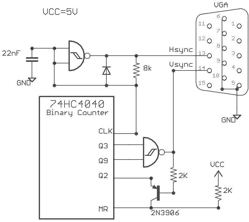
18. Project Development¶
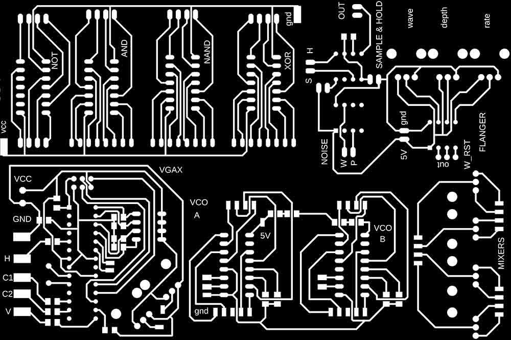
Final Electronics Files + Milling Lines¶
The board:
FULL_BOARD_REV3_8 CORRECTIONS.brd
The schematic:
FULL_BOARD_REV3_8 CORRECTIONS.sch
The Eagle generated BOM:
FULL_BOARD_REV3_8 CORRECTIONS.txt
The milling file (top and bottom):
The knob 3D model in Rhino and STL formats:
Questions + Answers¶
Please refer to week 16 for the answers to the following questions:
What does it do? Who’s done what beforehand? What did you design? What materials and components were used? Where did they come from? How much did they cost? What parts and systems were made? What processes were used?
For these answers look below:
What questions were answered?¶
Circuits designed for audio synthesis can indeed be used for video synthesis but they need to be run faster. Depending on the screen resolution this can be a challenge for logic chips. The HTC family works to 40MHz it seems, and that is why I chose to work with 600x800 pixels because the pixel frequency is 40MHz.
What worked? What didn’t?¶
What didn’t work:
- My CNC milled enclosure wasn’t perfectly aligned with the circuit below (because it was an SMD circuit and didn’t use drilled holes to perfectly align components) making it difficult to plug in jumpers and install the knobs.
- My knobs were too brittle and snapped off to easily.
What did work:
- One can spend hours experimenting and making funky signals !
How was it evaluated?¶
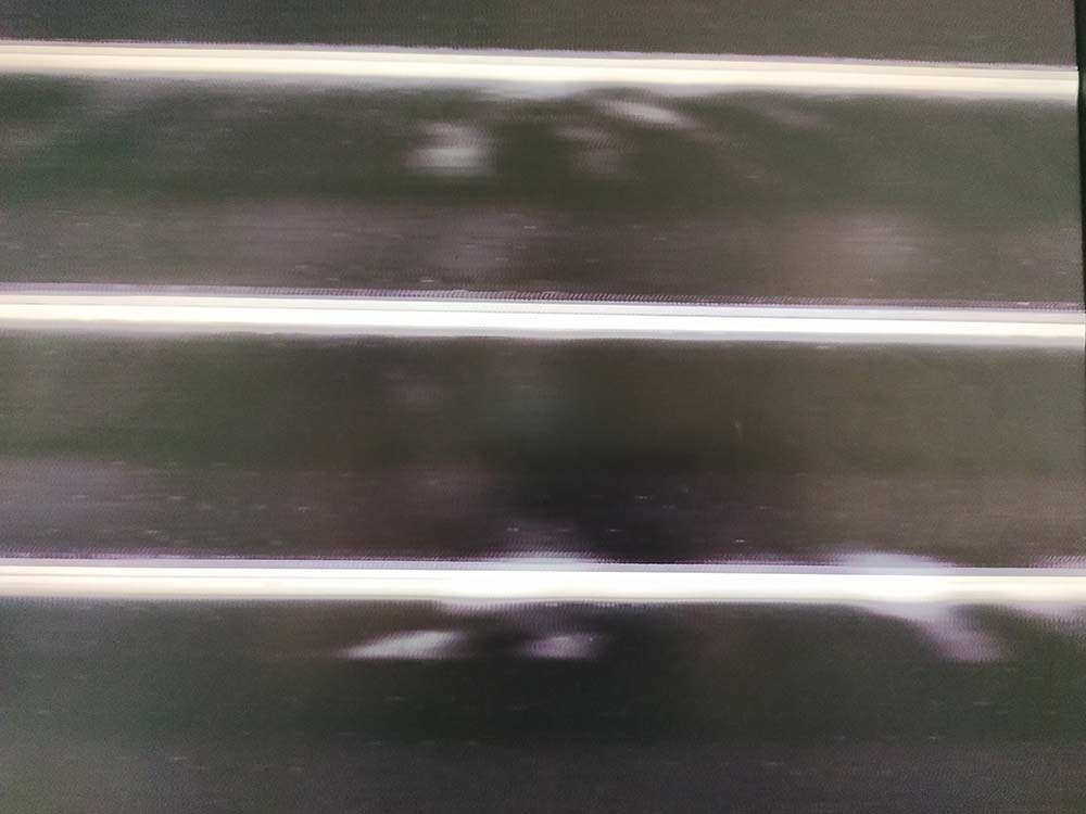
I am still evaluating the variety of output that this device can produce. So far I am discovering that certain effects (horizontal lines) are easier than others to produce (vertical lines, for instance).
What are the implications?¶
After spending the time to really evaluate the full scope of visual effects I can produce I would like to redesign this once more. At that point, and once I have moved further from pre-existing work on cmos synthesis, I could potentially have a video synth product that might interest someone.
Experiments¶
What follows is a diary of me developing the final project:
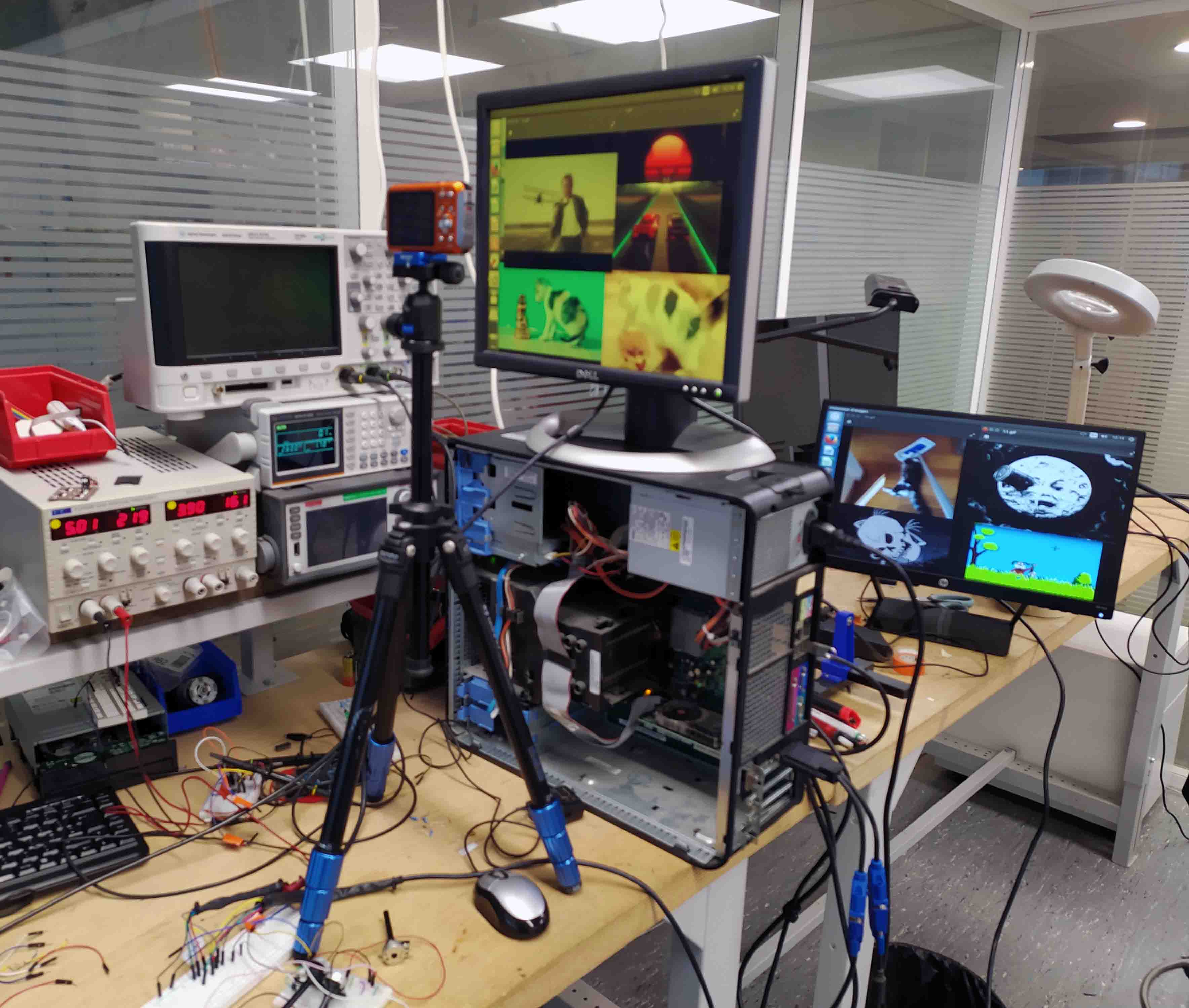
Here is my test set up at the moment:
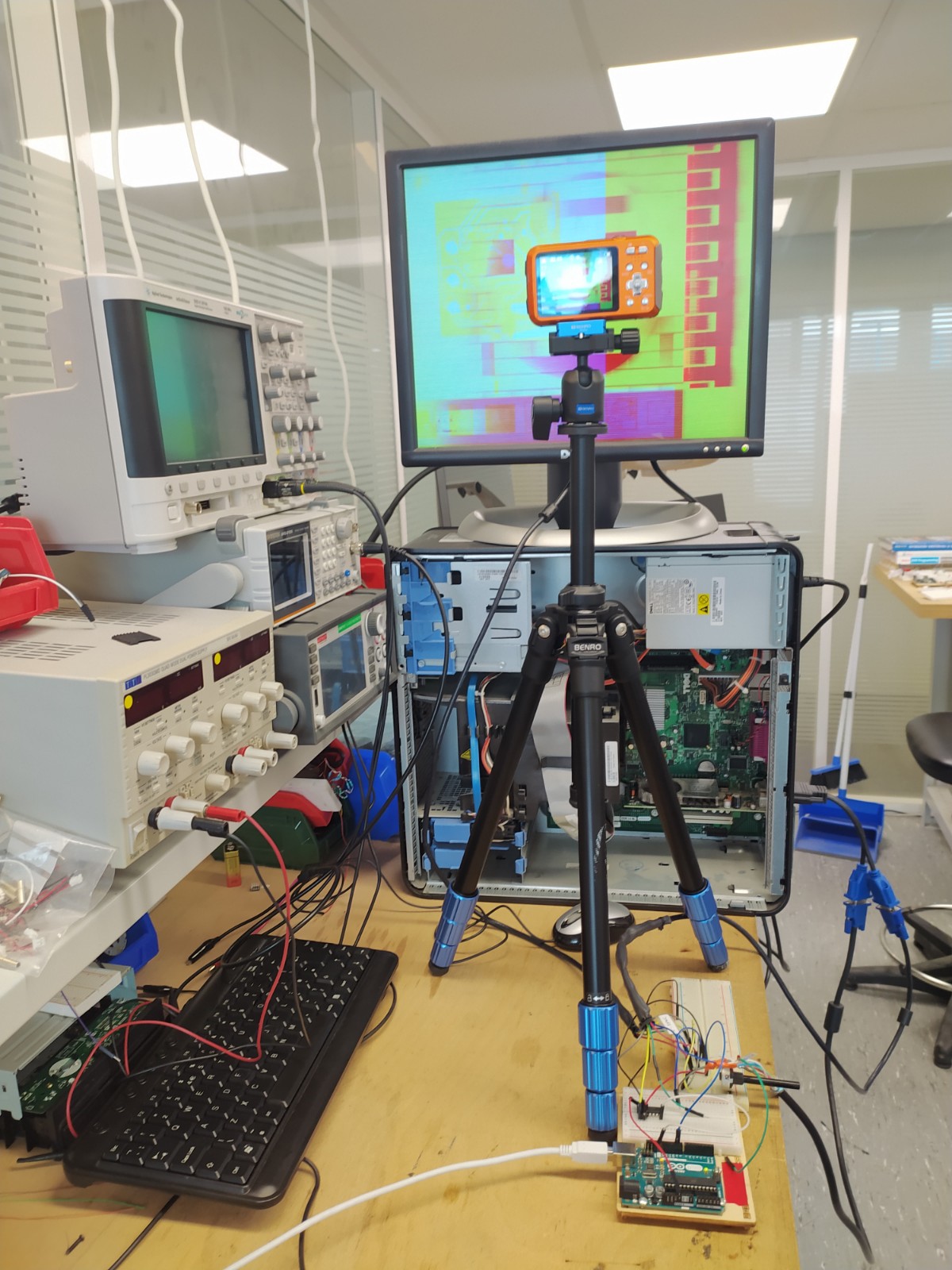
I have an older computer tower running Ubuntu which I opened to expose the video card, a small VGA compatible screen, and a camera setup on a tripod to capture the display. I have access to the lab’s IT team where I have been borrowing cables and getting my hands on some e-waste.
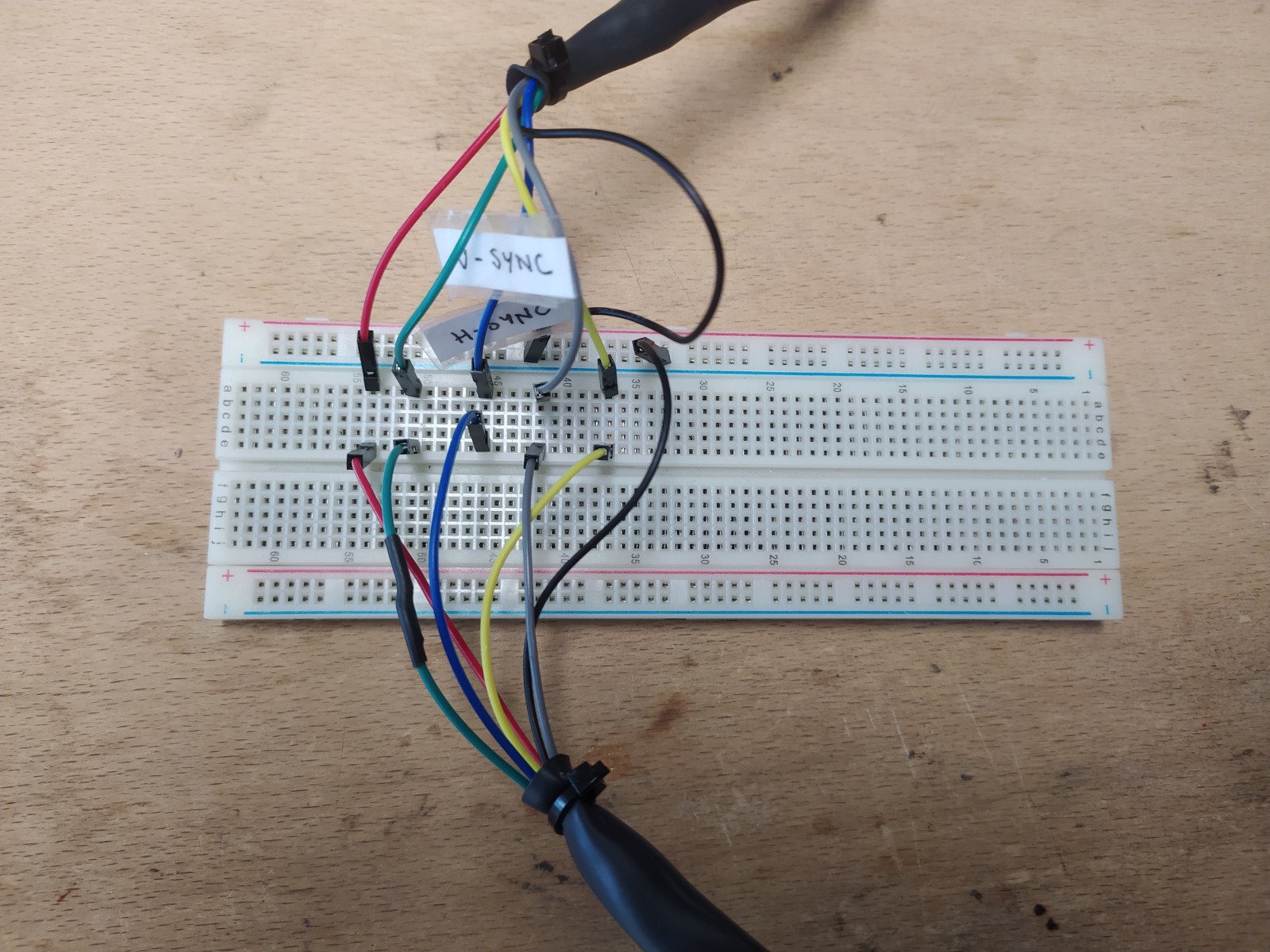
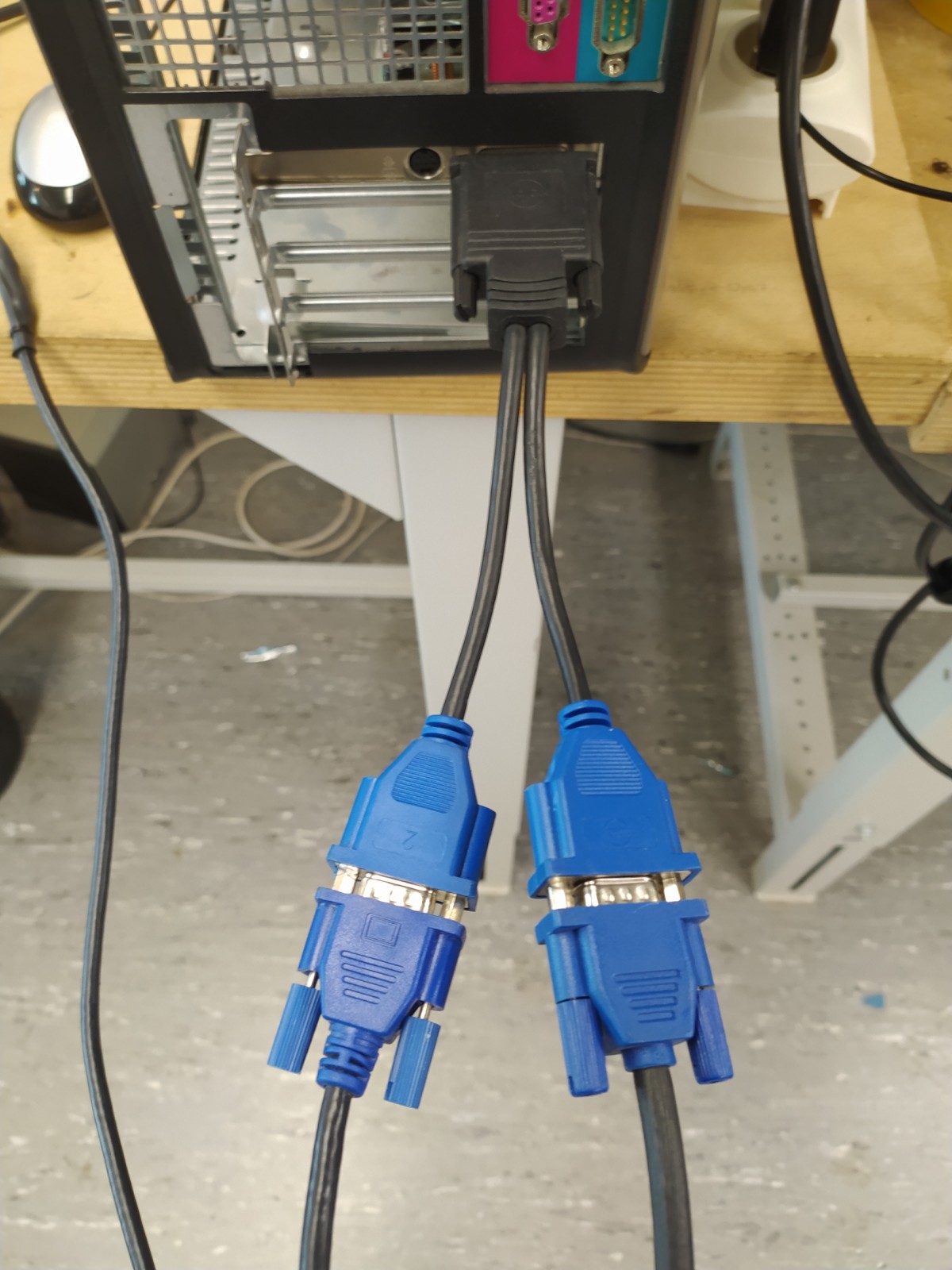
Experiment No. 1: VGA cable splicing¶

To begin understanding how VGA signals work, I took a VGA cable and split it down the middle. This allowed me to play with the different color channels and the two sync lines.
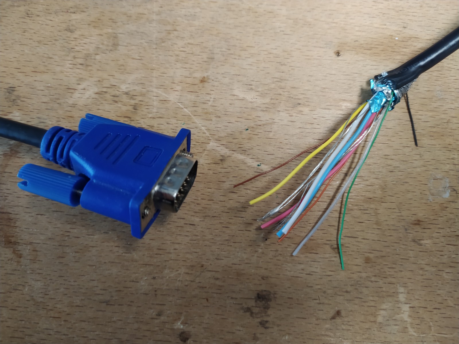
By just switching the connections between the channels I got a basic understanding of how things work. I played with: R,G and B (colors switching, colors adding together), unplugging ground (and getting some fuzz), unplugging V-sync and H-sync (the screen turns off).
Experiment No. 2: Mixing two VGA sources¶
I set up my computer to think it has two monitors of the same resolution, and then put two static images on each screen. I then spliced another VGA cable and then played with mixing the various channels (eg. plugging in red from one source and green and blue from another, etc,).
Experiment No. 3: Dirty Mixing¶
I have a potentiometer that I’m using to mix between various signals. The most interesting so far is to see how much the V and H syncs can be bent before the screen shuts off. I can at most move the display a few inches to one side or the other.
This very simple, but effective, idea comes from Karl Klomp: http://www.karlklomp.nl/

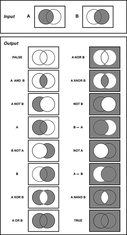
Experiment No. 4: Logic ICS¶
Looking at this venn diagram of logic gates (from wikimedia commons) combinations you can see how two signals can be mixed in different ways :
Inverting a color channel as input for the VGA screen.
Using a arbitrary function generator outputting a square wave XOR’ed with a color channel as input for the VGA screen. I’m using the 74LS86 chip. Things are already getting nice and messy.
Experiment No. 5: Noise¶
I added a simple arduino random noise generator to my VGA cable spliced set up to contaminate the signal.
long randNumber;

void setup() {

  randomSeed(analogRead(0));
  pinMode(3, OUTPUT);


void loop() {

}
  randNumber = random(300);
  analogWrite(3, randNumber);
  delay(1);
}

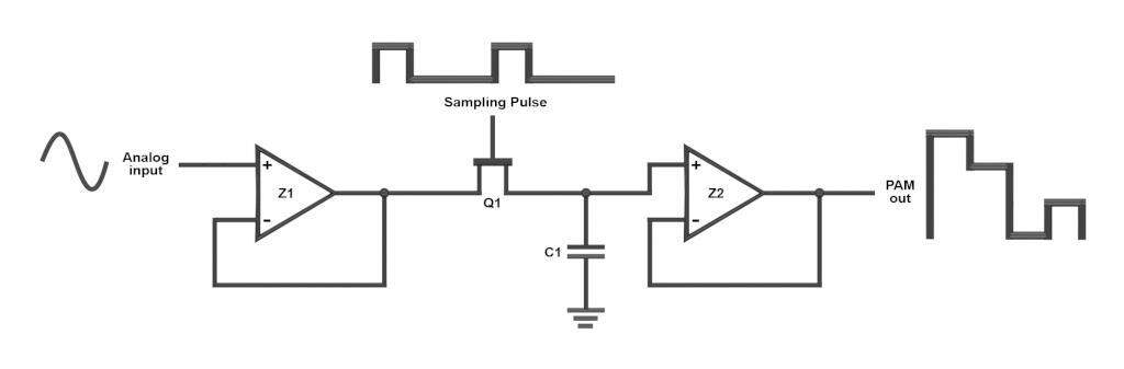
Experiment No. 6: Sample and Hold¶
Using a arbitrary function generator outputting a square wave to trigger a sample and hold with a color channel as input for the VGA screen. I’m using a pair of MCP6241 op amps and a generic MOSFET along with a .1 uF cap for the sampling.
From EEV site online:
Experiment No. 7: Arduino VGA library¶
Following these two tutorials (https://simple-circuit.com/interfacing-arduino-vga-example/ and https://learn.adafruit.com/adafruit-gfx-graphics-library/overview) I have arduino generating the V and H sync signals and outputting text. I appear to be limited to 160x80 pixels though, which is less than half my screen. When I try to add more pixels it says I’ve run out of memory.
I have also messed with the timing of the V and H sync to see how much bending is possible here. It turns out not much…

I eventually switched to the VGAX library (https://github.com/smaffer/vgax) which can control more pixels.
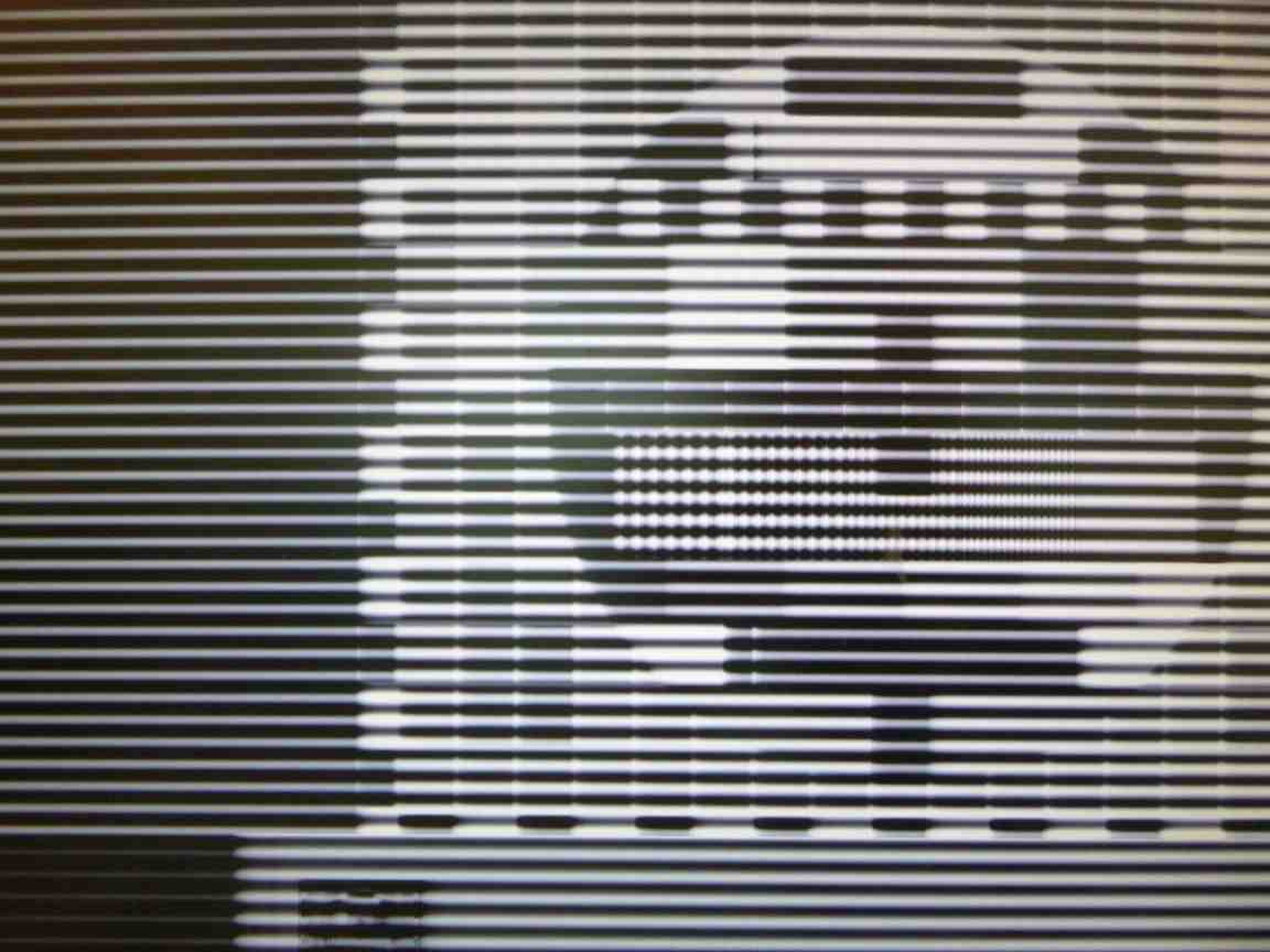
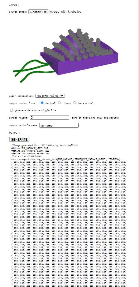
I used the included 2bitimage.html tool to take an image scaled to 120x60pixels and convert it into an array compatible for arduino.
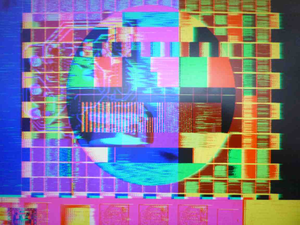
Here is what it looks like on the screen:

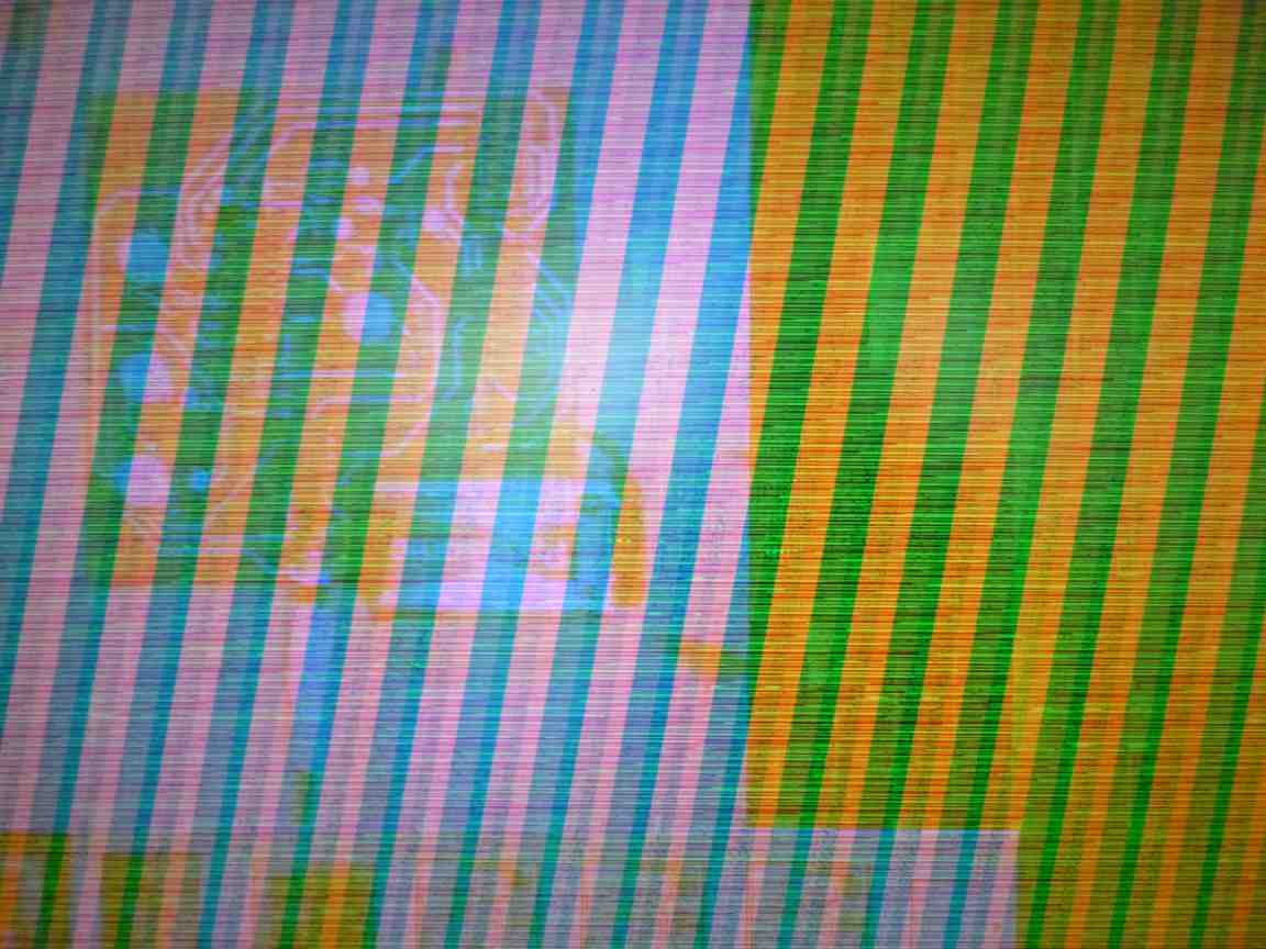
I currently plan to make a series of very simple “masks” that divide the screen vertically (it appears to be easy to generate horizontal patterns with circuit bending but less so vertical ones) or diagonally. These could be used to superpose multiple images at once and could be a feature of the video synth.
Experiment No. 8: RGB with oscillators¶
Here I have the computer generating the V and H sync signals and I’m synthesizing the RGB colors directly using a pair of oscillators.

Experiment No. 9: Audio Synth ICs¶
I ordered a handful of ICs from Banzai music (https://www.banzaimusic.com/) and plan to put images through some audio sound effects.
This article describes the effect of putting image data through Audacity : https://questionsomething.wordpress.com/2012/07/26/databending-using-audacity-effects/
I started with this Flanger from Electric Druid (https://electricdruid.net/wp-content/uploads/2015/06/4KNOBFLANGEDatasheet.pdf)
Here are some samples of the output:
Experiment No. 10: Selecting Video Clips¶
Looking at other video synths I realized that the video clips that were selected also had a big impact on the end result. I set up an array of gifs on two screens to mix with:

Here are the two screens with four gifs each:
Here is a sample output:

Experiment No. 11: GPU Circuit Bending¶
I am inspired by the artistic tradition of of circuit bending, https://en.wikipedia.org/wiki/Circuit_bending.
Here is an example using a GPU from user ZombieCarWash:
It’s hard to get inside my computer to bend the GPU. It would be great to have a PCI extender but our IT department doesn’t have any in stock.
I first tried removing the fan and heat sink so that I would have better access to the ‘chipy’ side but no luck - without this the GPU overheats dangerously in a matter of minutes.
I took photos of both sides of the GPU and am inspecting the traces. I know that I want to avoid making a short and that bending usually requires grounding connections. I looked up the names of various ICs and deduced that those zones were for power conversion and that they were to avoid:
I took precautions here, I connected a pin to ground of the graphics card and had a magnetized helping hand to hold the probe so I could position it on the GPU. I only probed the zone around the DDR RAM and not anything relating to power conversion.
Here is my set-up:
I later moved to a finer probe:
Here is the one glitch I managed before the old card stopped working:

I couldn’t be more pleased with the timing of the glithch vis-a-vis the gif!
Experiment No. 12: Floppy Disk Storage Media¶
EDIT This particular experiment proved to be very time consuming and, beyond learning a lot about old school magnetic storage media (and it’s limits for higher speed/data requirements video recording and playback) and using the voltage controlled oscillator, it didn’t directly translate into the final project in its current iteration.
After experimenting with vga signals, it feels too gratuitous and the colors are garish. Mixing samples with mod synth effects most interesting perhaps. Pure synthesis pretty in black and white but gets old.
I am shifting focus to historical pc media as inspiration, in line with my earlier experiments.
I am considering a video synth composed of two floppies, (four sides, one minute of recording) this way you can capture video samples and then mix them together, rerecord modified samples.
A second idea is to have just one floppy and very every single parameter modifiable (in the spirit of forensic, media archaeology):
Speed of motor spindle + scratchable Over writing or not (tunnel coils) Read/write head direction and speed Input + signal carrier frequency
This great project is an inspiration showing how to make an echo effect with an old floppy disk:
I’ve seen similar cool projects hacking tape decks to make loopers also:
Here is some good background on floppy hardware: https://info-coach.fr/atari/hardware/FD-Hard.php
And this is a rich forum for information about this project: http://forums.openmusiclabs.com/viewforum.php?f=11
I am following the floppy disk pinout here to guide my tests: https://amiga.robsmithdev.co.uk/instructions
(I have Arduino’s GND connected to the GND of the powersupply.)
To turn on the floppy motor: Motor Enable B (16) - LOW
To turn on the stepper motor that controls the head : Drive Sel B (12) - LOW, Step (20) connect directly to Index (8) (when disk motor is spinning) to use the pulses (thanks to first video link for this idea), Direction(18) to + or - to change direction.
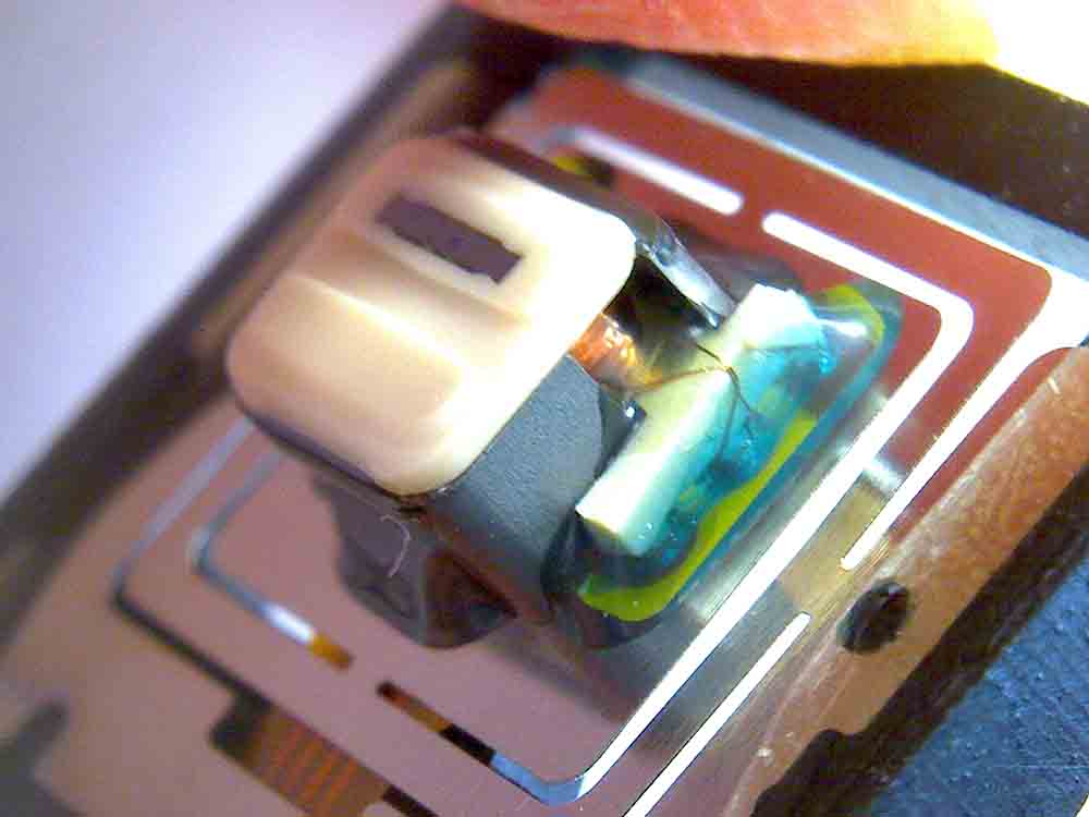
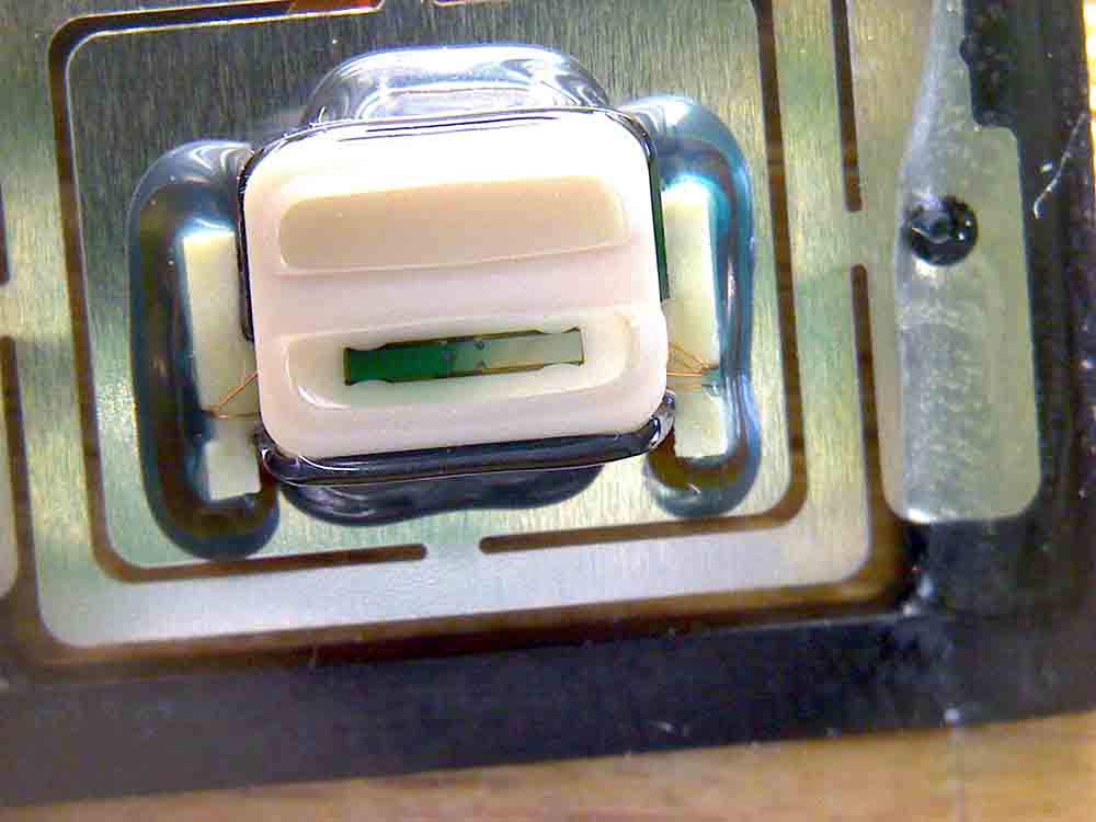
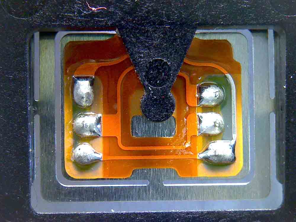
For the magnetic tape writers/readers, I see five pins for each head. To facilitate experimenting with the head I made this adapter by desoldering the head connector :
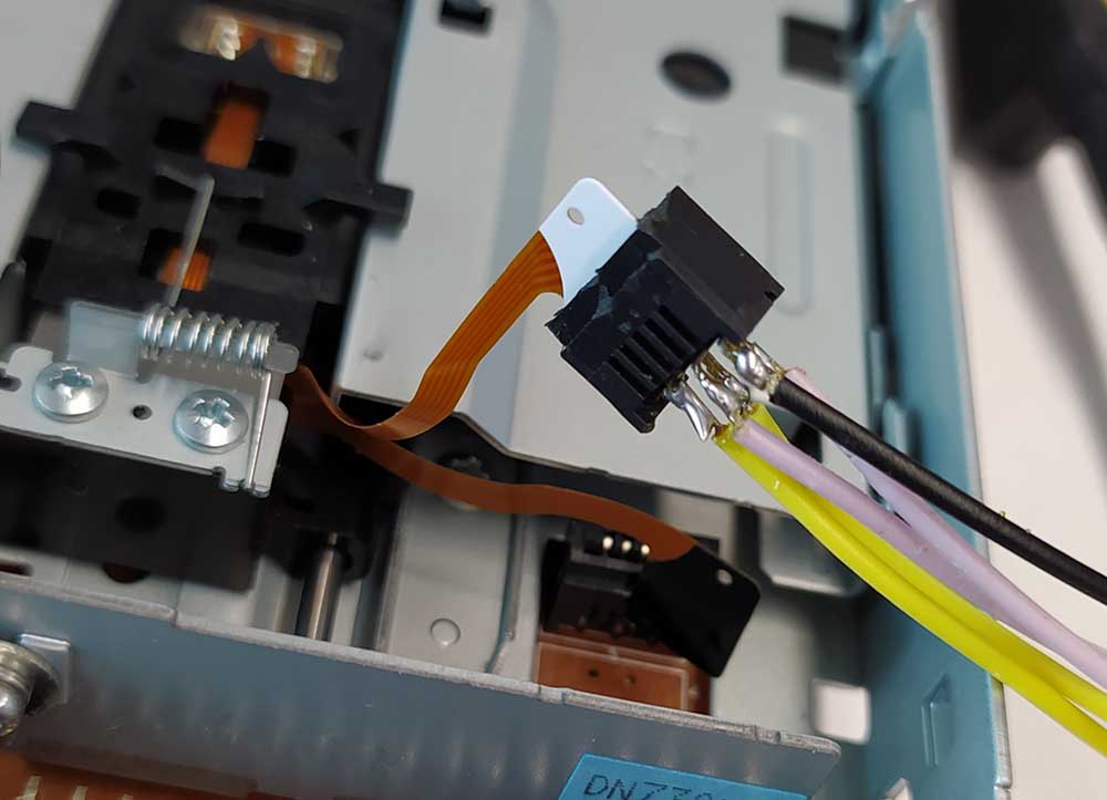
Some diagrams explaining the architecture of the Read/Write head I found online:
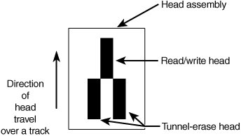
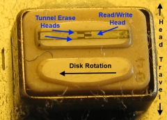
Here I’m trying to identify the write coil (the other two coils appear to be for limiting the spillover to adjacent tracks and are known as Tunnel Erase Heads)
I tried having two arduino outputs flipping between HIGH and LOW connected directly to what I believe to be the write head. I don’t seem to be writing anything to the disk and the two floppies I have appear to be blank if the oscilloscope is indeed showing me what’s going on here…
Several versions of this floppy hack involve connecting a tape player head directly to the floppy head. This appears to be because the tape already modulates the audio signal in a way that optimizes it for this kind of tape recording.
This project https://kaput.retroarchive.org/sampler/ does not talk directly to the Read/Write head but instead writes signals through the control circuitry on the board.
Here is the schematic from the site:
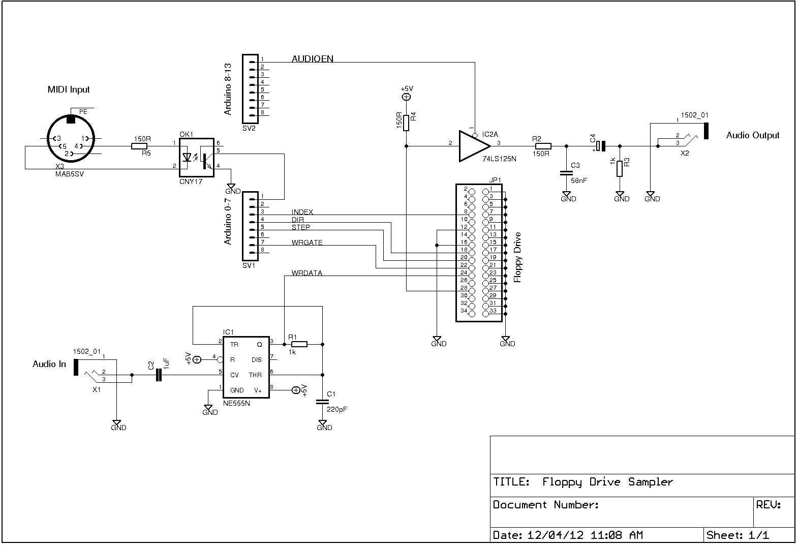
The input still needs to be modulated though. The 555 is producing the correct carrier frequency. I rebuilt the circuit in falstad and it seems to be around 10KHz (https://tinyurl.com/ycco7xaj). Elsewhere I’ve seen 40KHz up to 60KHz. Following the schematic provided on this site, it appears that to send data to be written the following pins need to be set:
Write Data (22) - LOW EDIT I later discovered this is not correct (this is in fact the DATA input pin) Floppy Write Enable (24) - input data modulated at the correct frequency EDIT I later discovered this is not correct (this is in fact the DATA ENABLE pin)
*(There appears to be an error in this schematic which shows pin 28 Write Protect pulled HIGH through a 150 ohm resistor, but this must be pin 30 Read Data pin instead because it’s the output and needs to be pulled up)
The signal can be read directly from the Read Data pin (30) which requires a pull-up.
++++++++++++++++++++++++++
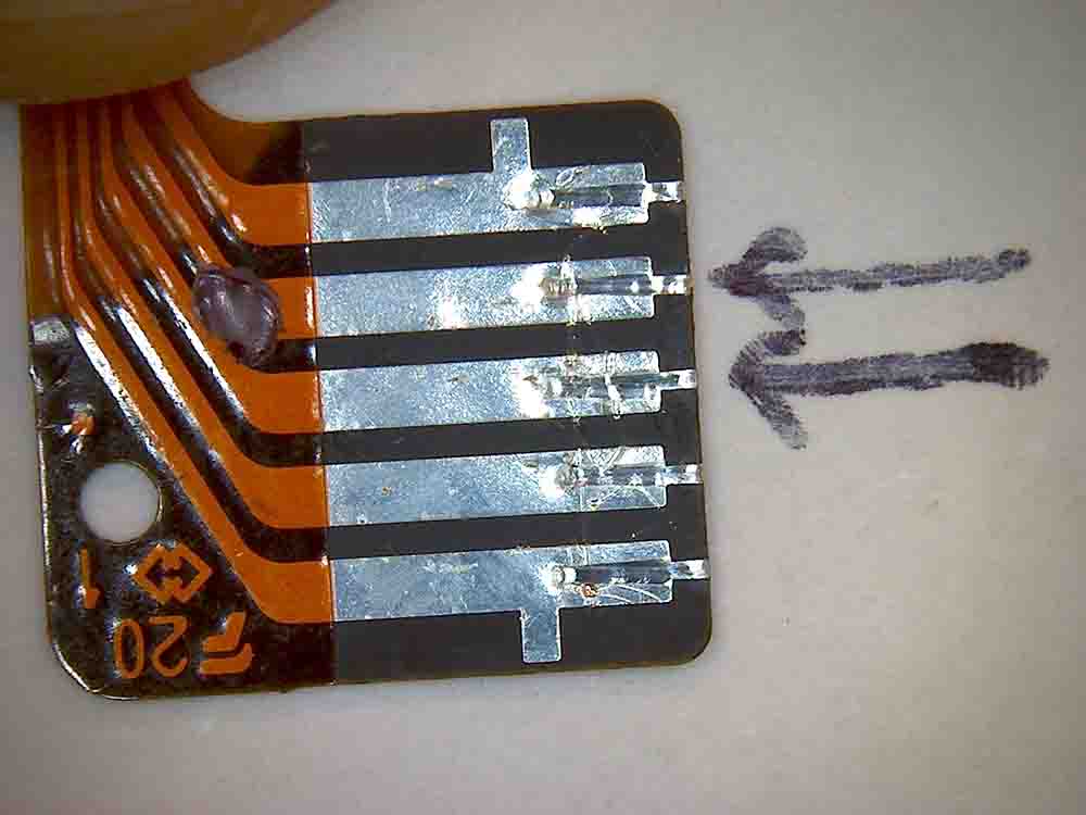
Following this tutorial (http://forums.openmusiclabs.com/viewtopic.php?f=11&t=92) I think I’ve decoded the pinout of the five pins from the Read/Write head. I’m assuming that BD is the Write head and that ABC is for the Tunnel Erase Heads ?
Here is my thinking currently:
Get tape head output and connect it to floppy head while playing tape. If this doesn’t work, function generator sine mode plus AND with Arduino random as input or audio input. If this doesn’t work 555 circuit as described on site + audio.
-I tried identifying the “data” pins from the tape player without success. I just had a bunch of what appeared to be noise? -I tried the 555 circuit which produced a 40kHz signal but it didn’t seem to be effected by the input audio. Also, I couldn’t see any evidence it was being written to the floppy. (Also, it seems that the real write data pin is 22, not the data gate or Floppy Write Enable at 24)
I moved to the code provided by RobSmithDev here https://github.com/RobSmithDev/ArduinoFloppyDiskReader and following the wiring I can seek to different tracks and read data at each track. However, rereading the same track data produces different results. I’m not sure if this relates to the tape reader I removed, but I am setting the lower tape head so I don’t think that would be a problem. Erasing tracks also doesn’t appear to work.
Here is a sample of the kind of madness I am reading :
!1ªZÕVª¦^šjªf^šj§j§v©©v¶í—fÝyifjZ×y¦^m§wjÕïv]zmemךþmvj×u�ö×^Õéo^mÖf¥j×]UÖk^Ù•uU][Y•ÕýZ›zÙÝþ§Vþëï_ßí§^íev¿æ¿½í§o^íÿ¾ïÙÕ^æwU^ukçç¥VUUU]WUW]šŸÙUU¥Wvi•Z©–Z©•Z©•©ªZ©•Z•UUUUUUUUUªªUµk•Uui�ujWeU—›ZZ�•e[õZWYeZVUUU¥™giZÙ¥Y•Ui•j]ve¥f�ºYší^u¥U¥[veuuf§gjU•¦fUuuU•]µv—Z™ZUu™Vf™Uu¥•UZ©jVUeeUu]–––W•Û—VYWU–ÖiÖWfÖi¹¥UåWuVZUgW¥¥eUåeÛU¦»•WÝYeV¥VeUUVe×U�WUUV•YVÕzue•—f×}•¶Y•UjªšVš•VU•UY–VZYeµYVV™UuWiUu{Vf}]ešVueWiUU¥]•ª•k�f¹Z¥[ÝZW¶«YYje]wÕU–fuUVVVViUU¥UZ¥y•Vi™UUVVV¥Y›žUÖ©iU¥UfZU¥WUšYe®jU••ÕßWu®Ve_µU©VmYVžþÙÕZWUUf¿U}•éjjÕ]U}iiWú¦W–VVîšWu–nuÙW•µWYVZf¥«WZ•zV�•UmWµ›VWVU_iU•UWUf{íWfUU×umYwv««¶º«z—z©—š©º—š©™zi™š—š©™š©YZ©j©™j©™š©š©•š©™š©š©•j©•j©Z©•Z©UUUUUUUUUUæªU¥U•–¥Z©•©•j©•Z©•©–Z©•ZUUUuUUUUUUW�_UYiVe•§VVufU¥e·UWÕí—µÕ¥uÕ¥šUU•¥UuÕYiVuÝV�–©ÕVUÞ™V®jÝiii¦]V}U•¹uYyu}VZZ™é]j¶VeYÝeUÙªW}½f™¥YZWgÝ¥U¥Uå§W«ee[–_ª™VeåY–�{UYfiº¶›—^yVU]YzvV™V™VÚ–U[WUjin–éU]jVf×¾ªåUZgeÙžWgf^jvÙ—éÚÕ–ùîeµU©iVVæ•]VWÕgjšUf—uú¿¹f]©VõÞYÚúu¥[U¯õ¦iÕ•¥¹Uš—i¶Ùuu•�u¥eUjg©yU–U¦UVÕUfªoߥYVv–µeUUy®ee_æi§ªkgV^UmUy©j•V™]eV¶¦VUzUYWZ§U�¥UeYuVµªµjeÚÕw_uªWªåy[zç•VçVµu¦×–Úê}©·ÝÙ©V¥–™¯ÖÚª•zµ¯»g©Zii]¥UU•nå]UU�ivg—¶VUuUu©iîÖ~f—�Wyzºº««kzkº©z©—z©—v©�z–š©™š©™š©™©™–©™š©•©™š©™š©™©•š©™Z©•©•Z©–Z©•©UUUUUUUUU[ººV¥UZV©Z©•Z©•©•Z©•Z©Z©ejUUUUUVUUVUûWåUöiWªUZeVUe¥W¯VU]]Þ×µZYUå¥jUY_Vzuu¥¦VvV�–�ÕeVéVi–Z¥UÖ•eéU©y••õUVi}m«š®uÛ
I still can’t see anything intelligible going on on the oscilloscope listening to the READ pin…
I am using these commands from the Arduino Floppy Controller (not the windows interface):
// Command: "?" Means information about the firmware
case '?':writeByteToUART('1'); // Success
writeByteToUART('V'); // Followed
writeByteToUART('1'); // By
writeByteToUART('.'); // Version
writeByteToUART('7'); // Number
break;
// Command "." means go back to track 0
case '.': if (!driveEnabled) writeByteToUART('0'); else {
if (goToTrack0()) // reset
writeByteToUART('1');
else writeByteToUART('#');
}
break;
// Command "#" means goto track. Should be formatted as #00 or #32 etc
case '#': // Goto Track
if (!driveEnabled) {
readByteFromUART();
readByteFromUART();
writeByteToUART('0');
} else
if (gotoTrackX()) {
smalldelay(100); // wait for drive
writeByteToUART('1');
} else writeByteToUART('0');
break;
// Command "[" select LOWER disk side
case '[': digitalWrite(PIN_HEAD_SELECT,LOW);
writeByteToUART('1');
break;
// Command "]" select UPPER disk side
case ']': digitalWrite(PIN_HEAD_SELECT,HIGH);
writeByteToUART('1');
break;
// Command "<" Read track from the drive
case '<': if(!driveEnabled) writeByteToUART('0');
else {
writeByteToUART('1');
if(disktypeHD)
readTrackDataFast_HD();
else
readTrackDataFast();
}
break;
// Command ">" Write track to the drive
case '>': if (!driveEnabled) writeByteToUART('0'); else
if (!inWriteMode) writeByteToUART('0'); else {
writeByteToUART('1');
if(disktypeHD)
writeTrackFromUART_HD();
else
writeTrackFromUART();
}
break;
// Command "X" Erase current track (writes 0xAA to it)
case 'X': if (!driveEnabled) writeByteToUART('0'); else
if (!inWriteMode) writeByteToUART('0'); else {
writeByteToUART('1');
if (disktypeHD)
eraseTrack_HD();
else
eraseTrack();
}
break;
// Command "H" Set HD disk type
case 'H':
disktypeHD = 1;
writeByteToUART('1');
break;
// Command "D" Set DD or SD disk type
case 'D':
disktypeHD = 0;
writeByteToUART('1');
break;
// Command "M" measure data timings
case 'M': if(!driveEnabled) writeByteToUART('0');
else {
writeByteToUART('1');
measureTrackData();
}
break;
// Turn off the drive motor
case '-': digitalWrite(PIN_DRIVE_ENABLE_MOTOR,HIGH);
digitalWrite(PIN_WRITE_GATE,HIGH);
driveEnabled = 0;
writeByteToUART('1');
inWriteMode = 0;
break;
// Turn on the drive motor and setup in READ MODE
case '+': if (inWriteMode) {
// Ensure writing is turned off
digitalWrite(PIN_DRIVE_ENABLE_MOTOR,HIGH);
digitalWrite(PIN_WRITE_GATE,HIGH);
smalldelay(100);
driveEnabled = 0;
inWriteMode = 0;
}
if (!driveEnabled) {
digitalWrite(PIN_DRIVE_ENABLE_MOTOR,LOW);
driveEnabled = 1;
smalldelay(750); // wait for drive
}
writeByteToUART('1');
break;
// Turn on the drive motor and setup in WRITE MODE
case '~': if (driveEnabled) {
digitalWrite(PIN_WRITE_GATE,HIGH);
digitalWrite(PIN_DRIVE_ENABLE_MOTOR,HIGH);
driveEnabled = 0;
smalldelay(100);
}
// We're writing!
digitalWrite(PIN_WRITE_GATE,LOW);
// Gate has to be pulled LOW BEFORE we turn the drive on
digitalWrite(PIN_DRIVE_ENABLE_MOTOR,LOW);
// Raise the write gate again
digitalWrite(PIN_WRITE_GATE,HIGH);
smalldelay(750); // wait for drive
// At this point we can see the status of the write protect flag
if (digitalRead(PIN_WRITE_PROTECTED) == LOW) {
writeByteToUART('0');
inWriteMode = 0;
digitalWrite(PIN_DRIVE_ENABLE_MOTOR,HIGH);
//digitalWrite(PIN_WRITE_GATE,HIGH);
} else {
inWriteMode = 1;
driveEnabled = 1;
writeByteToUART('1');
}
break;
case '&': runDiagnostic();
break;
```
I switched to the AVR Studio Port listening software because it allows me to select exactly 2000000 BAUD and now I can erase tracks (but rereading the same track still produces different data..)
I can go from this: §•UfUe–YjUåî_UUeVUUueY•Y§U•Ume¹ejªéYoùŸ–neVåU[å•Öêåe
to this: UUUUUUUUUUUUUUUUUUUUUUUUUUUUUUUUUUUUUUUUUUUUUUUUUUUUUUUUUUUUUUUU
The sequence I'm following: 0.) D for disk type, and then [ for the lower part of the disk (I desoldered the head for the top part of the disk earlier) 1.) + : turns on spindle motor in READ mode 2.) #44 : go to track 44, say. 3.) < : read the data here. 4.) ~ : switch into WRITE mode, 5.) X : erase this track, 6.) + : back into read mode, 7.) < : read what is on this track.
This appears to work even if I go travel elsewhere and then come back to this same track. I'm guessing my earlier experiments left a bunch of unreadable stuff?
Next test: Can I write something other than U's, and, eventually take a stream of data to write. (If I switch to hex representation it's all 5s instead of Us)
I have just realized when I erase, the code writes the variable currentByte which is set to 0xAA (which is 10101010 in binary). I'm reading it as 0x55 in binary is 01010101 - i.e. there is an issue with bigendian versus littlendian. *EDIT* (I just read in the code that two '1' arent allowed in a row on a floppy...)
I can send currentByte 0x0F but because everything is seemingly getting shifted around a bit I get a lot of Fs. I think I get the logic behind writing 01010101... because the floppy medium works with changes in flux. I also notice I have to type several times < to get the reading. I still read slightly different things when I reread the same track.
+++++++++++++++++++++++++++++++++++++++++++++++++++++
I am starting to realize that VGA timing protocol etc. is its own project. I could bend this protocol and make a project around it. However, the floppy disk is its own system. To experiment with it, I would need to explore the limits possible within it. To visualize the memory (as it is not tied to a visual representation form like other peripherals), I could have a simple processing program that reads the disk memory and draws a bitmap. Over reading/recording cycles, the data would rot, and you could visualize the rotting. It would have knobs for all the parameters of the floppy drive. This could work because the data is not encoded and there are no protections (check sums etc.).
I just tried the amiga arduino floppy setup with FTDI cable and can at least get passed the Diagnostics. I can write without verifying as well. However when I try to read the data and save it to file I get the following error: disk has checksum errors/missing/damaged data. When I try to write with verify I get Verify error.
I swapped out the floppy drive I had been experimenting on these last few days for a new one and retried:

I can also write and read files with Verify Write:

This process isn't flawless and I have to rewrite and retry often to get it to work, BUT it can write text to the floppy and then read from the disk and find the same text.
This doesn't appear to work in the Arduino only interface however. Here I guess I am writting un encoded data, without checksums etc., that the Amiga windows program does. This would explain the lack of stability perhaps. I'm also pretty sure it's also reading the data backwards somehow.
+++++++++++++++++++++++++++++++
I'm not sure where to go from here. I can reliably read and write to the floppy disk but...this you can also do with any computer!
I think it would be cool to get arduino reading/writing files to the floppy WITHOUT a computer. The data could be from a sound/video input and the output could be the same.
I think the first step would be gut the Amiga code to just the portions that write and read on the Arduino, and scrap all the USB communication parts. If I could get arduino alone to erase a disk, and then output the data that would be a first step.
Here is the code that erases a track:
// Write blank data to a disk so that no MFM track could be detected void eraseTrack() { // Configure timer 2 just as a counter in NORMAL mode TCCR2A = 0 ; // No physical output port pins and normal operation TCCR2B = bit(CS20); // Precale = 1
register unsigned char currentByte; //this is the byte that actually gets written

// Enable writing
PIN_WRITE_GATE_PORT&=~PIN_WRITE_GATE_MASK;

// Reset the counter, ready for writing
TCNT2=0;
currentByte = 0xAA;

// Write complete blank track - at 300rpm, 500kbps, a track takes approx 1/5 second to write.  This is roughly 12500 bytes.  Our RAW read is 13888 bytes, so we'll use that just to make sure we get every last bit.
for (register unsigned int counter=0; counter<RAW_TRACKDATA_LENGTH; counter++) {
    WRITE_BIT(0x10,B10000000);
    WRITE_BIT(0x30,B01000000);
    WRITE_BIT(0x50,B00100000);
    WRITE_BIT(0x70,B00010000);
    WRITE_BIT(0x90,B00001000);
    WRITE_BIT(0xB0,B00000100);
    WRITE_BIT(0xD0,B00000010);
    WRITE_BIT(0xF0,B00000001);
    while (TCNT2>=240) {}
}

// Turn off the write head
PIN_WRITE_GATE_PORT|=PIN_WRITE_GATE_MASK;

// Done!
writeByteToUART('1');
digitalWrite(PIN_ACTIVITY_LED,LOW);

// Disable the 500khz signal
TCCR2B = 0;   // No Clock (turn off)
}
The write from serial has a serial buffer and the current byte moves up through it:
currentByte = SERIAL_BUFFER[serialReadPos++];
…
    while (TCNT2>=240) {}

    // Now we write the data.  Hopefully by the time we get back to the top everything is ready again
    WRITE_BIT(0x10,B10000000);
    CHECK_SERIAL();
    WRITE_BIT(0x30,B01000000);
    CHECK_SERIAL();
    WRITE_BIT(0x50,B00100000);
    CHECK_SERIAL();
    WRITE_BIT(0x70,B00010000);
    CHECK_SERIAL();
    WRITE_BIT(0x90,B00001000);
    CHECK_SERIAL();
    WRITE_BIT(0xB0,B00000100);
    CHECK_SERIAL();
    WRITE_BIT(0xD0,B00000010);
    CHECK_SERIAL();
    WRITE_BIT(0xF0,B00000001);
I could just read data on an analog pin, map it to byte range, and store it in an array. Then I could write the array to the floppy disk using the write from serial code? The first step testing this idea would be to make an array of values and then write them to the floppy. I would then need to demodulate on the read side...Or possible just read from the register that is used to store the data sent on the USART called DataOutputByte ?

In terms of timing, there is TCNT2 an TCCR2B which is described as a 500khz signal. What pins are the timers outputting to? Could I manually generate this frequency in order to write similar to the 555 circuit.

The WRITE_BIT code also seems to use the hex values for timing:
// Small Macro to write a ‘1’ pulse to the drive if a bit is set based on the supplied bitmask #define WRITE_BIT(value,bitmask) if (currentByte & bitmask) { \ while (TCNT2<value) {}; \ PIN_WRITE_DATA_PORT&=~PIN_WRITE_DATA_MASK; \ } else { \ while (TCNT2<value) {}; \ PIN_WRITE_DATA_PORT|=PIN_WRITE_DATA_MASK; \ } ```
# Experiment No. 13: Floppy Disk Storage Media Continued
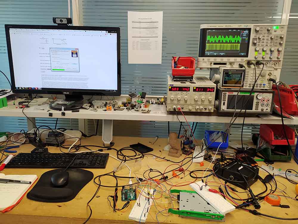
Here is my current setup:
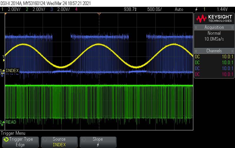
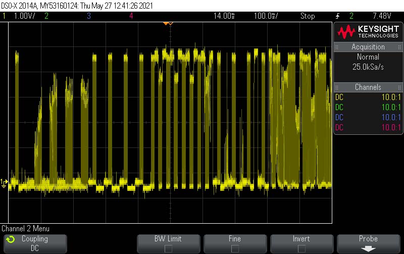
I checked out what frequency the floppy disk set-up I had working was sending signals at:
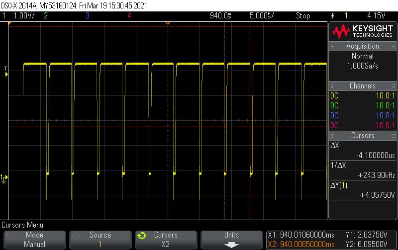
It appears to be around 250kHz. In the code they mention something around 500kHz so perhaps this is half?
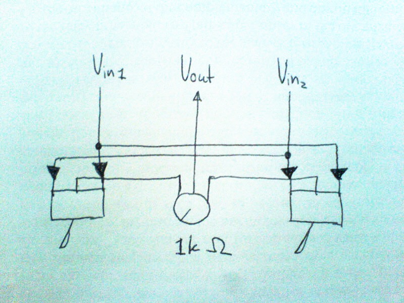
I used the arbitrary function generator along with the probe testing signal on the oscilloscope and two 1K resistors to make a summing circuit. It looks like this:
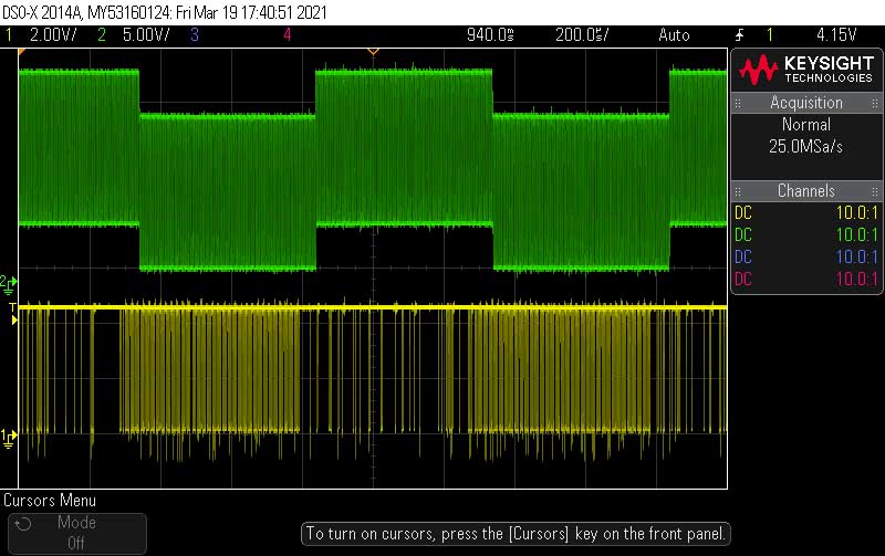
Basically the 250kHz signal rides along the 1kHz (?) lower frequency oscillator from the oscilloscope (this is green on the oscilloscope).
The yellow is plugged in to the READ pin and the green is the INPUT when the floppy disk is in write mode. I think it is working but I’m not sure.
I next took sound output from my phone and passed it through a battery powered amplifier, and then summed it with the 250kHz signal from the arbitrary function generator. Again green is the INPUT and yellow is the READ. I don’t get the impression it’s working…
To test if the music has somehow been frequency modulated into the output when reading, I have a low pass filter set to a 100kHz cut off (150ohm resistor plus a 10nF cap). I want to cut out the carrier frequency and see if I can get the signal that’s riding on it.
Unfortunately I have some kind of noise issue that is now preventing the floppy from operating normally…
++++++++++++++++++++++++++++++++++++++++++++++++
I rewired everything as neatly as I possibly could and no longer have any noise issues !
I have my oscilloscope set up to listen in to the READ and the WRITE while I still use the Arduino Amiga Floppy Disk writer software and firmware.
Check out this awesome video by user kitsune-denshi https://www.youtube.com/watch?v=ziVXF_tM4Gw which shows how to write digital data to an unmodified floppy drive by modulating and demodulating using a CD74HC4046A PLL! The idea is to use a VCO to convert music or RGB information from a VGA into a modulated frequency in the right range to be recorder on the floppy. When reading from the floppy, the PLL of the 4046 demodulates and produces an error signal which corresponds to the input signal.
After watching this I got started trying to wire up the VCO of my CD74HC4046A:
You set the VCO frequency with a capacitor and a resistor, give it an input signal and have a FM version of the signal at VCO out. I am looking for something like this on the scope sending a triangle wave with the arbitrary function generator :
Here is another version from Falstad: https://www.falstad.com/circuit/e-vco.html or here: https://tinyurl.com/yfqhnkrk
Looking at the datasheet, it looks like we should expect around 50kHz with a 10nF cap and a 10K resistor.
I am outputting a 1.5V amplitute triangle wave with a 1V offset at 500Hz and getting this on the scope:
I noticed when changing the frequency of the VCO input signal that there was a sweet spot :
Too low (under 100 Hz):
Too high (Above 2kHz):
Just right (around 500 Hz with the VCO tuned to around 50kHz):
I tried putting the raw signal on the write pin, and then read the contents but it doesn’t appear to read the signal I intended to write :
I’m guessing my signal (blue) doesn’t look enough like the signals being written (green). I think I need higher frequency FM signal.

# Experiment No. 14: 3D printing and laser etching circuits
I am making PCB versions of the breadboards I was experimenting earlier with:
Here it is ready to lasercut. It fits just on the stock size of PCB we have (101mm x 152mm). I am considering making this the size of the synth:
Here is the diagram of how it could all come together:
I also harvested some nice parts from this mixer:
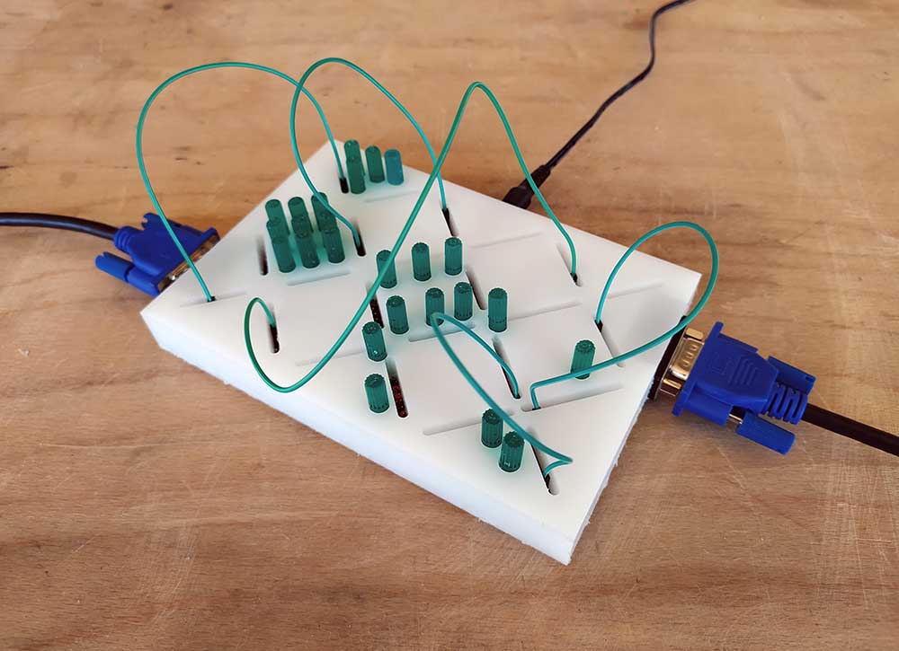
I am also printing this wavy surface on the 3D printer with holes that allows pots through as a test for the interface.
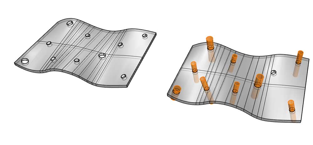
And here it is IRL:
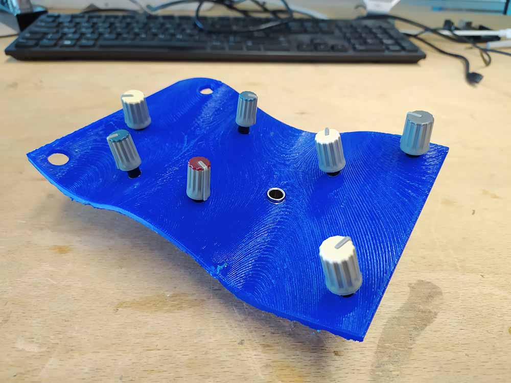
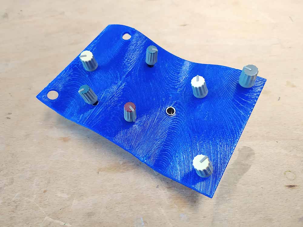
With jumpers:
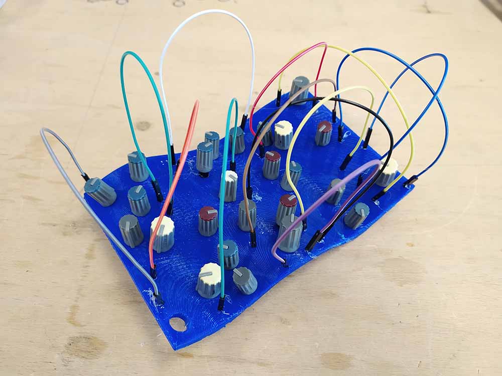
The idea would be to use female-female jumpers and insert linear headers in the wavy interface. It could be fun to make the composition of round knobs bending in different directions plus lines in different angles. I would also need to add text to this. The size of the curvy surface I think should be limited by the size of the PCB we have.
…and about recording video onto a tape cassette:
https://www.ubergizmo.com/2020/04/audio-cassette-tape-used-to-capture-video/
I tried connecting the READ and WRITE pins of the Floppy disk to the VGA color channel and got snow. Moving around the disk, writing etc. didn’t change the video image. This makes sense perhaps, as a floppy can only save several hundred bits of data per second and video requires millions of pixel information every second…
# Experiment No. 15: Moving beyond floppy black hole
I could have arduino trigger video clips on the computer by acting like a keyboard:
https://www.arduino.cc/en/Tutorial/BuiltInExamples/KeyboardMessage
I could try to push arduino graphics to the limits. Great videos using arduino to make 1 bit video:
https://www.gieskes.nl/visual-equipment/?file=gvs1
And the TV out library:
https://code.google.com/archive/p/arduino-tvout/
I could also try to find an old VIDEO tape recorder to tamper with from leboncoin:
https://www.leboncoin.fr/image_son/1974929199.htm?ac=2404136686
Assembling the new PCB here is my current thinking:

-I should test the AS3340 VCO on a breadboard (it has triangle, sawtooth etc unline the VCO I am using currently). EDIT It needs special voltage :(. -Try leonardo as keyboard to control video on the computer. (How program exactly?) EDIT Will just talk to Processing via serial to control video. Next question is if I can VGAX along with sending serial commands. -Make some masks and videos for the VGAX library. EDIT I won’t be able to use these masks with VGA input because they don’t share the same syncs… -Look into using binary counters (synchronized by the atmega somehow) to breakout all the counting up to V-Sync and H-Sync for plugging in to other stuff. EDIT Music with binary counting exists and it’s called Byte beat (thanks Karl Fousek for this tip).
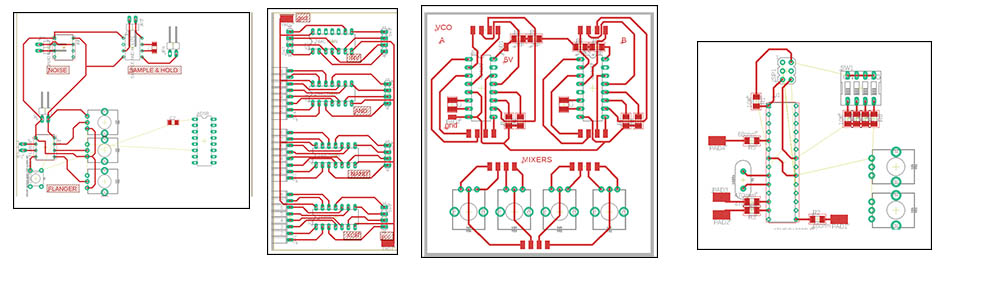
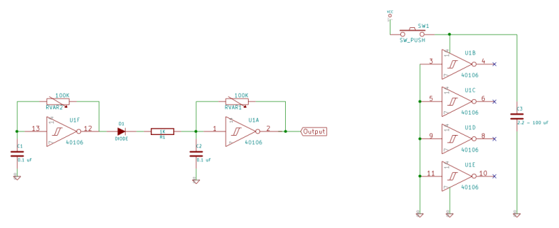
Experiment No. 16: Redesign of PCB¶
META ERRATA:
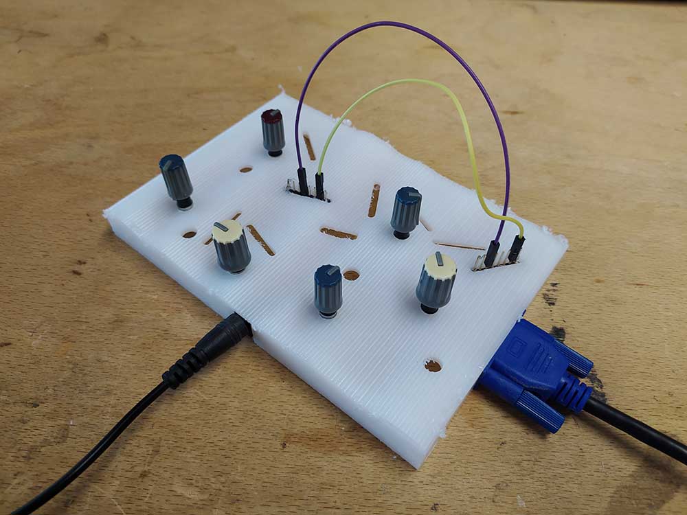
-To make this work with the CNC’d interface, I think I will need to change the size of the waviness of the HDPE block so that I can just add it on top of the PCB and just tilt the knobs.
-I can’t merge the signals from the VGAX board with the VGA signals coming from the computer as they have diff syncs. I could set up two modes, one for mixing and the other for generating signals from scratch. Or I could somehow set my computer’s screen resolution to the VGAX resolution…
-need to turn off screen sleep on computer I use!
-add text with nice font and possibly solder it to make it more visible.
-move knobs in non orthagonal grid, possibly other chips also (45 angles?)
PCB ERRATA:
MIXERS
-bit dark range in the middle where neither signal visible…(replaced 44K pot with 470ohm and it works well now so those harvested pots are only good for certain signals)
-so I need different pot values present for testing different patches?
VCO
-Pin 9 is a voltage level input, so I could also put a pot here to vary between 0 and 5V. (I could also have a trim pot to control the oscillation range ?)
-Adding a 556 Forrest Mimm’s atari punk console circuit and a ring oscillator with a pair of hex inverters. Would be cool to use the 8 bit switch somehow to select how many inverters to string together?
LOGIC
-could conceivably have just one or two sets of input with a knob that changes which boolean operation you want (that way you don’t need to replug).
-tie floating inputs down for logic chips
-use SMD logic chips to save space next time
-add binary counter in SMD! I have this chip in SO16 package : SN74HCT4020
-0.1uf next to each IC!
-symbolic representation of the logic gate on board
VGAX
-could have eeprom chip to save images ?
-how connect output of microchip to the VGA output and disconnect it with a single switch to let other signals pass? EDIT With buffers.
-I need caps on the crystal! It feels unstable and often needs reseting currently.
-I need cap next to IC
-I need 2x3 screw terminals for the 5 connections as VGA output
-reset button
-add UART connection and symbols for effect of pushing buttons (fast forward etc.) if this is possible to do while running VGAX code? EDIT Appears to after test with arduino.
-add pictures of diff masks
-need switch to put it into sending video controls versus making masks
POWER
-barrel connector with LDO
-power LED
-raw VIN with reverse protection
-on/off switch (possibly harvested)
-how connect all the powers together and should have isolation shunts?
INPUT
-mark very clearly what is an input and what is an output!! I could use diff color headers for each to make things very clear.
-another VGA out 6 screw terminals, or maybe two so that I can mix two images coming from the computer?
-connect H and V syncs directly across the board to the output by default ?
OUTPUT
-another VGA out 6 screw terminals
-audio jack out
-BNC out for oscilloscope
-add 460ohm resistors before any 5V signal going to VGA. Or add a trimpot so you can decide the risk you take for your screen depending on which signal you’re sending. I am finding that different patches require different output resistances so better to have the pot. (-I am sending 5V signals to the monitor via the VGA cable, but it should be between 0-0.7V. This wasn’t an issue before for me for some reason but then again I was using a differnt graphics card which may have been more resistant to abuse. Ben Eater explains how to calculate the resistance assuming that the interior of the screen has a 75ohm resistance. (At the 6 minute mark: https://www.youtube.com/watch?v=uqY3FMuMuRo) 0.7V = 5V (75ohm/R+75ohm), solving for R he gets: 460ohms. )
-do I need to protect the screen during the blanking phase after the syncs?
FANCY CHIPS
-flanger pins too close
-sample and hold appears to work at 5V so no need for shunts
OTHERS
-chose a better font for the text (courier new or a vector font)
-SMD headers anc IC holders!
-ground plane !
-hard to figure out what the optimal layout of the different subsystems is but that will need to come from testing.
-at least 4 standoffs
-test pads everywhere
-I need a power rail that isn’t linear but is star like going around connecting to all the modules. I want to use curvy wires.
-I could add a VCO with different waveforms possible. I could do this with at atmega328. I followed this instructable a while back which was perfect:
https://www.instructables.com/Arduino-Waveform-Generator/#:~:text=Waveform%20generators%20(also%20called%20function,for%20testing%20and%20debugging%20circuits.&text=This%20waveform%20generator%20is%20powered,in%20frequency%20from%201Hz%2D50kHz.
Experiment No. 17: Logic Noise¶
After reading this series of 12 articles on hackaday : https://hackaday.com/2015/02/04/logic-noise-sweet-sweet-oscillator-sounds/
I am now thinking about the possibilities of using exclusively inexpensive logic chips for my synth needs. I am putting in an order for some of the rarer chips used (unbuffered inverters, analog switches, etc.) and looking at SMD versions of all the chips I’m ordering. The idea is to make a minimalist design, just one VGA output, and possibly only in black and white. I want to follow their tutorial closely and see how well the world of audio synthesis will carry over to video (because the frequency is much higher for video pixels than for audible sound).
Zooming out, the idea is to make a board to experiment with the parameters of VGA signals (timing, blanking, analog R G B levels at pixel frequency). Together with the last board I’ll be able to test to see which chips work best together in order to make the final board.
This is what these signals look like:
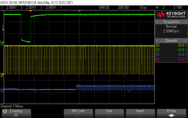
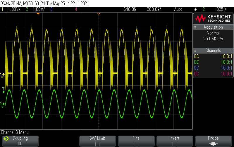
Here they are on my scope. The green is the vertical sync, the yellow the horizontal, and the blue is one of the color channels.

Of the logic chips I have that are interesting for generating signals for this project I have a:
- 14 stage binary counter
- Hex inverter with schmitt trigger (good for oscillators)
- PISO chip register
- 4 bit Binary adder
- Decade rate multiplier
Different VGA timings exist but generally the Vertical Sync is on the order of Hz, the Horizontal Sync is in kHz and the Pixel Frequency is in the MHz. I could build a logic circuit circuit to produce the sync signals but then it would be locked on one timing scheme. The current plan is to have an attiny85 generate these signals in the manner of this project:
https://emalliab.wordpress.com/2020/05/03/attiny85-vga-sync/amp/
The summary is that the code uses PWM timing mode with Timer1 to count the H sync delay, and also runs an ISR that handles the H sync pulse duration and counts how many H syncs we have and if we need to V sync pulse yet.
The Attiny85 has a internal 64MHz signal which it can use for timing. I could adapt it to produce different timing signals.
From Make: AVR Programming p.180…
-
CTC Mode (Clear Timer on Compare Match mode): the counter resets itself automatically when it reaches the value stored in the OCRnA register. The pin can then toggle, set, or clear on the match.
-
CTC waveform mode simply counts upward for every tick of its input clock, and then when the value in the counter reaches the value in the compare register ( OCR0A ), the count is cleared and starts again at zero. In CTC mode, the timer is reset every OCR0A+1 clock ticks ( +1 because it starts counting at zero), and so with a fixed-frequency input clock, you can change the output frequency by changing the value in OCR0A.
-
The current timer count value is kept in a hardware register called TCNT1 for Timer 1.
-
The timer/counter counts depends on the system CPU speed and the CPU prescaler that we pick when we’re initializing the timer.
Here is a Timer configuration checklist from Make: AVR Programming :
-
First, decide on which timer to use. This will mostly depend on how many bits of resolution you need. If the answer is “8-bit is fine,” then use Timers 0 or 2. If you need 16-bit resolution, or just aren’t using it for anything else anyway, take Timer 1.
-
Next, decide which mode you need: set WGMn0 and WGMn1 bits in TCCRnA and WGMn2 in TCCRnB . See the table “Waveform Generation Mode Bit Description” in the datasheet. a. Counting or timing events? You’ll want Normal mode. (No configuration bits necessary.) b. Are you using the timer as a timebase or frequency generator? That’s easiest in CTC mode. Set the WGMn1 bit in TCCRnA . c. Are you using the timer for PWM? Usually I use fast PWM mode. Set the WGMn0 and WGMn1 bits in TCCRnA if you don’t need adjustable PWM frequency, and additionally set WGMn2 in TCCRnB if you do.
-
Want direct output to the pins? Set COMxA and COMxB bits in TCCRnA accordingly.
-
Determine which clock speed divisor you need and set it with the CSnx bits in TCCRnB .
-
If you’re using a compare value, it’s nice to set a default value in OCRnA and/or OCRnB . Don’t forget to set the corresponding DDR to output mode when you want the pins to output the PWM signal.
-
Using interrupts with your timers?
a. Enable counter overflow interrupt if using Normal mode with bit TOIEn in TIMSKn . b. Enable output compare interrupts if using PWM or CTC modes with bits OCIEnA and OCIEnB in TIMSKn . c. Don’t forget to enable global interrupts via sei(); and write your interrupt service routines.
Here’s the next version of the board:
And partially assembled for testing:

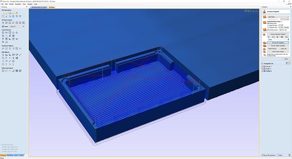
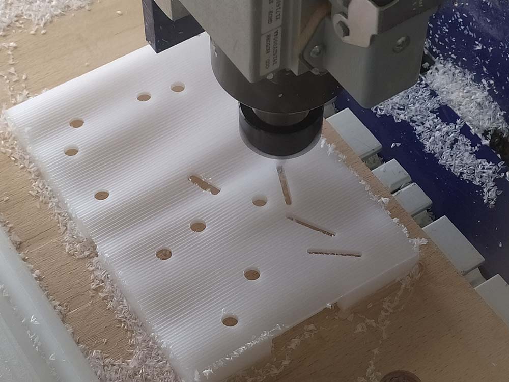
Experiment No. 17.5: CNC’d HDPE Enclosure¶

Experiment No. 18: 74LS04 logic amp¶
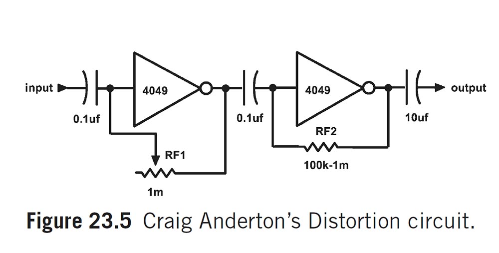
From Hardware hacking, here is the circuit I’m testing designed by Craig Anderton :
First I’m testing the simple pre-amp with variable gain from Hardware hacking:
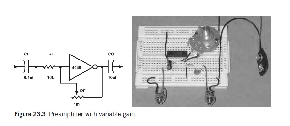
I am using the 74LS04 ubstead of the 4049. From what I understand the only difference is that the 4000 series can handle higher voltages but is slower than the 74*. But it’s not amplifying as expected. I think it’s because the 74LS04 is not UB (unbuffered) as mentioned in the Hackaday Logic Noise series.
I can still squeeze a bit of amplification with a 10K before the input and a variable 44K on the feedback loop but it’s mega distorted:
I switched for a 74HCT04 and the noise was fixed but it was not amplifying, it was slightly attenuating in fact.
Experiment No. 18: 74LS14 logic oscillator¶
Trying this oscillator with 74LS14 which has Schmitt Triggers:
With the LS I had a range from 1/50us to 1/800us and a lot of dead space. I switched the LS for an HCT which I had read had less good noise isolate (muhaha!) and get much more range (1/50us to 1/2ms).
Onscreen:

The triangle wave is super low voltage though and barely puts an image on the screen.
The sine is not great either, but I guess they could both be amplified? *EDIT not sure but it may be messing with the square oscillations.
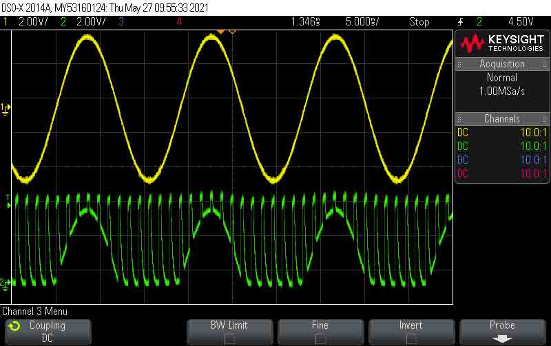
Connecting two oscillators together with a diode to make a sync oscillator as described here https://hackaday.com/2015/02/04/logic-noise-sweet-sweet-oscillator-sounds/ :
Gave some nice waves:
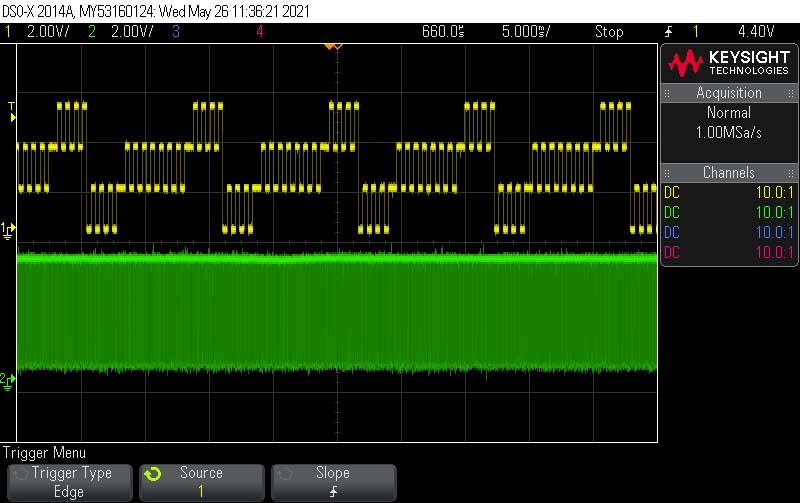
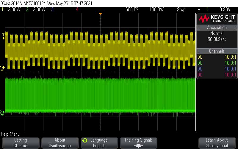
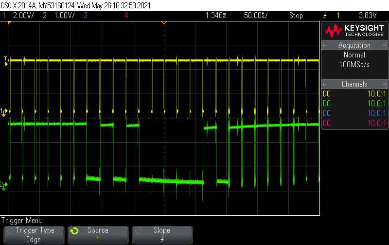
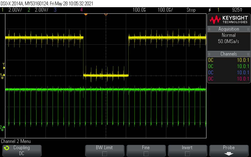
Experiment No. 19: 74LS420 binary counter¶
Forgot to pull out the CLK pin of the binary counter, and trkie the RESET low, and don’t use a female header because the rest are male ! Also, it’s soldered upside down which is annoying.
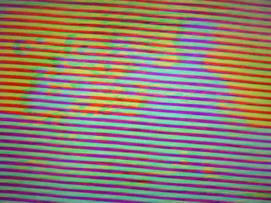
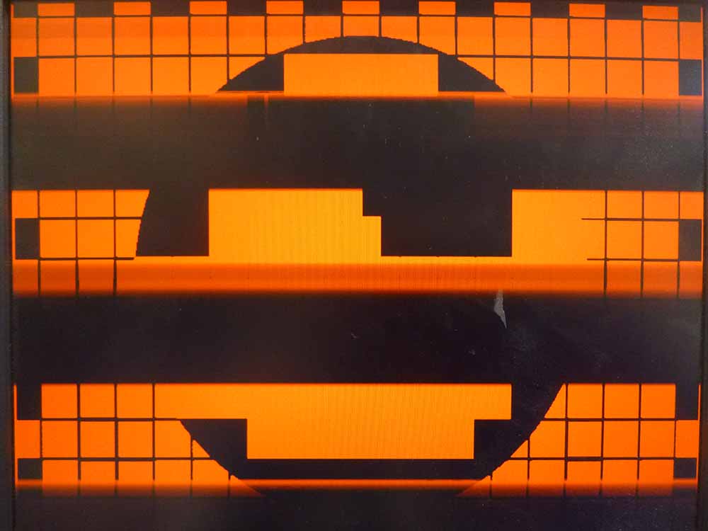
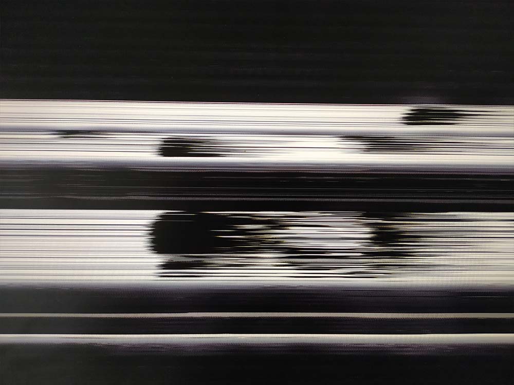
So far I’m getting a lot of horizontal lines…wondering if I can go further than this with these circuits.
From Logic Noise, I tried this circuit:
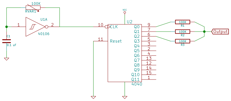
This works great and gives more diverse patterns on screen than the other circuits so far. It is super fun to change the pins and see the effect on the screen. I removed the 100K resistors to get this to appear on the screen however. I also used H-sync instead of the oscillator out.

With the clock to the binary counter floating and held in my hand I got some really nice patterns:

Involving the human body in the circuit is a nice way to get some analog in.
Experiment No. 20: R-2R DAC¶
This produces really nice output on the oscilloscope but nothing when plugged in to the VGA. I’m guessing I need to put it through an op-amp before sending it to the output. EDIT This appears to work.
Experiment No. 20: Shift Register¶
Here I’m going off on my own experiment, a PISO shift register that will hopefully take a series of crazy signals and output one color chanel.
Here I am feeding it output from the binary counter clocked and loaded with an oscillator and a synched oscillator respectively.
Looking good on the ‘scope but too weak to output any colors. I’m going to run it through a op-amp follower. EDIT This appears to work.
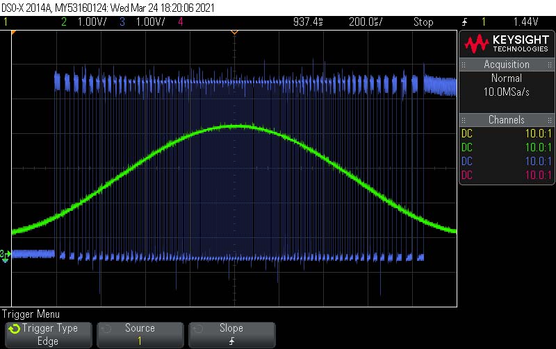
Experiment No. 21: Sample and Hold (again)¶
I forgot the capacitor! Also can’t get it to work with the LM358 (previously used the rail-to-rail MCP6241). Hmm. Ahh, I had the MOSFET connected backwards ! A little too hard to hack this one so it will wait for rev. 3.
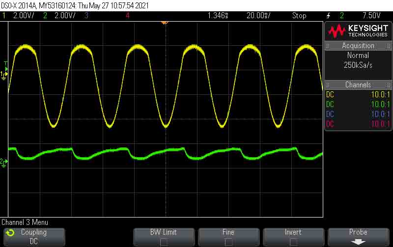
Experiment No. 22: VCA¶
Looking good:
Makes soft waves on the screen.
Experiment No. 22: LED - LDR¶
Only works for low frequencies (sub 100Hz) so not sure how interesting for this V synth:
Experiment No. 23: 4051 Analog Mux¶
This looks promising. I’m using the Z output directly to the color channel of the VGA and connecting output from the binary counter for the inputs and the 3 input selection pins.
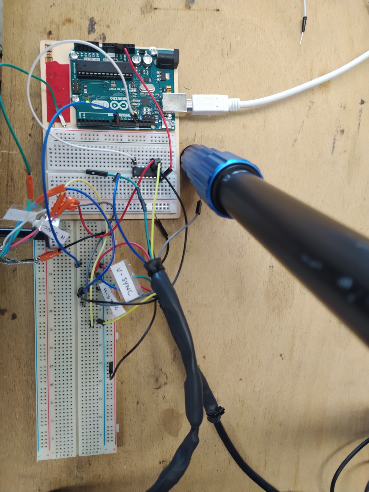
Experiment No. 24: Attiny85 v and h sync gen¶
This is working fine (a bit noisy but) in terms of signals but my screen doesn’t like it. I also tried pluggin in faster pixel signals with slower syncs and my screen complained of analog input :(.
Considering making a very simple VGA sync generation circuit from logic gates here:
https://hackaday.io/project/9782-nes-zapper-video-synth-theremin/log/32271-vga-sync-generation
EDIT I revisited making my own H and V sync signals.
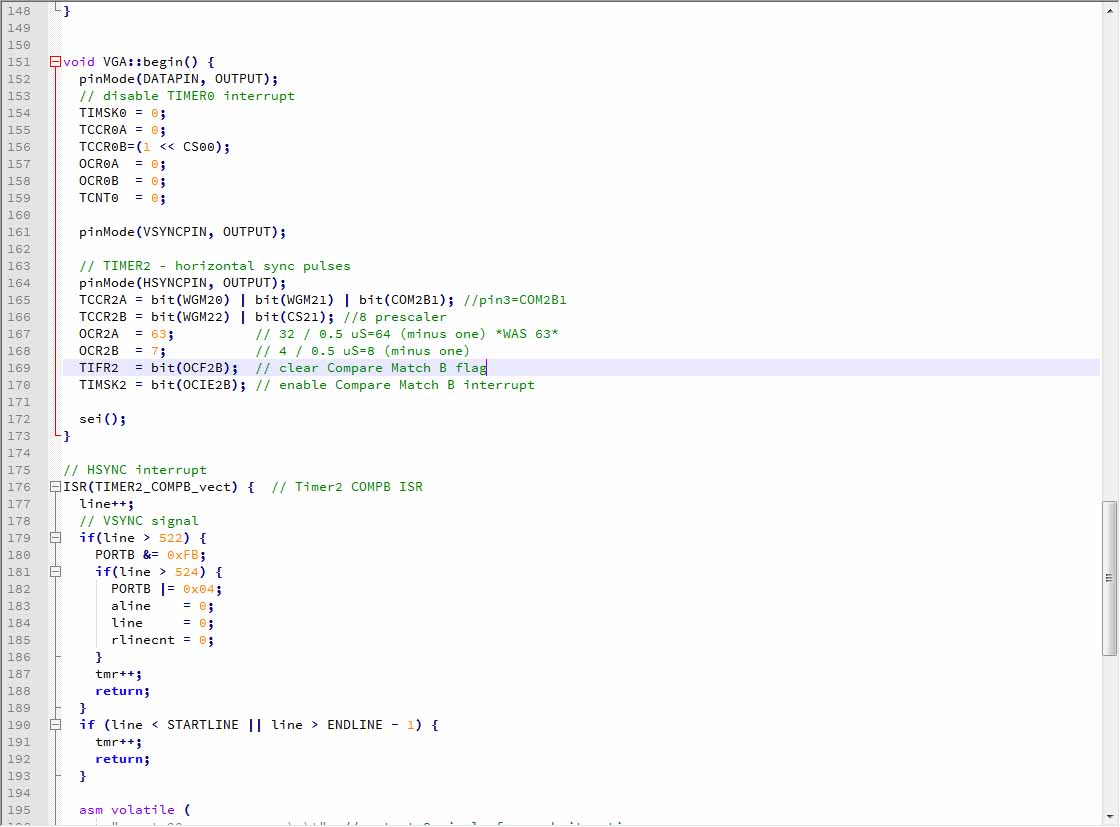
Following this tutorial: https://scanlines.xyz/t/tutorials-for-generating-video-sync-signals-with-arduino/104 I had H sync working fine but no V sync being generated. After hours of trying to figure out why, I discovered that the interrupt routine was not working to change the state of V sync. After trying different things I discovered that the ISR could only toggle pins, and no other way of setting the pins appeared to work for some strange reason. So I tweaked the code to just toggle pins and now it functions with resistors in place (with out the 68 ohm resistors my screen complains of unusable analog input).
I then added, thanks to Make: AVR Programming, Timer0 as well as a kind of pixel clock that is useful to drive ICs on the 0c74 that are SYNCHRONIZED with the H and V sync.
#define LINE_CYCLES 508
#define HSYNC_CYLCLES 60
#define VSYNC_LINES 2
#define FRAME_LINES 525
#define PIXEL_FREQ 1


volatile int linecount;

void setup(){
  pinMode(7, OUTPUT); // VSync
  pinMode(9, OUTPUT); // HSync
  pinMode(6, OUTPUT); // Pixel frequency

  //inverted fast pwm mode on timer 1
  TCCR1A = _BV(COM1A1) | _BV(COM1A0) | _BV(WGM11);
  TCCR1B = _BV(WGM13) | _BV(WGM12) | _BV(CS10);

  ICR1 = LINE_CYCLES; // Overflow at Cycles per line
  OCR1A = HSYNC_CYLCLES; // Compare high after HSync cycles

   //timer 0 in CTC mode
   TCCR0A = _BV(COM0A0) | _BV(WGM01) ; // Toggle pin on each cycle, no CPU clock prescaling/
   TCCR0B = _BV(CS00); // no clock prescaling
   OCR0A = PIXEL_FREQ; // go super fast


  TIMSK1 = _BV(TOIE1); // Enable timer overflow interrupt
}

ISR(TIMER1_OVF_vect)
{

 if (linecount == 0)          PORTD = PORTD ^ 0x80;    //Toggle the most significant bit of port D.;
 else if (linecount == 2)     PORTD = PORTD ^ 0x80;    //Toggle the most significant bit of port D.;
 else if (linecount == 3)     PORTD = PORTD ^ 0x80;    //Toggle the most significant bit of port D.;
 else if (linecount == FRAME_LINES) linecount = 0;
 linecount++;
}

void loop(){}
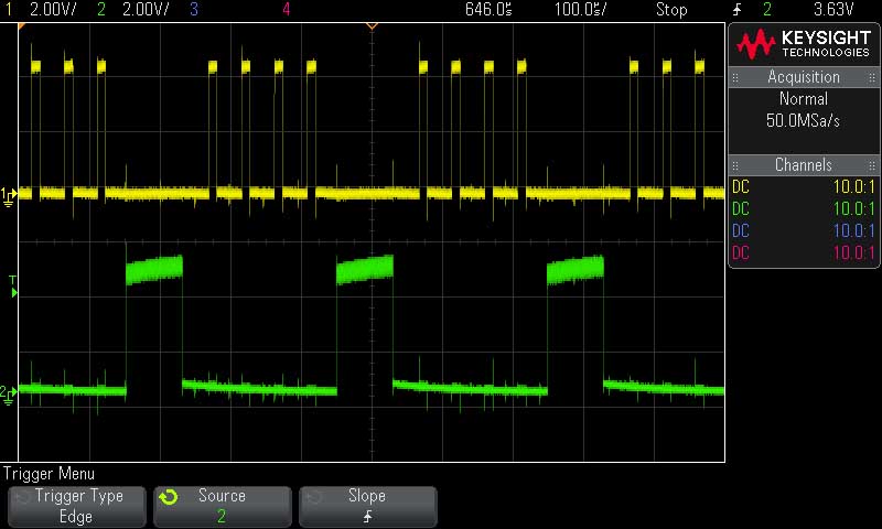
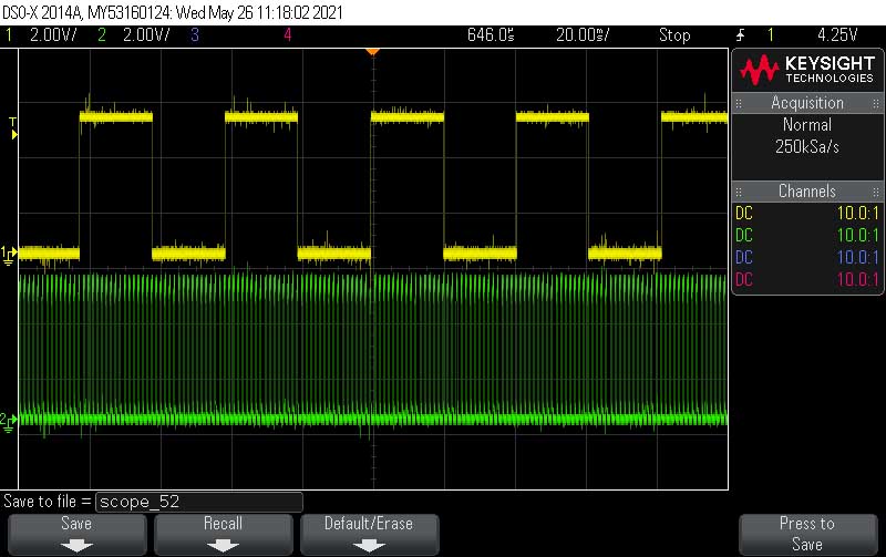
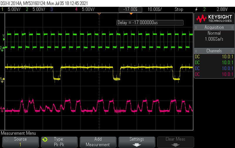
Here’s what it looks like on the ‘scope. Green is my new synchronized pixel frequency, yellow is H sync and blue is V sync :
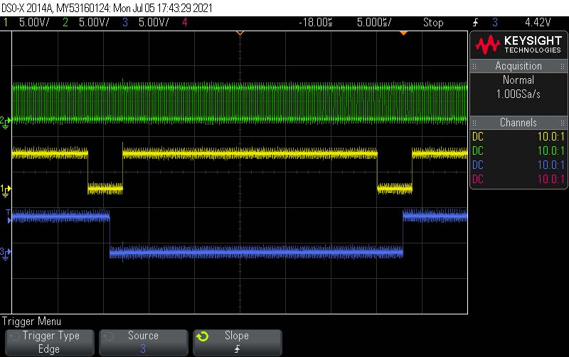
…and using the “pixel frequency” I’m generating as input to various modules on the oc74. Here green is my pixel frequency, yellow is H sync and red is the signal output from the oc74 (bin counter and analog mux combo):
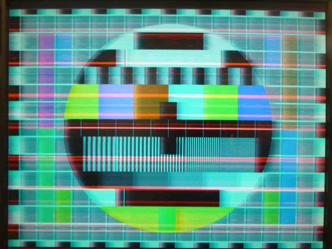
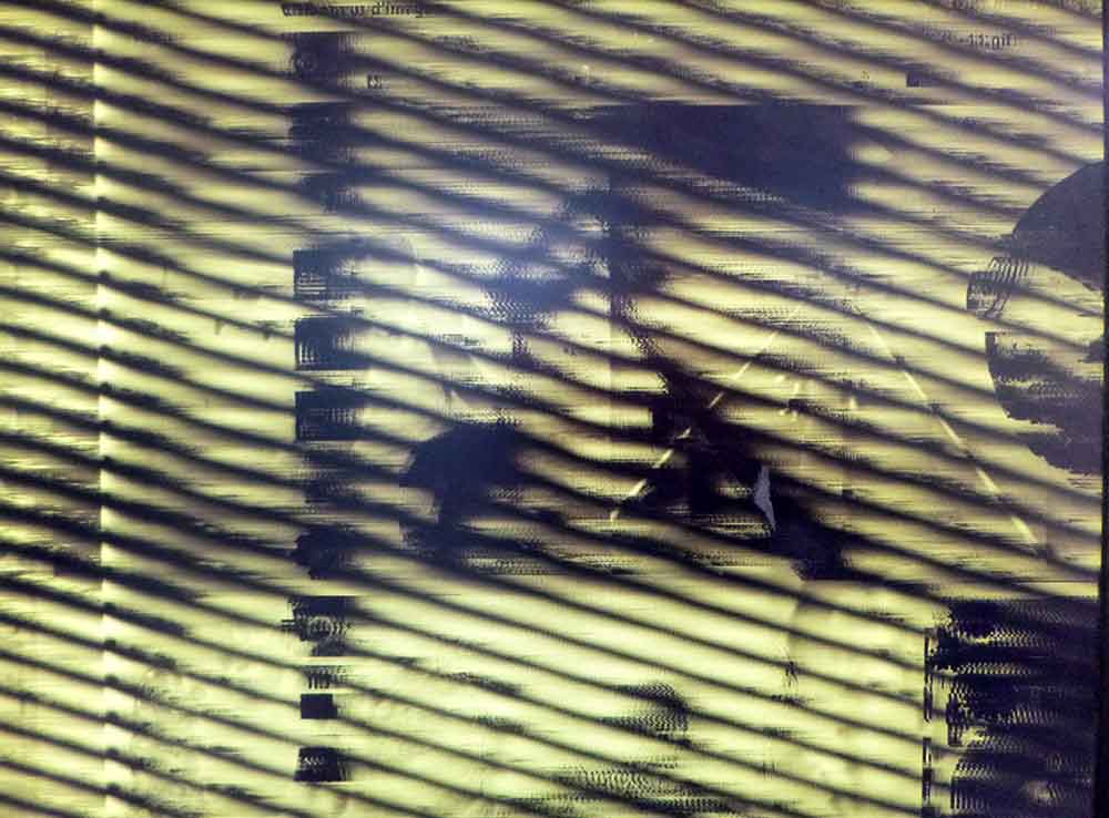
Experiment No. 25: VGA IN transformed with logic circuits to VGA OUT¶
Using the DAC to combine oscilators with color channels to B/W output you can just make out ghostly figures:
Feeding color channel information as clock for the binary counter, also throwing it in with oscillators at the resistor ladder before amplifying :
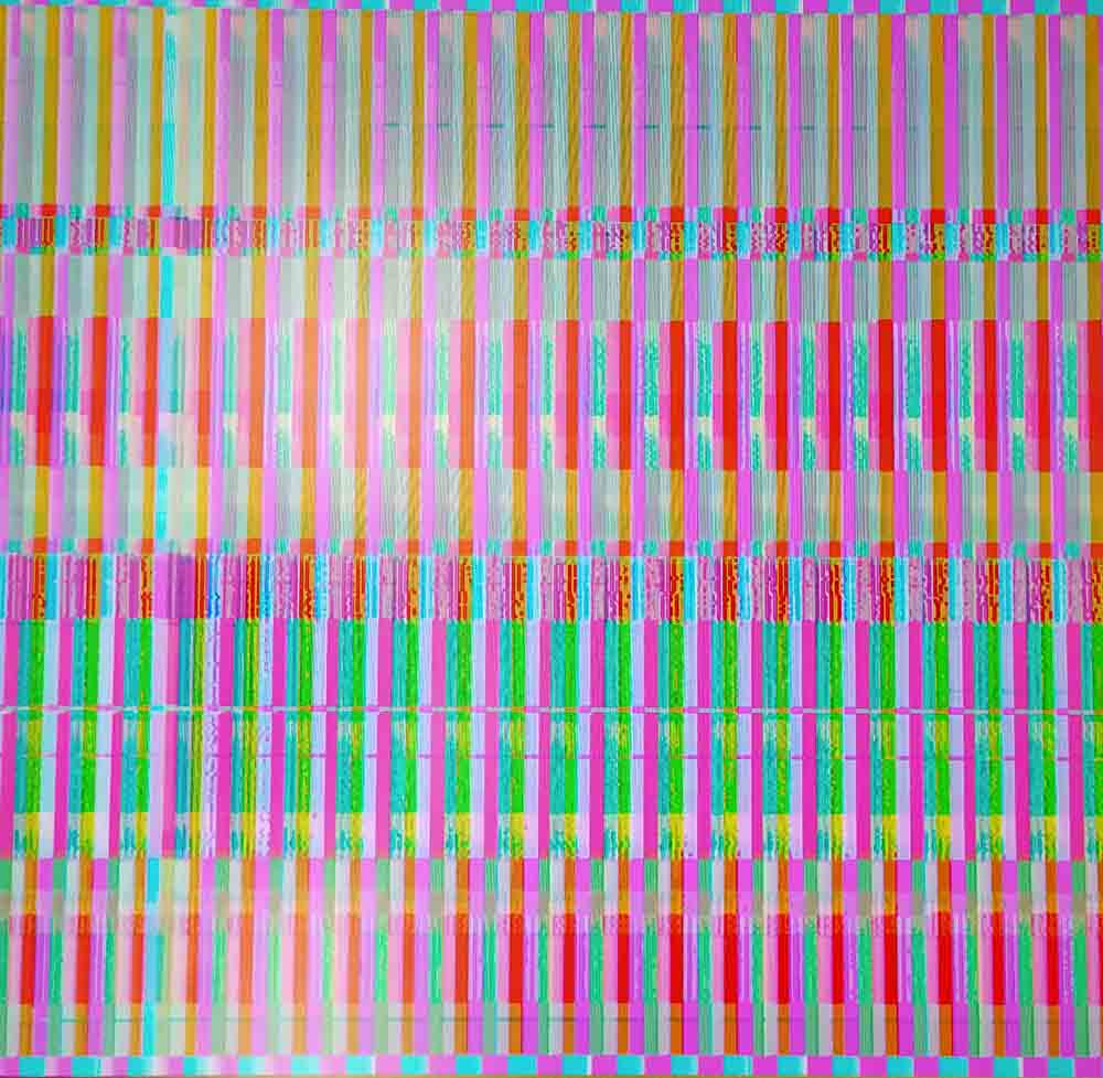
And here is a video I made from the output plus a circuit superimposed:
Experiment No. 26: Testing MAX frequency¶
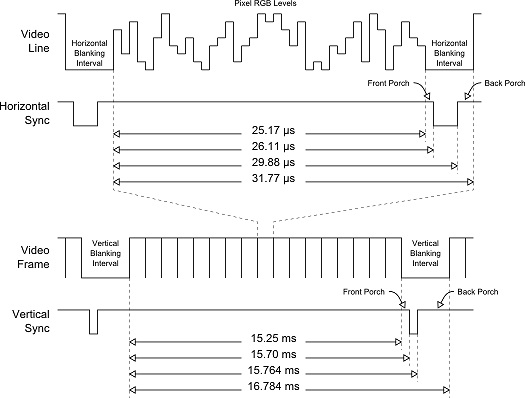
Checking out timing for VGA http://www.tinyvga.com/vga-timing, pixel frequency is in the MHz.
Looking at the HCMOS Design Considerations Manual
(https://www.ti.com/lit/an/scla007a/scla007a.pdf?ts=1622271047892&ref_url=https%253A%252F%252Fwww.google.com%252F),
we see that 74HC family can run at 40MHz.
I would love to be able to draw bit pixels like this cmos video synth by Psyingo (https://electro-music.com/forum/topic-53349.html) :
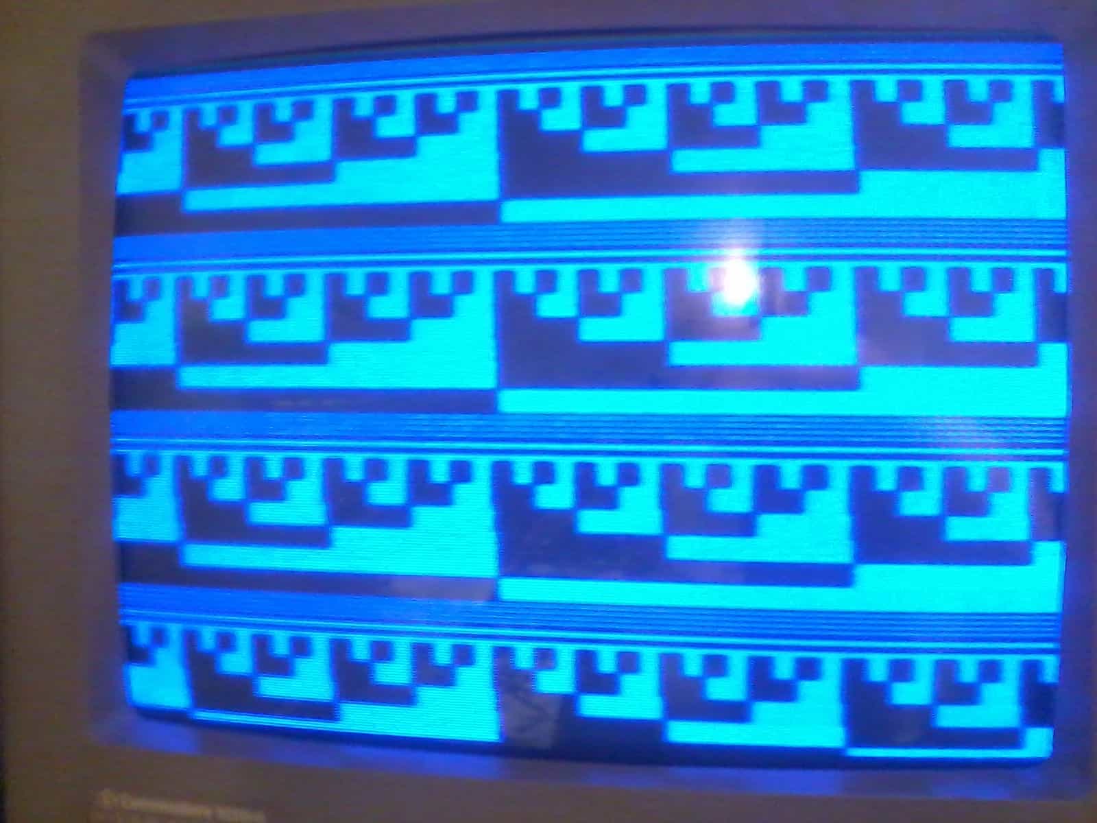
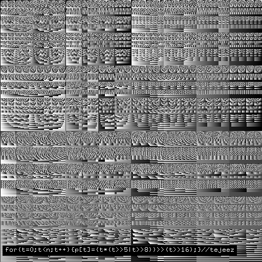
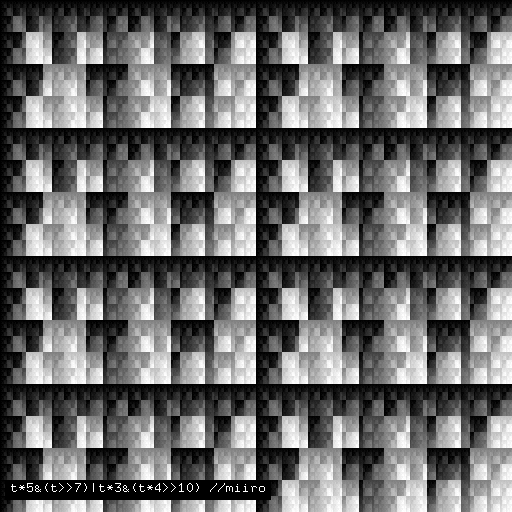
perhaps even to the level of this byte beat bitmap representation by Kyle MacDonald (https://www.flickr.com/photos/kylemcdonald/6197779509/in/album-72157627762378810/) ? :
My Abritrary Function Generator goes up only to 5Mhz, but I think I can see more grain in the output of the binary adder > DAC at that frequency :

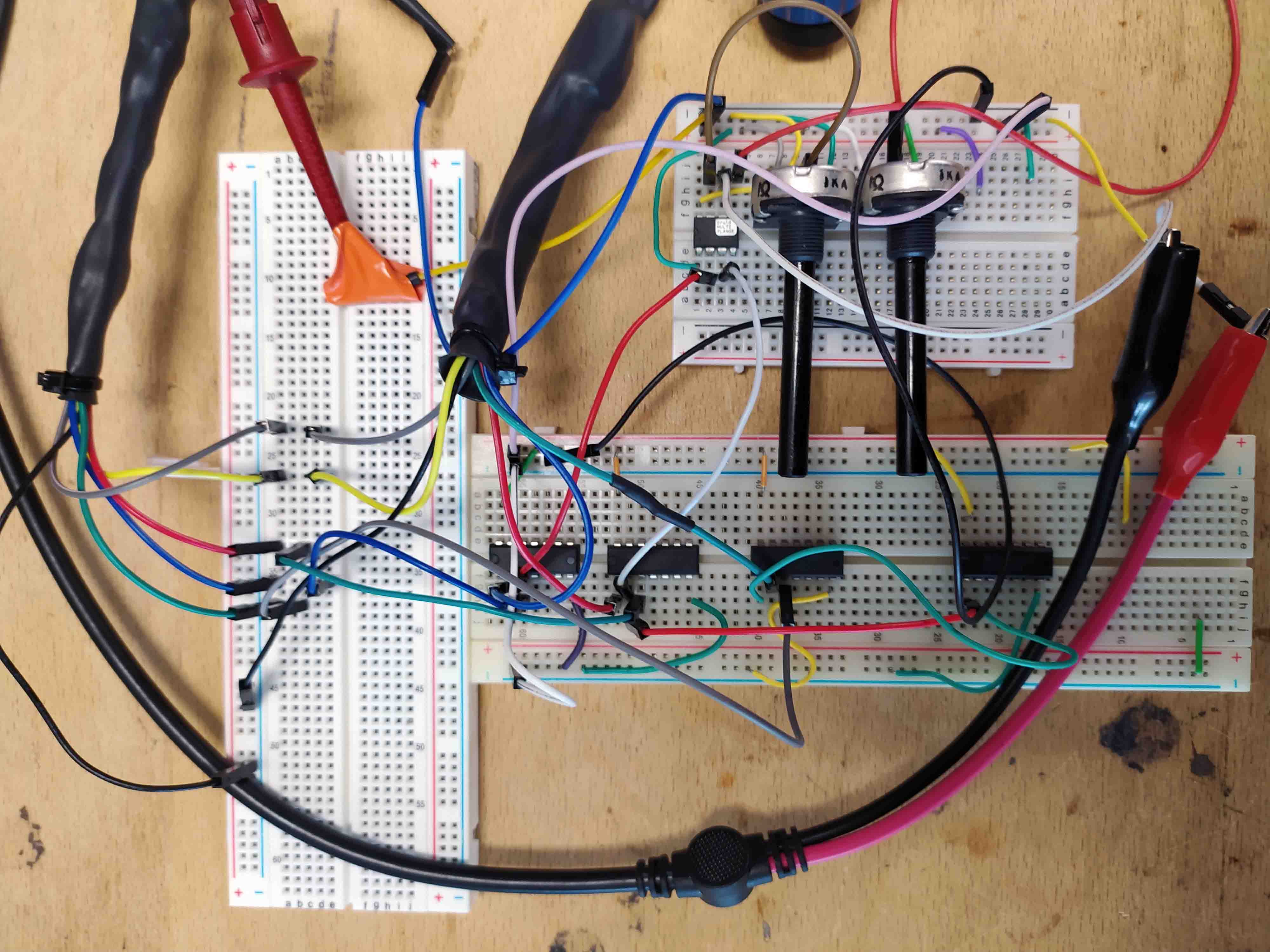
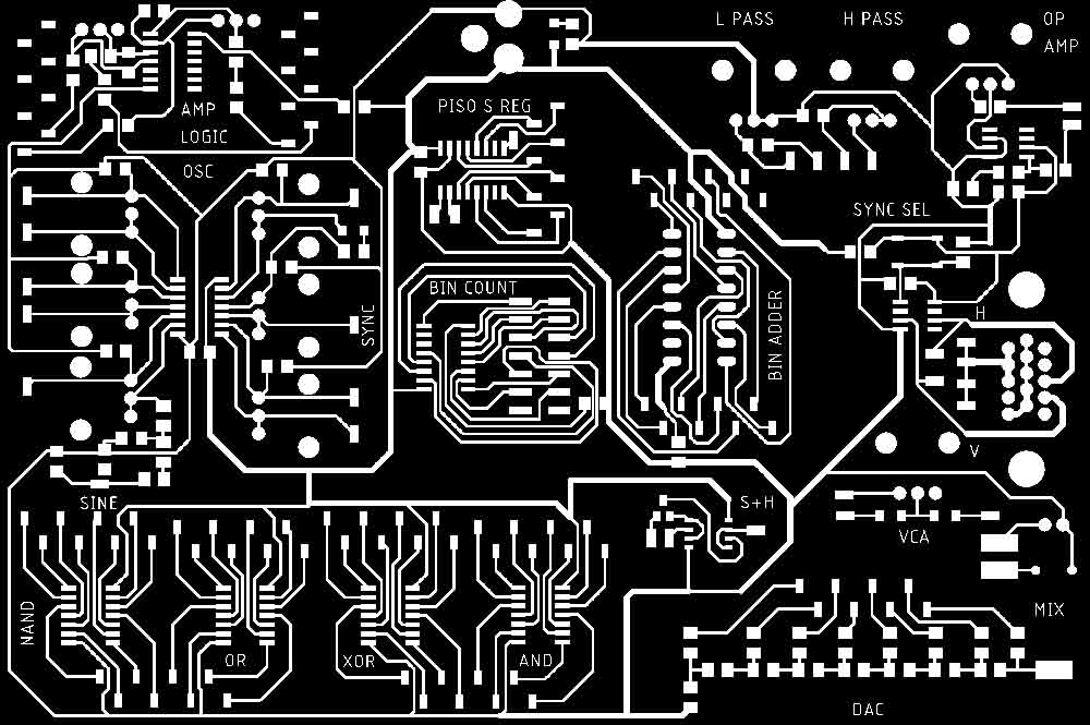
Experiment No. 27: Rev 3 of the board¶
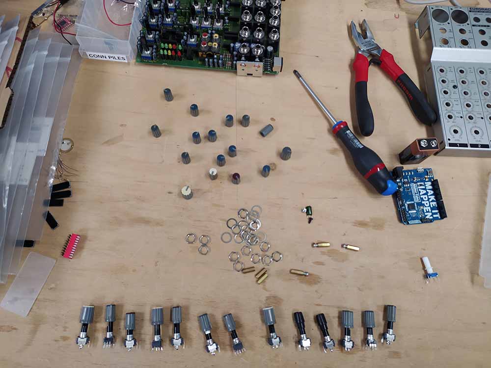
I have a diagrid set up, with around 20 different sub systems. I got my hands on a VCO that works in the 1MHz to 25MHz frequencies, as well as a decoder, a delay chip, NANDs with Schmitt trigger for gated oscillators, and SMD versions of chips I have only in DIP. I also switched to a different potentiometer which is SMD and 6mm in diameter.
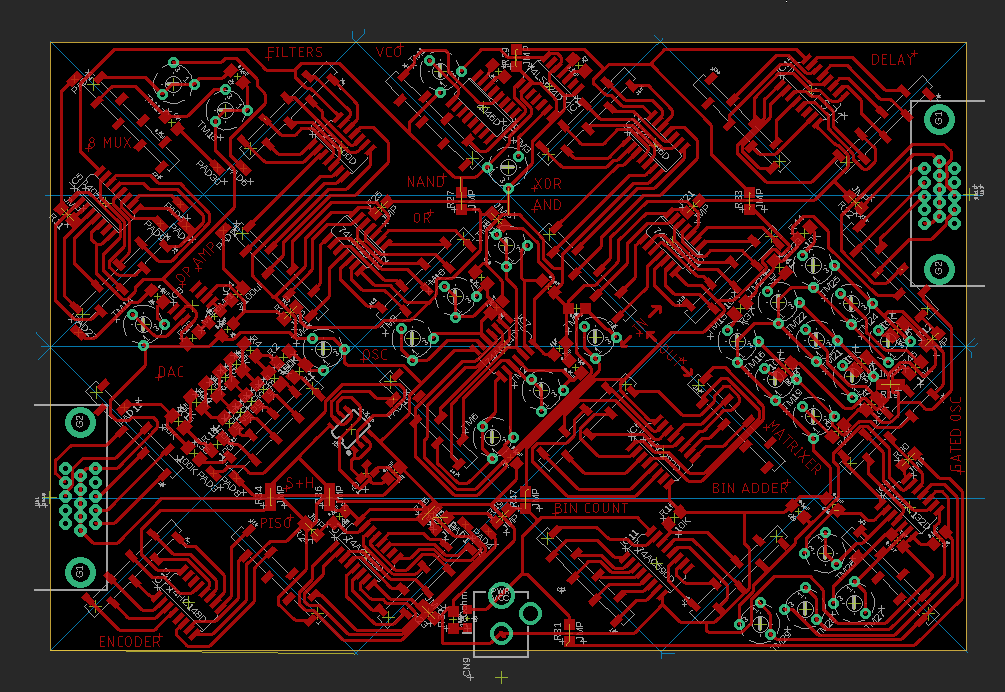
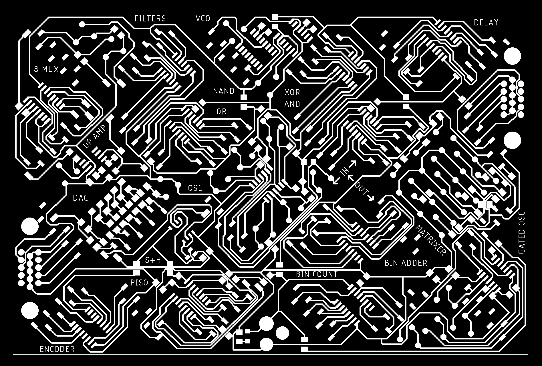
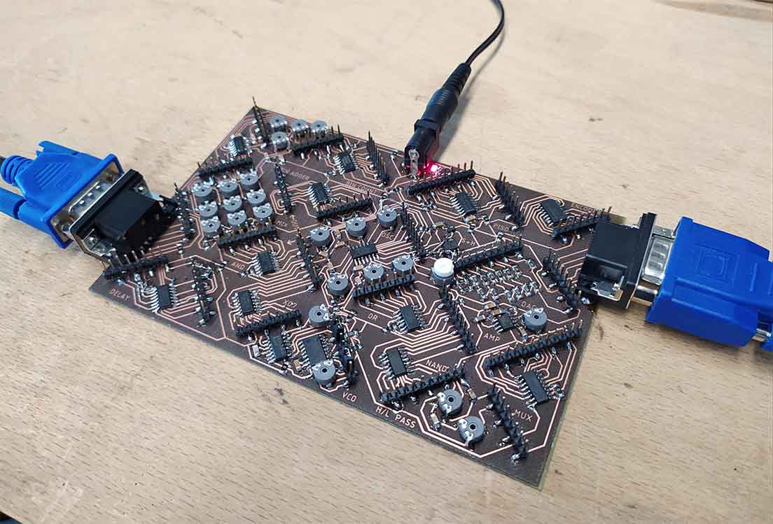
I have had to spend several days fixing errors and optimizing. Here it is ready to cut:
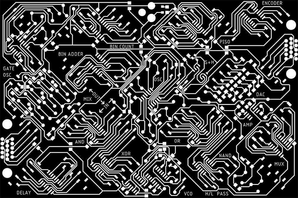
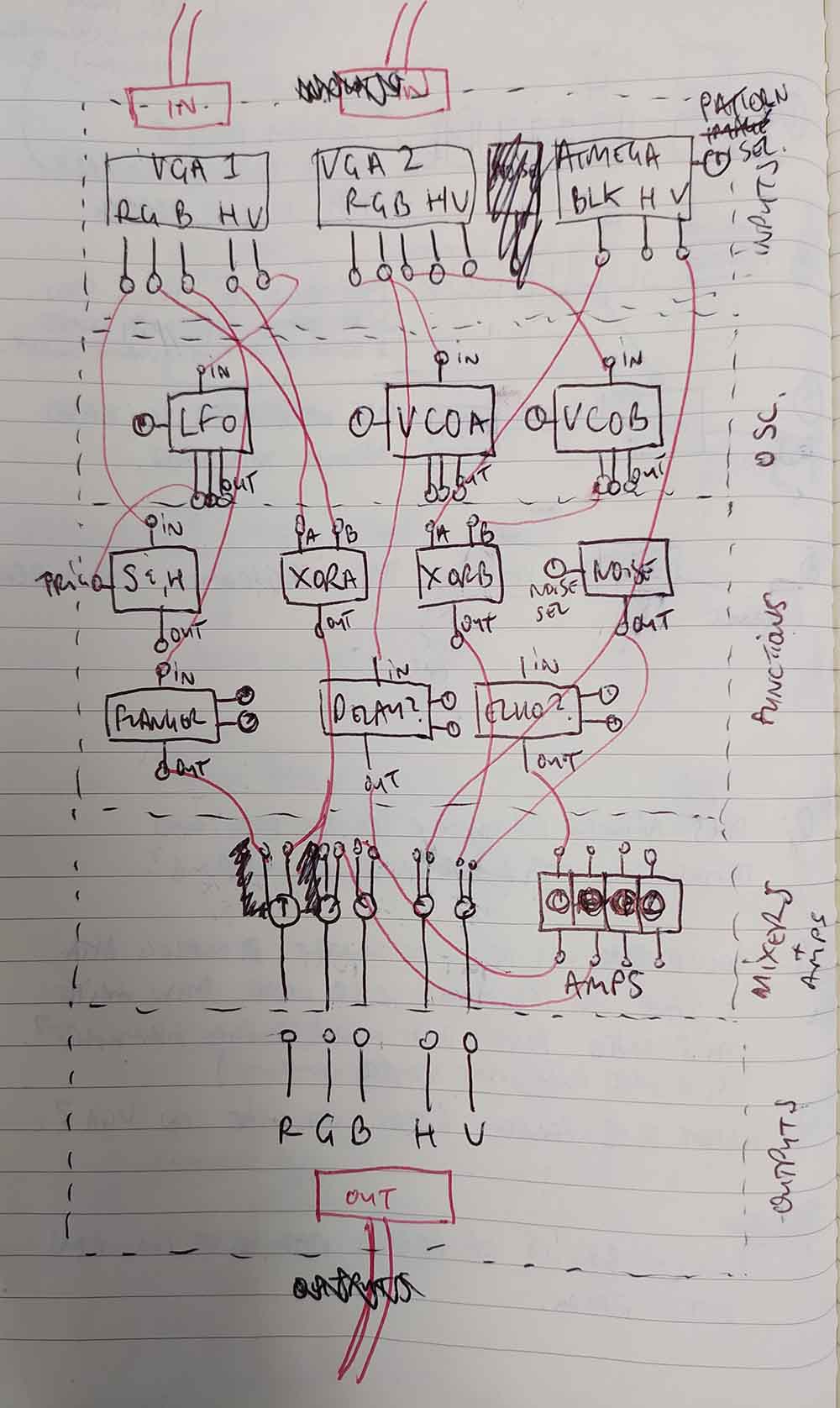
And here is a diagram of all the connections:
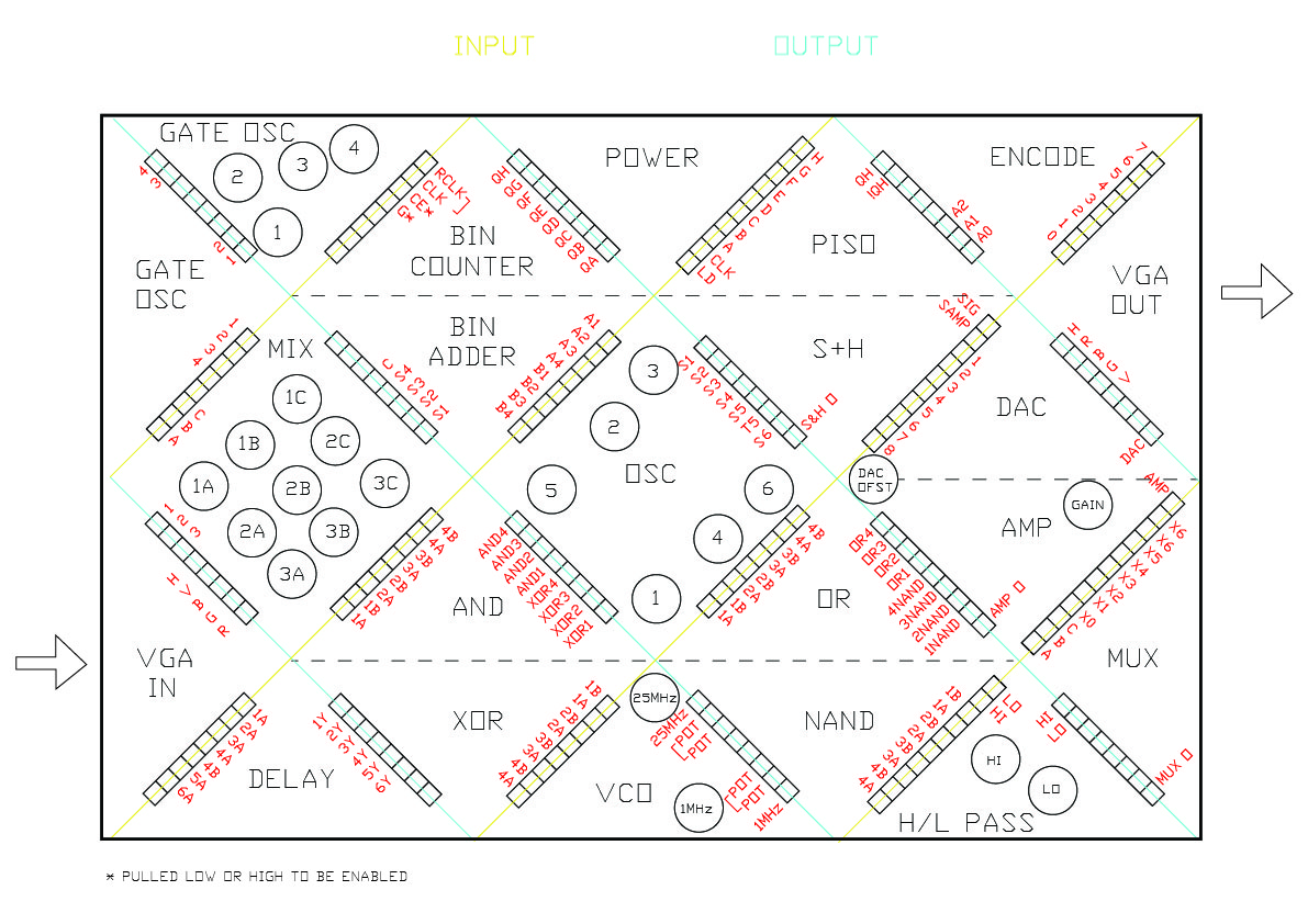
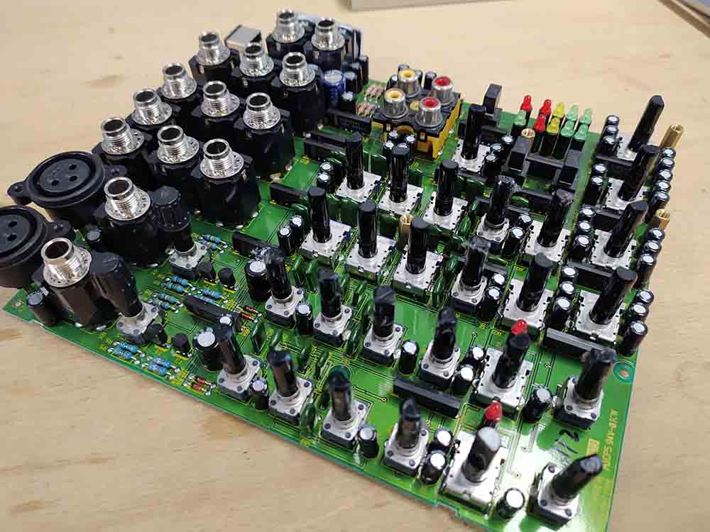
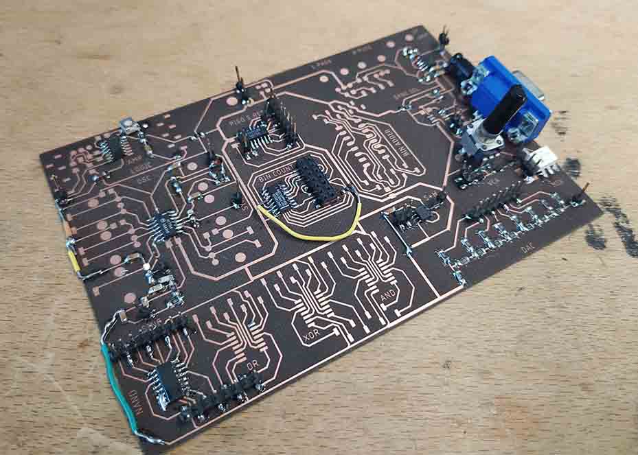
And assembled and plugged-in :
Errata:
-The delay chip sucks, I replaced it with the 4069UB which is way cooler. -I somehow managed to wire the sample and hold wrong. I hacked it to make it work inelegantly. -the gated oscillator is capricious, with 2.5 NAND gates working as expected…I tried to add a decoupling cap and it actually made things worse!
Fully assembled:
Experiment No. 28: Teaming up with VGAX library¶
Using VGAX to create the H and V sync and generating pixels using a simple pattern generating code (a barely altered code from their example called Pattern):
#include <VGAX.h>

VGAX vga;

void setup() {
  vga.begin();
  vga.clear(11);

}
void loop() {

for(int i=0; i<255; i++){
   for (int y=0; y!=VGAX_HEIGHT; y++) {
    for (int x=0; x!=VGAX_BWIDTH; x++) {
      if (x==0 || x==VGAX_BWIDTH-1)
        vga.putpixel(x, y, 3);
      else if (y==0 || y==VGAX_HEIGHT-1)
        vga.putpixel4(x, y, 0xf5);
      else
        vga.putpixel4(x, y, i%2 ? 25 : 150);
    }
  }
}
}
P.S. The line “i%2 ? 25 : 150” says that when i is even the two final pixels equal decimal 25, and when i is odd it equals 150.
I took the color signals and messed with them on the oc74 and spat out new signals:
EDIT
I also checked out what the signals sent by VGAX looked like:
Using the pixel signal from this code, along with the V and H sync, I could use it to clock the binary counter, mux etc. and all the pixels stayed put on the screen (instead of going diagonally off screen as usual when I take V and H sync from one place and generate my own signals). Clearly I need to syncronize the pixel clock with the V and H sync or I will never be able to put a pixel on the screen and keep it there…
I could make and program a little microchip circuit which just produces the syncs ALONG WITH a synchronized pixel frequency which I can then use for the oc74.
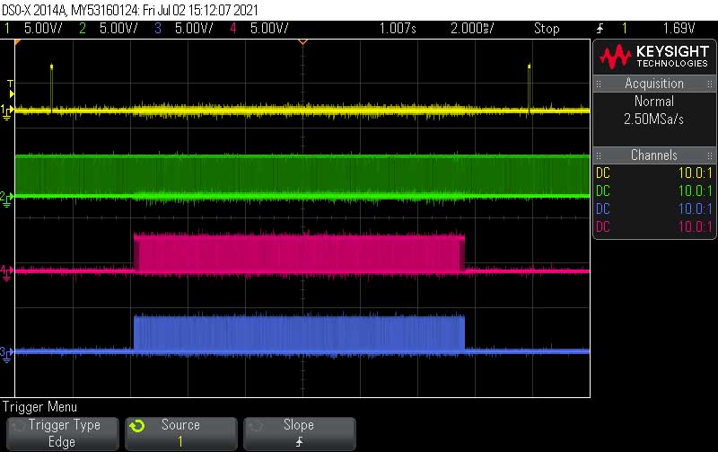
Experiment No. 29: Final Video (with synthesized sound!)¶
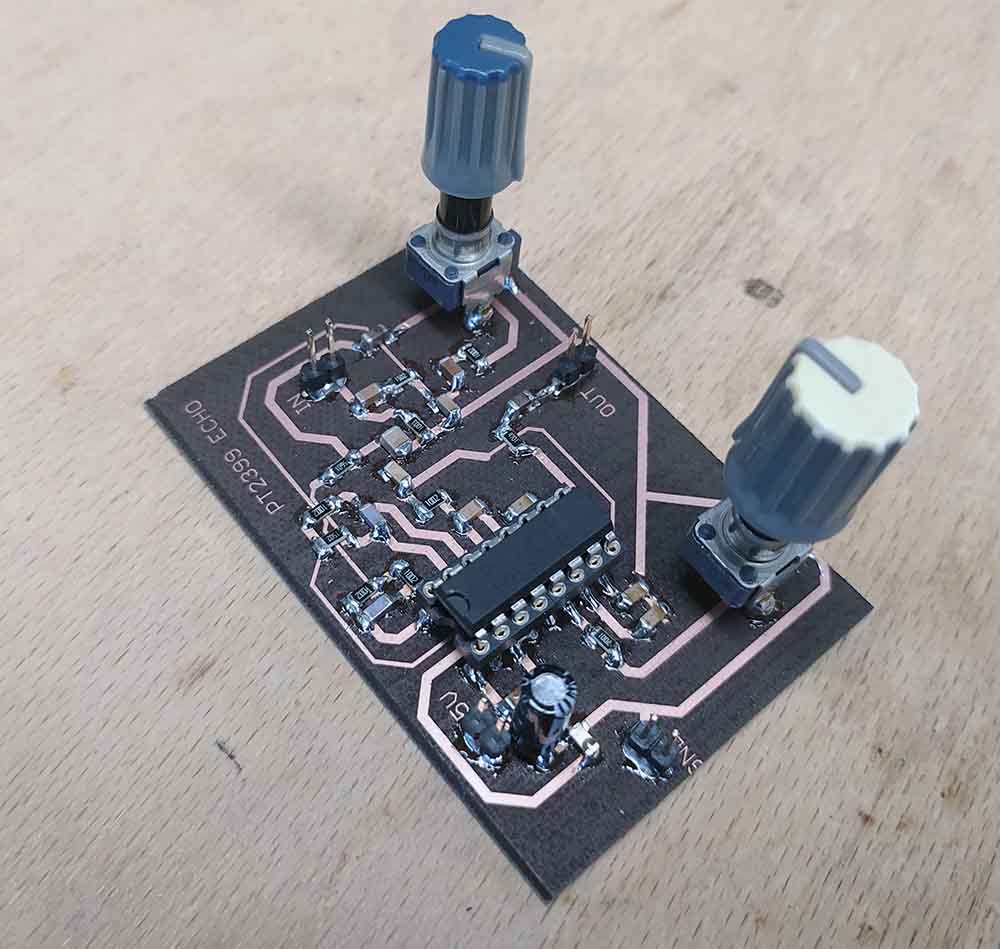
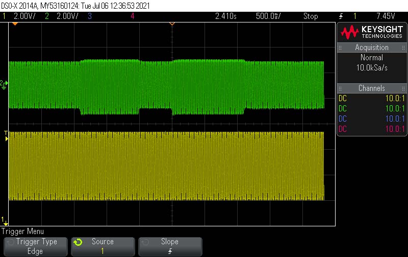
Experiment No. 30: Echo with the Princeton 2399¶
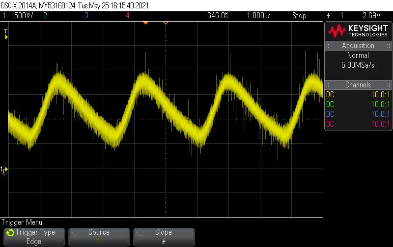
Using the famous delay chip the PT2399, check out the echo it performs on the ‘scope!

Doesn’t look like much on the screen - too slow…
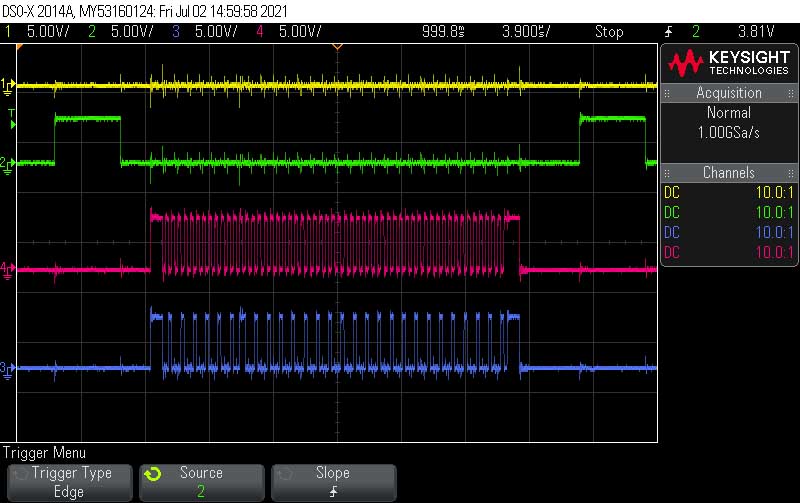
Experiment No. 31: ADSR with the AS 3310¶
Here is the board following the components suggested from the datasheet:
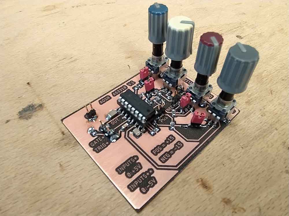
Check out how it performs on the ‘scope!
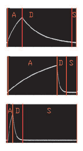
Here I’m using the trigger to show the Release:
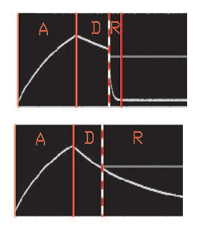
Doesn’t look like much on the screen - too slow…
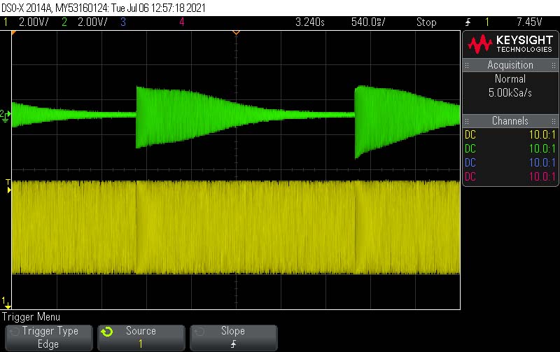
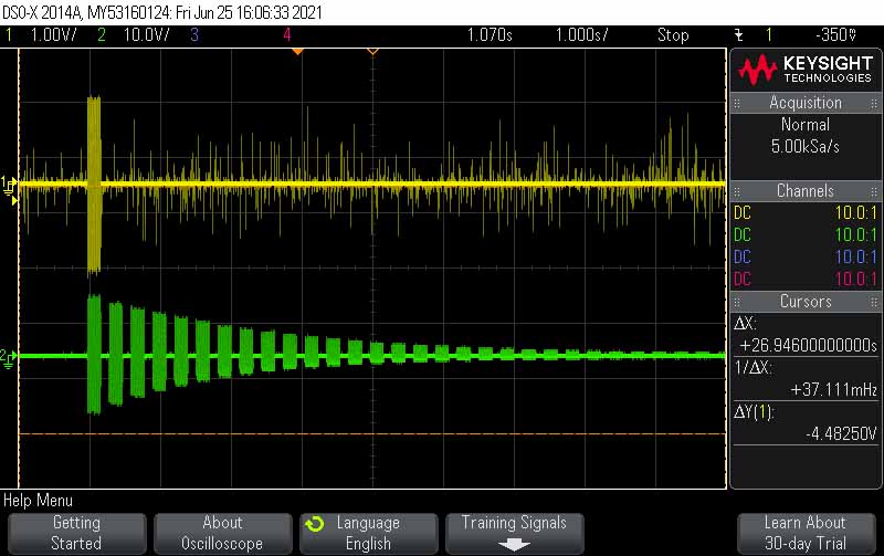
Experiment No. 32: VCF with the AS 3320¶
Here is the board following the components suggested from the datasheet:
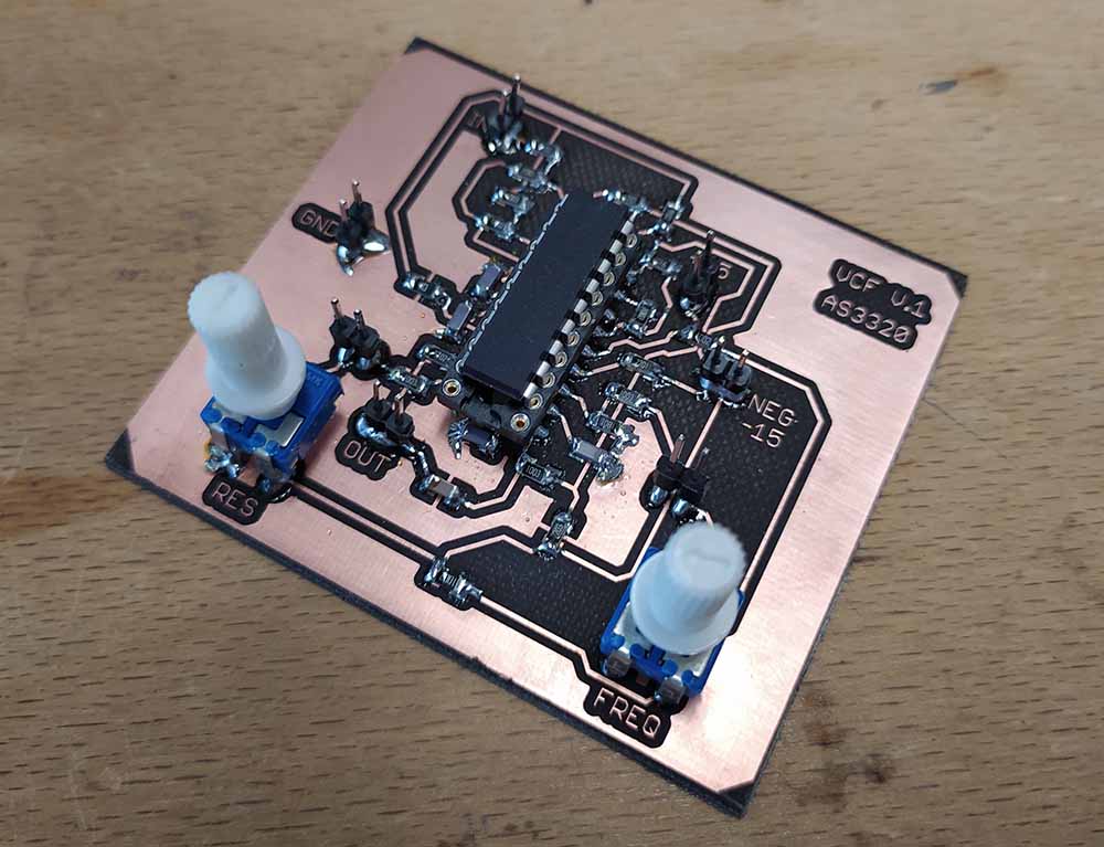
Check out how it performs on the old ‘scope! Here I am using the Arbitrary Function Generator in Sweep mode to show how the filter reacts at different frequencies.
Here is a log sweep:
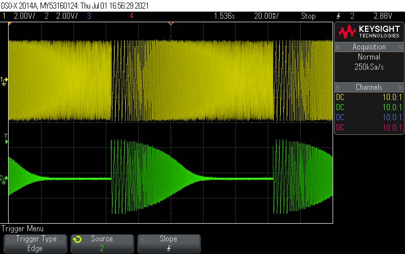
Here is a linear sweep:

I’m still trying to figure out the resonance control but here it is working a little bit at least using a 50K voltage divider and a 220K resistor before the resonance current input pin. Here I’m turning the knob from one extreme to the other and this accounts for the two hills.
In this frequency sweep, I’m turning the knob from one extreme to the other between two sweeps. This accounts for the taller edge on the second sweep response.