4. Electronics production
This week, we learned about the processes around milling and producing electronics. Our personal project was to make an in-circuit programmer by milling and stuffing the PCB and test it, and our group assignment was to characterize the design rules for your PCB production process.
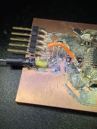
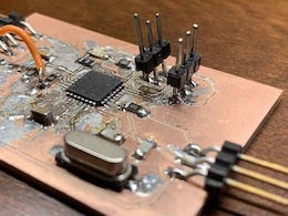
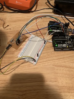
To start this week, we created a small board to blink an LED. This would show that our in-circuit programmer is functional once we create it. We used the ATtiny412 chip in the circuit with 4 other components and headers.
Hardware
Milling Process
To start the process, we milled out circuit boards using our lab’s PCB mills. I followed our labs workflow for the other mill:
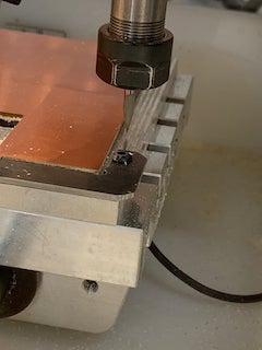
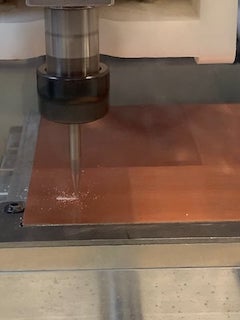
I started by uploading a file designed by our electronics instructor Dr. Adam Harris to the milling computer. I used the software Bantamtools to convert the board to a path and to control the machine. I then used two-sided tape to stick our board (one-sided copper) to the machine.
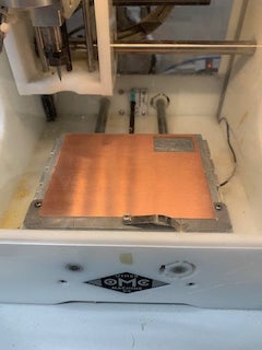
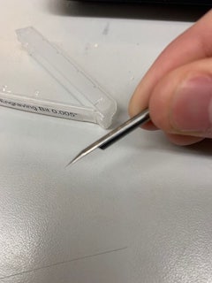
I then put the correct bit into the machine. To cut out traces, I used a 1/64” flat end bit or a .005” engraving bit. To cut out the board itself, I used a 1/32” flat end bit. After inserting the correct bit, I then used the machine’s automatic tool locator to determine the height of the bit through conductivity. I then determined the height of the copper plate by using the material thickness function in the machine. To do this, the machine uses conductivity through the bit to determine the height of the material, so I have to locate the bit first.
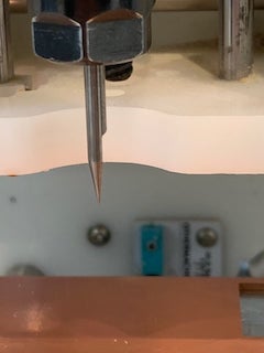
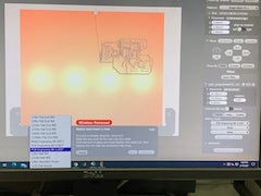
After determining the height of the tool and material, I could begin the milling process. I selected the trace option and clicked mill. For the .005” engraving bit, I first went into advanced settings and adjusted the trace depth to .25mm.
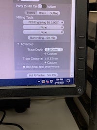
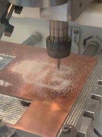
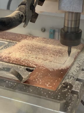
After cutting out the traces, I now cut out the board itself. I did this by changing the bit to the 1/32” flat end, and I went through the same setup procedure as before. I then unselected the traces option and selected the cut option. I then clicked mill again and watched the machine cut out the board.
I then washed the board with soap and water to remove harmful oils from its surface. I now had a completed board.
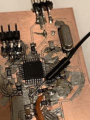
Now that I finished my board, I began to solder the components. I found the normal process of wetting the pad, soldering one end of a component, soldering the other, then adding solder to the original pad was very easy for me without the use of flux, so I used this process for the smaller components. However, for the larger chips, I had some trouble. I decided to try flux for the board and was able to solder it much quicker. I also found that using the angled tip on the soldering iron was helpful when soldering the chips. I think it is because I can reach around the individual pins, which made the process easier.
Later on, I used a strategy for soldering chips where I would solder one corner in place, then put a decent amount of solder on my iron and drag it across the pins fairly quickly until there were no bridges.
After finishing the board, I used an Arduino as a programmer to test it. I downloaded a program called JTAG2UPDI, which would allow us to use an Arduino Uno as a programmer, and a library for the ATTiny chip. However, my board would not burn. Actually, none of my classmates’ boards burned. Eventually, while on a very long phone call with our electronics instructor, we realized that when we downloaded a zip file from GitHub, it renamed itself with a -master. This tag would cause the program to not work. After removing the tag, most of my classmates were able to upload their code correctly. However, mine still wasn’t working. I used a multimeter to probe different spots on my chip and found that there was a short somewhere in my board. I checked the board under a microscope, and could not find the source of the problem. I re-soldered a few components that looked like they might be causing the problem, but they did not help anything. After about 30 minutes of probing and re-soldering, I opted to instead re-do the board.
I went through the entire process stated above again but was more careful on my soldering this time. Finally, when I finished my board, it was working and I was able to embed a simple blink program into the chip.
Programmer
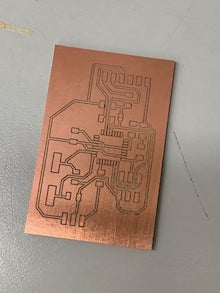
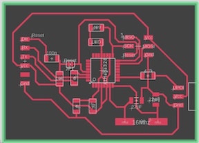
Now that I had a functional, programmable board, I could make the programmer and test it. I decided to make a UPDI programmer. I started by uploading the .brd file from this GitLab. I then milled out the board using the same process described above.
After milling the board, I went to solder the components. I started with the ATmega328 chip. I soldered most of the chip before realizing that I put the chip on backward. I tried to unsolder the chip but ended up ripping a trace.
I then re-milled the board and then proceeded to solder the entire chip backward - the same exact mistake. I angrily snapped the board in half after triple-checking it was wrong and re-milled for the third time.
After milling, I then soldered the chip the right way. I then started to solder the components. However, I eventually ripped a pad for one of the capacitors. I tried to make a solder bridge to repair it, but I only messed it up more. I took a picture of the failed board and restarted it.
Frustrated at the failed boards, I started to rush through the soldering process. The next attempt went even worse. I soldered the chip and a few components, but due to some error in the milling process, the traces did not turn out very well. I got a few of the small components down, but then ripped another pad. I had to restart for the fourth time.
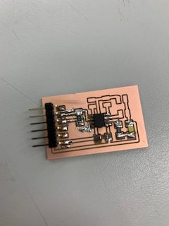
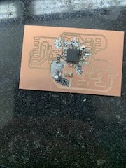
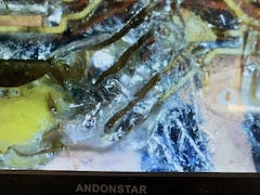
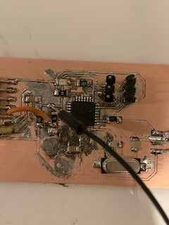
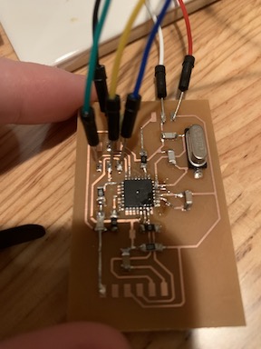
This time, the board milled out fairly well. I soldered almost every component but ran into some shorts around one of the header pins. I couldn’t figure out why there was a short, so I decided to remove the pin where the short was to look underneath it. However, the force from the pair of cutters I used to remove the header from the others completely ripped off its pad. I was tired of having to restart, so I decided to improvise. I cut off the end of a jumper cable and soldered it to a nearby trace. I then made a large solder bridge across some traces to where the header pin was supposed to go. I then used a razor blade under a microscope to cut the sides of the trace with the bridge. Finally, I soldered a wire between the trace that was cut so that it would still work. I was left with an ugly but hopefully functional board:
I then superglued the jumper in place and finished soldering the rest of the header pins to the board.
Software
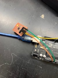
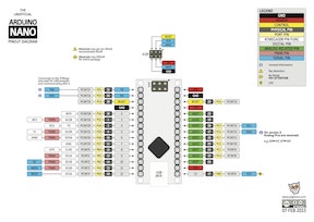
This programmer requires an external board to program it, then I can use the programmer to write to other boards. First, I looked at the pinout for the programmer board and for writing an Arduino nano from an Arduino UNO, since that requires the same pins. I then connected each pin in the programmer to the corresponding pin on the Arduino UNO.
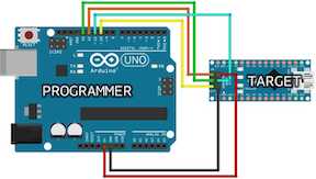
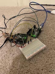
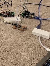
I wasn’t getting enough power, so I hooked up a second Arduino UNO and attached power and ground to a breadboard. I then made sure to add a common ground to the other Arduino, and hooked up power and ground from the breadboard to two of the three side header pins (the ground and power are flipped from the diagram).
I set my board to Arduino UNO, my port to the correct one, and my programmer as Arduino ISP (this was actually incorrect, which would cost me later). I uploaded the example “Arduino ISP” sketch, which came with Arduino IDE, to the Arduino Uno, and then uploaded a simple blink sketch to my connected programmer with the “Upload Using Programmer” option. However, it did not work, and gave me the error “could not find usbtiny device”.
At the time, I assumed this was due to a soldering problem, but it was actually because I selected “Arduino ISP” as my programmer instead of “Arduino as ISP”.
I probed my header pins with my multimeter and found that I had accidentally ripped one of the headers with the pad from the board when I was disconnecting the wires from the headers to take the board to my soldering station. I was very annoyed, but I had already made too many makeshift fixes to my board to let this stop me. I talked to my classmates and realized that I did not need this header for anything but flashing the programmer board. I followed the trace and found that it was connected to a jump that we had to solder to program the board, but had to unsolder once it was programmed to disable the reset of the programmer. So, I soldered a temporary jumper cable to the jump and went back to programming the board.
While in a call with my classmates while hooking up my board, I realized my mistake of using Arduino ISP instead of Arduino as ISP. I kicked myself mentally and tried uploading the software correctly. It compiled, and I almost thought it was working since my LED on my programmer flashed a few times. However, I was immediately hit with the following error message:
Yikes! Invalid device signature!
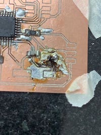
I told my classmates about it and was upset to hear that it meant that there was some problem somewhere in my board that was causing my board to fail. This error could be anything, from a bad component to a bridge, to a messed up chip. I used my multimeter to probe all over my board, and to my surprise, I could not find a single bridge. This was especially surprising because this is what my board looked like:
I then went through each component, one at a time, to measure to see if they had the correct value. However, I could not find a single messed-up component. This left only one source of the problem- my chip. Frustrated by the entire process of my board, I opted to restart from stage one instead of resoldering a different chip because my board was already really messed up, and I decided that if there was a problem other than my chip (which was possible- there could have been a short that I didn’t notice), it wouldn’t be worth the extra effort to find it.
So, the next day, I milled out another two boards and grabbed some components to take home to solder (I was only able to stay in the lab until 5 that day). I used a very high trace clearance to make it harder to solder bridges on my board.
After soldering the first board, I realized I forgot to bring header pins home, so I soldered some jumper cables to the pins I would use to flash the board and for power and ground. I then connected the correct pins to my Arduino and breadboard for power and flashed the board with a simple blink sketch, but I got the same error I got the same “invalid device signature” error.
I knew I had not made a bridge because I had a very large trace clearance and there were no connected pins on my 328 chip, even under a microscope. So I assumed I had a bad component, and I soldered the second board I milled out at school.
After soldering the board, I ripped header pins of a previously failed board I had at my house (because I had plenty of those lying around), and I flashed the board with the blink sketch.
At first I got an error, but I tried again and for some reason it blinked at 1/20th the speed it should have. I uploaded the code again, and IT WORKED! I took a quick video:
and then went to burn the bootloader so I could upload the JTAG2UPDI sketch to the programmer. And then - invalid device signature. I checked to see if I ripped a header pin pad, but I hadn’t. I didn’t think I would because I connected two headers between the Arduino and programmer so that I could disconnect pins without putting excessive force on the programmer header pins. I assumed I did something incorrectly on the software side. So, to double-check that I hadn’t messed it up, I re-uploaded the blink sketch.
This part especially confused me. I somehow got three different errors - “could not find USBTiny device,” “content mismatch,” “invalid device signature.” Disheartened and frustrated, I probed EVERYTHING with a multimeter. No shorts. I checked the value of each component. Everything was correct. I assumed I had a bad chip, which makes sense because of the weird 1/20 speed blink program.
So I tried to unsolder the chip to replace it with a different one, and on queue, I ripped a trace.
Back at square one, I re-milled at school the next day and restarted. I made the trace clearance to 0.5 mm to make it harder to bridge, but I made the mistake of forgetting to make multiple passes with the 1/32” bit instead of the .005” bit. This caused the board to mill out much more roughly, with many more copper threads along the edges of the traces. I continued on soldered the components anyways because I wanted to make this my last attempt. I got all the components soldered, and probed my board with the multimeter. I found a few shorts, mostly between parts of my chip and between nearby traces due to the poor quality cut. I talked to Dr. Harris about it, and he recommended that wash it with soap and a strong stream of water to try to remove some of these traces. While this method did clean up most of the board, I still had these shorts. I then pushed a cool soldering iron through the traces to clean them up and resoldered the pins, and I eventually removed the shorts.
UPDI Code Process
I then went through the whole process of uploading code to my board. This time, it was successful! I uploaded the blink sketch to my programmer, and it worked. I then burnt the bootloader on my board.
To upload the jtag2updi code, I first had to download the library and the attiny412 board. I downloaded the .zip for the JTAG2UPDI from the GitHub and opened the file into Arduino. I also downloaded the board for the ATTiny412 in Arduino/Preferences and adding the link for the megatinycore library:
http://drazzy.com/package_drazzy.com_index.json
I tried uploading the JTAG2UPDI code to the Arduino, but it didn’t work. After a long debugging process and phone call with our electronics instructor Dr. Adam Harris, we found that the problem was with the -master tag that is added after uncompressing a zip file. I removed the tag, uploaded the code, and it worked.
Many thanks to Adam Harris from Sheek Geek for helping us set up our UPDI programmers.
I uploaded the JTAG2UPDI program to the programmer. It compiled correctly, and so I cut the jumper cable “JP1” so that the board would not reset itself when uploading code, I attached the UPDI board to my programmer, and I connected my outputs from the programmer to the blinky board. I did not have my board at school, so I used my classmate Charles De Mey’s board. Finally, I attached a USB cable between my computer and UPDI, set my board for ATtiny412 (the chip on the blink board), and uploaded it through my programmer. And it worked! I quickly took a video before I inevitably ripped a pad, and breathed a sigh of relief.
The board I borrowed already had a blink sketch on it, so I uploaded one that would blink twice as fast:
That night, I set up my board to upload to my ATtiny chip to double check that they both worked, and it uploaded:
Reflection
I think the main reason I had so much trouble this week is that I was rushing. While discussing my work this week, our teacher Dr. Fagan told me about a Navy Seals saying: “slow is smooth, smooth is fast.” This applies to the way I was working this week - I definitely was rushing when I soldered the chip backward twice, and I think this was also one of the problems I had while soldering. I don’t think I put the amount of focus I should have into making sure I did not mess up a single connection, not carelessly ripping pads, etc. and I think if I had slowed down, I would have had a much less difficult time this week. I will definitely remember this struggle in future electronics weeks so that I do not waste components or time.
Group Project
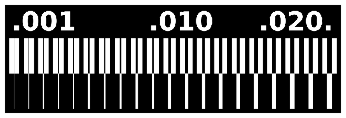
Our group assignment for this week was to “characterize the design rules for your PCB production process.” Our documentation for this week’s assignment can be found here.
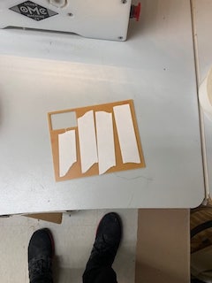
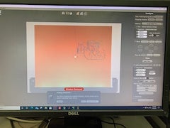
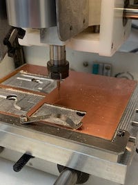
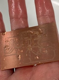
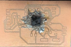
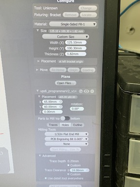
For this week’s assignment, we used Fab Modules to turn these two PNG images for background and traces into a .nc file. We did this by first uploading the images to Fab Modules under a .png format, then set the output format to .nc for the Bantamtool (previously known as othermill) mills that our lab has. Then we set the process to the 1/64” bit for the outline and the 1/32” bit for cutting through the board. Finally, we saved these files and opened them on the computer we would be milling on through the BantamTools software. We used the BantamTools software to control the CNC mills and cut out the board, and we ended up with this board:
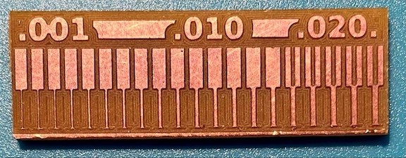
The board turned out fairly well, with the smallest trace of 0.001” turning out well, as well as a minimum trace clearance of 0.016” being cut.
This week’s files can all be found in this zip file.