Introduction.
In this week I met several software for electronic design, some paid and other free
software, the world of electronics is interesting from its design, going through the
component integration stage in design, using Ohms law to determine resistance .
The KiCad workflow consists of two main tasks: drawing the outline and drawing the board.
Both a library of
Components like a footprint library are required for these two tasks, the fablab library
must be downloaded for kicad.
It is incredible that I can customize my own circuit, due to lack of machinery, tools and
electronic components, it was not possible to produce my circuit. I am in the design phase.
I don't know much about how to integrate electronic components in a circuit or what the
position of a resistor or diode should be, for example, but that's why I'm here because it
makes me something so wonderful to be able to integrate the electronics part with the
programming.
Group assignment.
group project: use the test equipment in your lab to observe the operation of a microcontroller circuit board
I didn't do the group activity, because I don't have the milling machine, I also
don't have the electronic components to integrate the circuit, but as soon as I
have the components to solder the circuit, I will carry out the activity.
individual project
Redraw an echo
hello-world board,
add (at least) a button
and LED
(with current-limiting resistor) check the design rules, make it, and test it extra credit:
simulate its operation.
- I will use ATtiny45 hello.ftdi.45
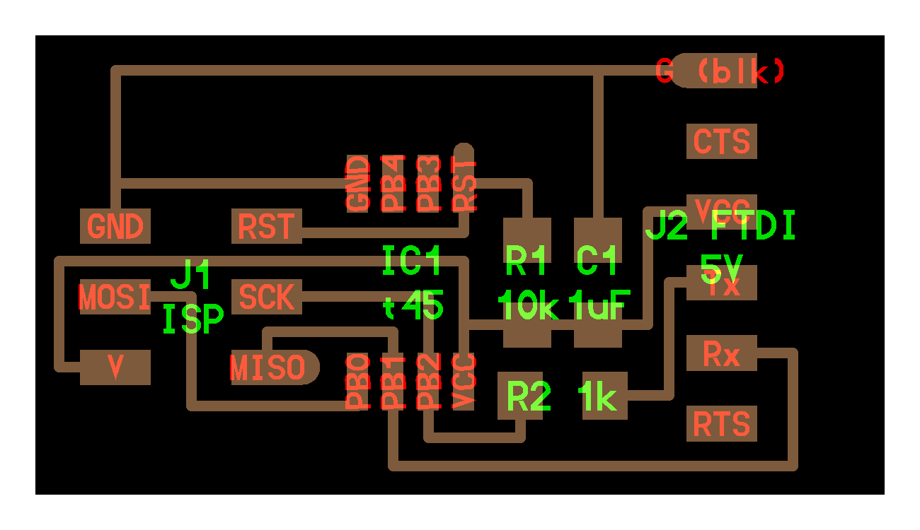
- It is necessary to include the library gitlab.fabcloud.org/pub/libraries/electronics
Components
| Name | Fab Library Symbol | |
|---|---|---|
| 1X 6-pin programming header | AVRISPSMD | |
| 1X 6-pin header | FTDI-SMD-HEADER | |
| 1X Microcontroller: attiny45 | ATTINY45V-10SU | |
| 1 Resistor 10 k | SMD-5X3MM | |
| 2 Resistor 500 | SMD-5X3MM | |
| 1 Resistor 1k | SMD-5X3MM | |
| 1X Button : (OMRON switch) | 6MM_SWITCH6MM_SWITCH | |
| 1X 1uf capacitor | C1206FAB | |
| 1X LED | LED1206 | |
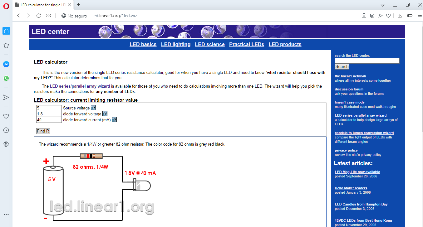
It is necessary to calculate the current limiting resistance for the LED so that it
does
not burn. For this, the values of the Led data sheet are required, Ohmn's law must
be
applied to know the workload, to use the calculation I used an online calculator
To perform the redesign I use Eagle.
A schematic diagram in circuit design is a drawing that represents a circuit, using symbols
to represent the actual electronic components. The most basic symbol is a conductor (a
track) that is represented as a line. If the lines are connected in a diagram, this is
represented by placing a point at the intersection.
How does Eagle work?
It has 2 ways of working.
Graphical Icon Toolbar: You can use the icons on the left toolbar, hover your mouse over
them to see what they do. (enabled by default).
The list of command line commands listed below also applies to icons.
ERC and DRC are found under "tools" in the top menu.
Command line: You can start typing a command at any point, then select the item on the
schematic / board that you want to interact with, see the command section below.
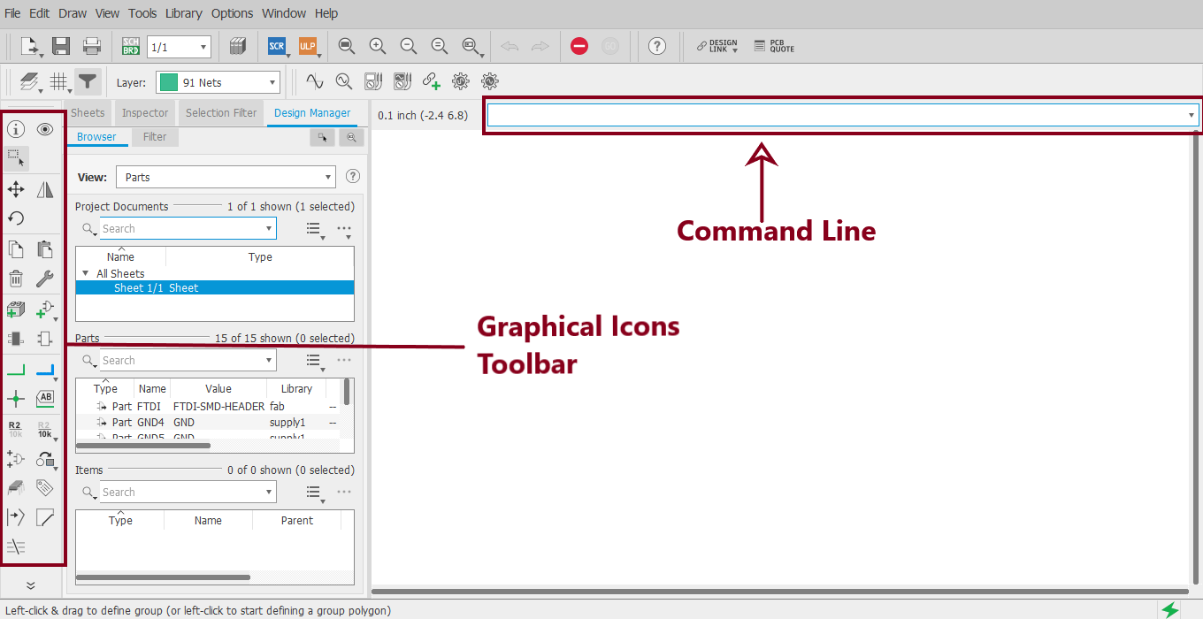
Eagle has a command line (just start typing commands) - basic commands include:
- add = opens up the libraries so that you can add components in Schematic view
- move = moves an item
- net = makes a logical connection
- junction = adds a junction
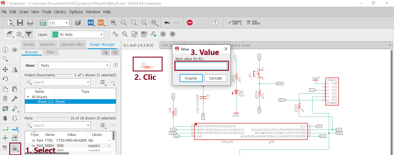
- value = addes value to components (i.e. ohm rating)
- name = names a component
- label = displays the name of a component in schematic view
- copy = copies an existing component on the schematic.
- route = used in Layout view, this tells you if you need to add a connection (follow yellow lines)
- ERC = electronic rules check; this ensures your board will actually work (use in schematic view)
- DRC = design rules check (in board view) - keep all the default settings (16 mil is fine); it should display a "no error" message in the bottom left hand corner of the screen
- group = groups components in Layout view together; if you right-click, then you can choose Move: Group to move the grouping
- rats = in board view, tells you if you have airwires
- rip = deletes connections in layout
- show = after typing this, select a component to see information about it displayed in the bottom left corner of the screen. Also, if you type show + [name of component] you can see that component highlighted. You can use this to see all the ground traces, for example.
- text = allows you to add text to your board. You can also edit the exported .png file in The Gimp to give text and black and white line images. I recommend adding text in The Gimp.)
- info = then click on text to get properties of the text
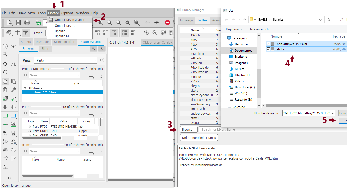
The use of the Fab library is required for Eagle, as well as for the attiny45, they are included in the following file.
Fab library
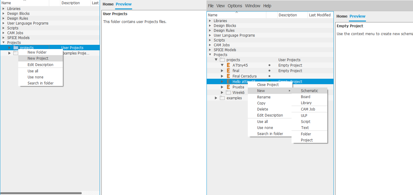
After installing Eagle, it should start, a menu of options appears.
-
To start you have to create a new project and then create a new scheme.
-
It is necessary to add the fab library and those that are required, based on the
component, you can search the internet for the library, in the same way, Eagle has
libraries available to be installed.
-
I'm going to add an avrisp, for this there are two ways to expand the fab library or do
the search.
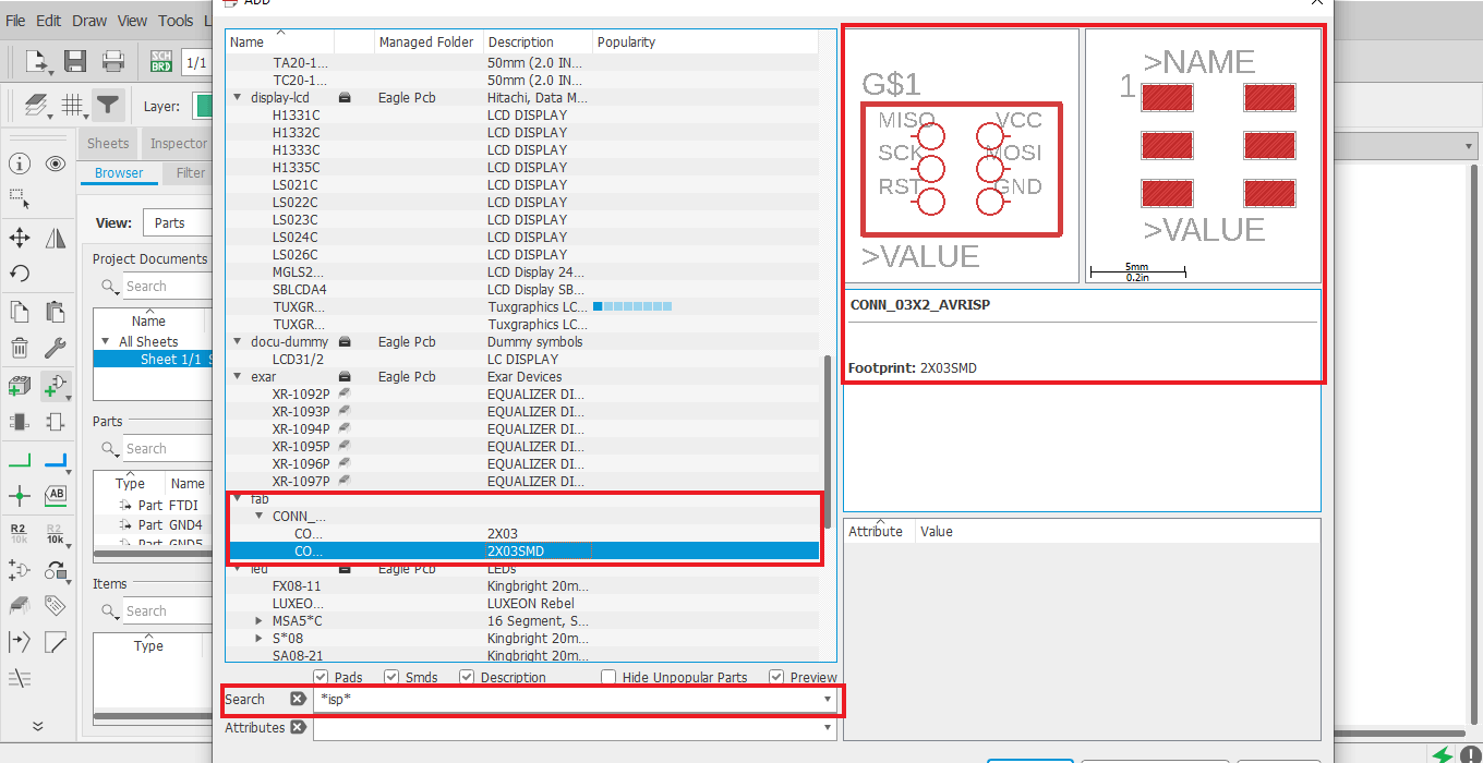
-
After adding each component, the connection between them must be made.
With the net icon, the components can be connected.
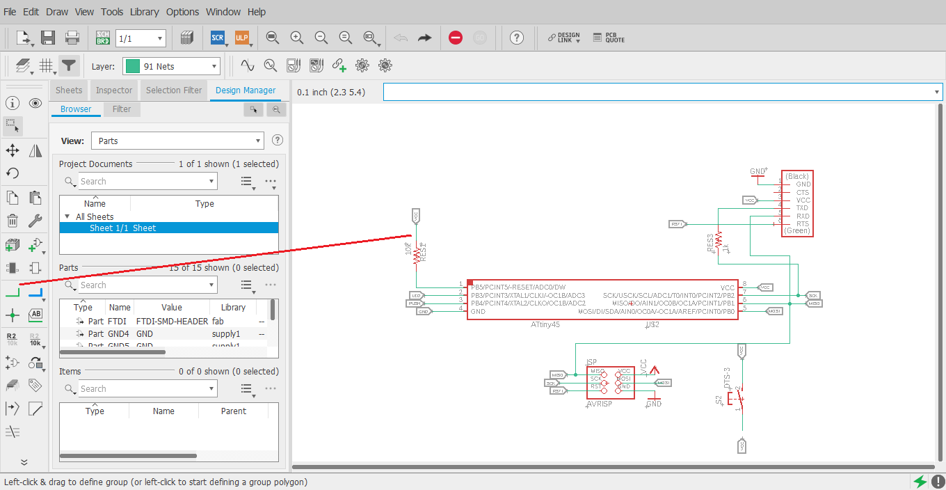
-
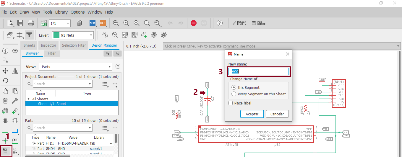
After adding the connections (net) using the name icon, its respective name is assigned
depending on the component, this allows an easy identification of the connection. To
name the connection select the name icon and then click on the connection.
-
In the case of resistor, add it without value (R in fab), that data can be added using
the "value" icon.
-
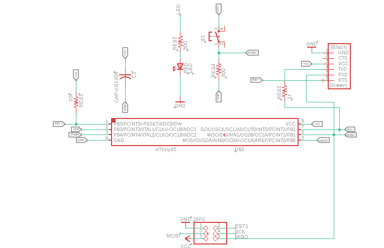
My final scheme.
-
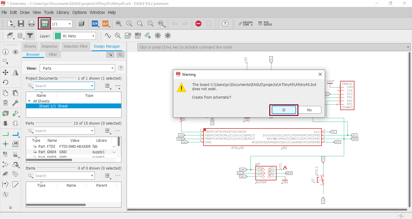
Now you have to create the board layout by clicking on the Generate / switch to board
icon.
-
My final scheme.
-
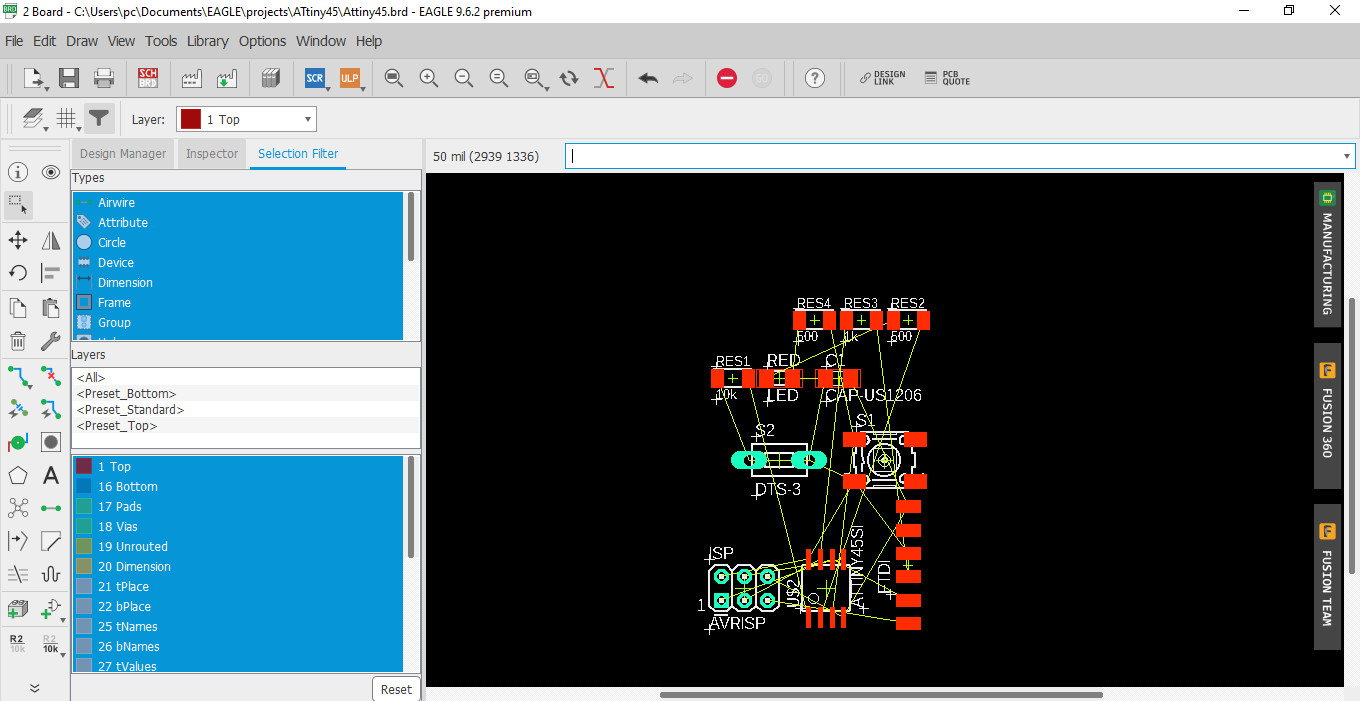
All parts are grouped in the lower left corner. To move them you must select and drag
them with the mouse.
-
To apply a command to a component, you just have to choose the command (icon), then
click in the center of the component, if you see a sign (+) appears in each component.
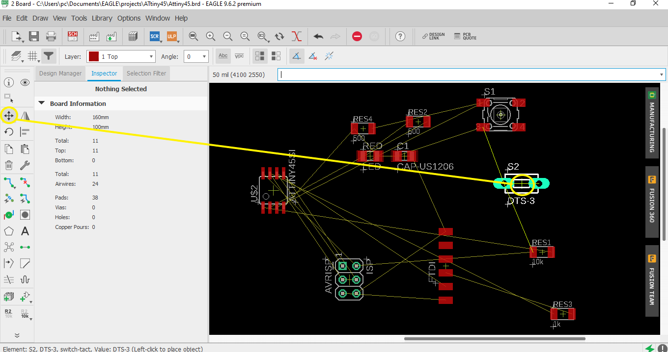
After dedicating time to a good distribution of the components, avoiding that the lines cross, the following result is obtained. -
The yellow lines are a type of wire that represents the parts that are connected. These
junctions can be automatically routed by clicking the Autorouter icon., Of course this
should be done once you have a good layout.
-
In my little experience I suggest that you use routing manually, because it allows you
to decide the path or shape of the trace.
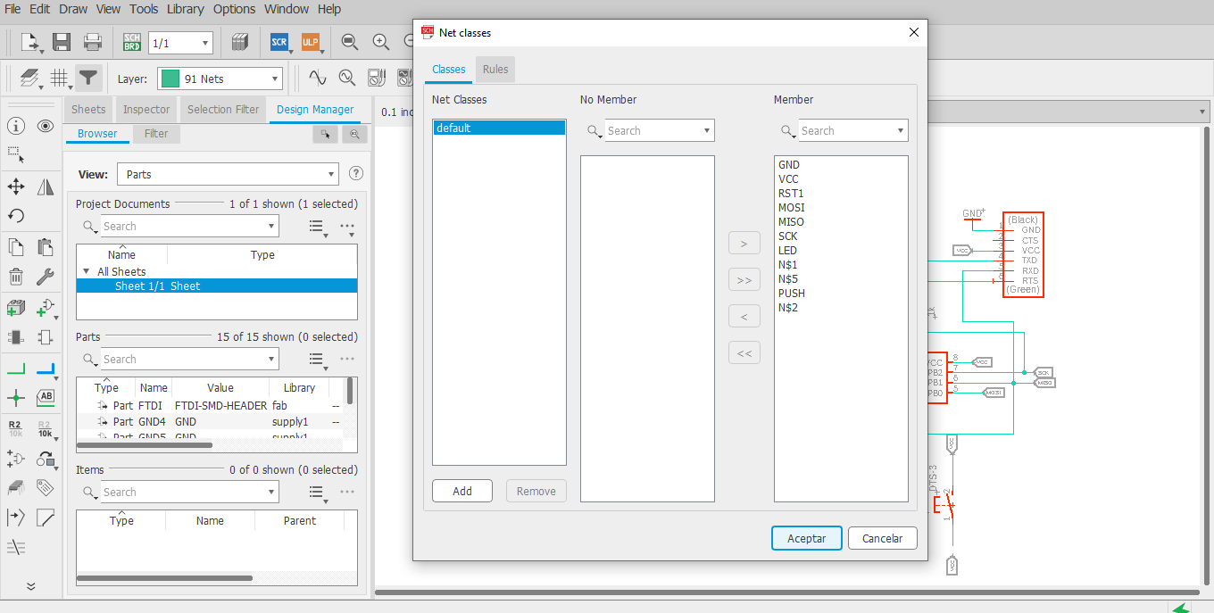
-
Power signals require a larger track width, to ensure Amps will run on these highways
without melting them.
If we want Eagle to know about this circumstance and act accordingly when executing the
Autorouter, we must tell it what the power tracks are and what characteristics they
should have.
In the Edit menu select the Net Classes option. Ae can be done from the schematic as well as from the PCB, in both cases it is the last option on the menu.. The following window will open:
-
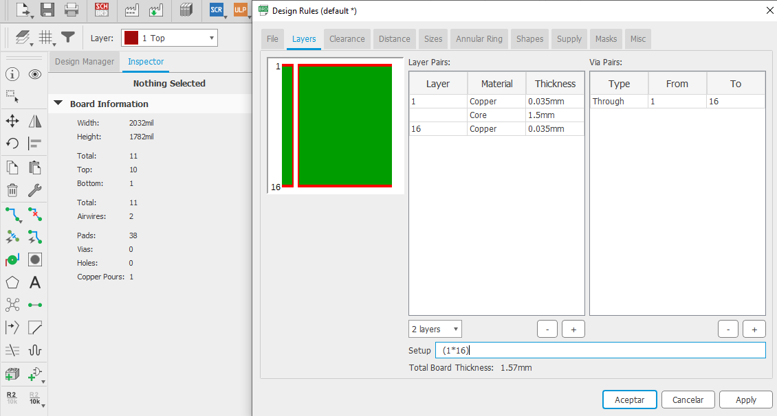
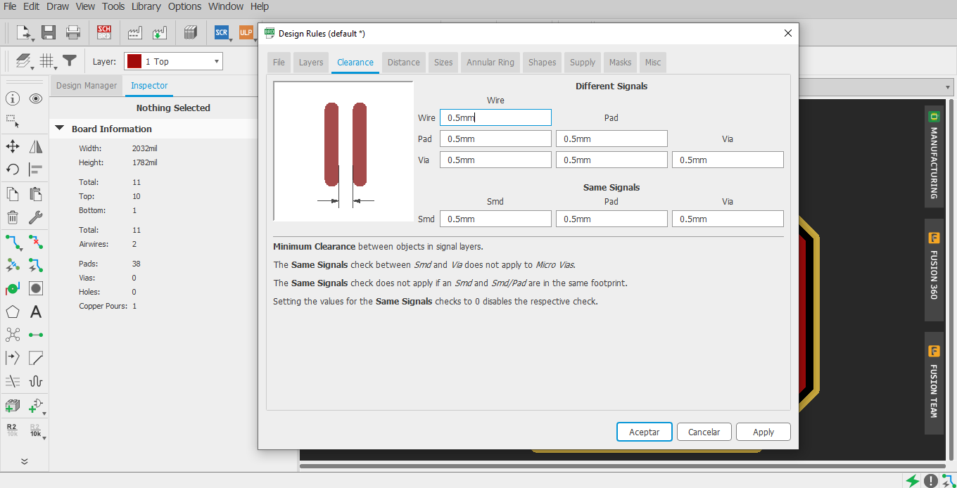
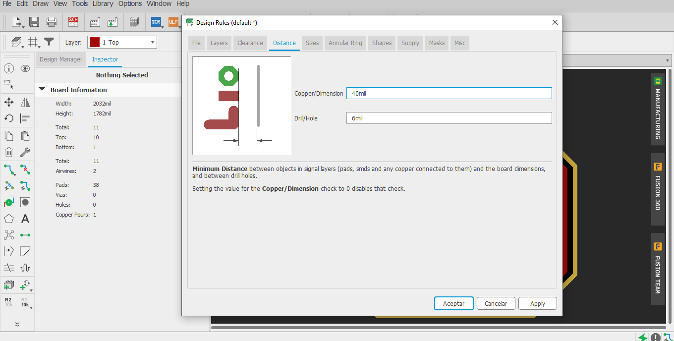
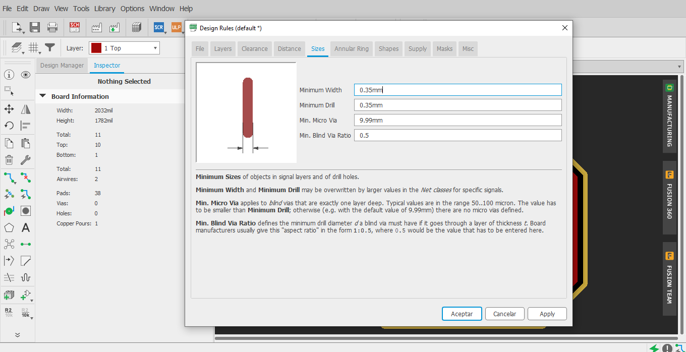
On the other hand, the design rules must be established, this is done once the board is
finished, for this in the edit menu, select "desing rules"
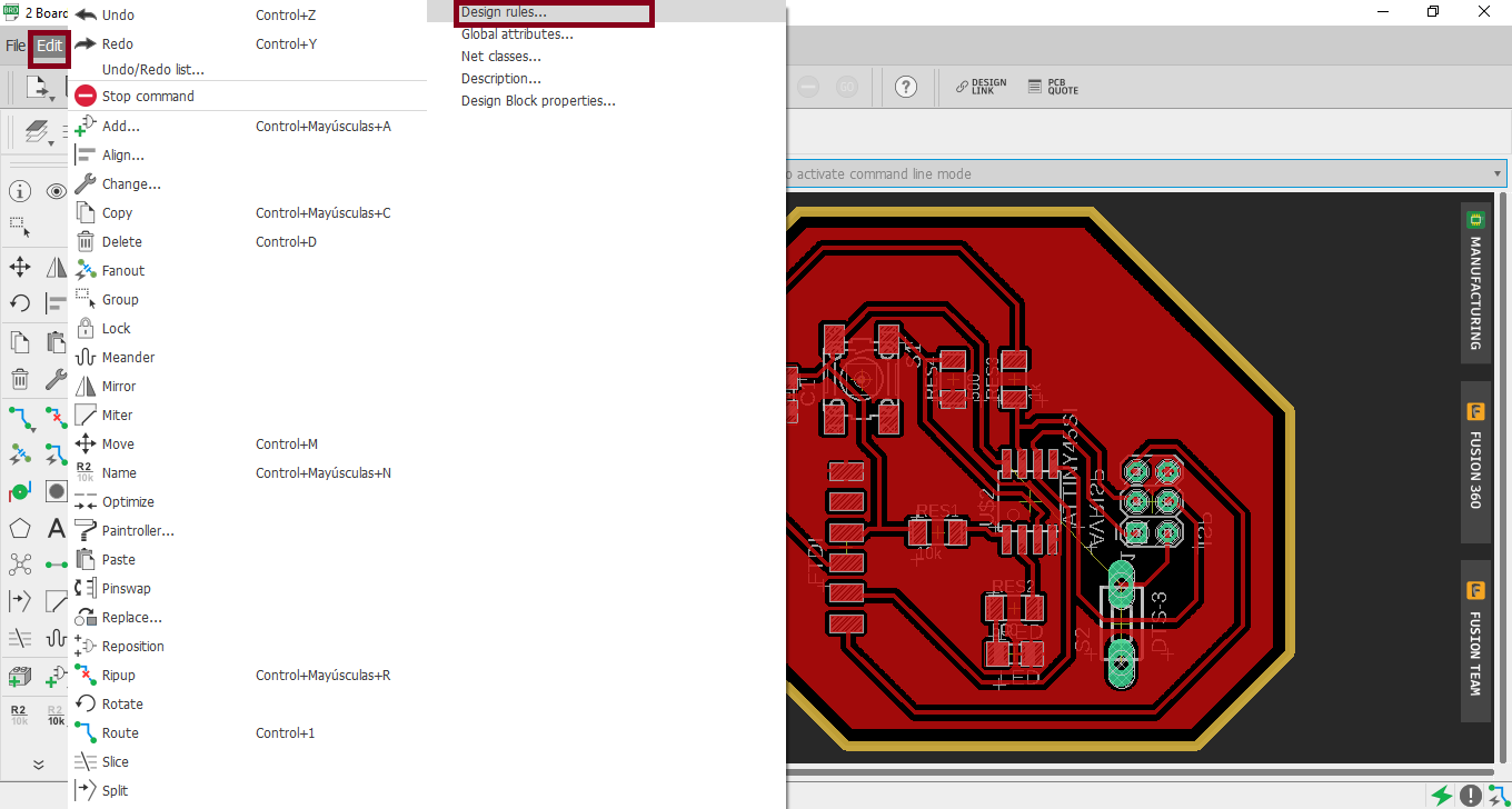
Each of the values will be based on the needs you have. Each property or parts that comprise it are shown below.
Layers
Clearence.
Distance.
Sizes.
-
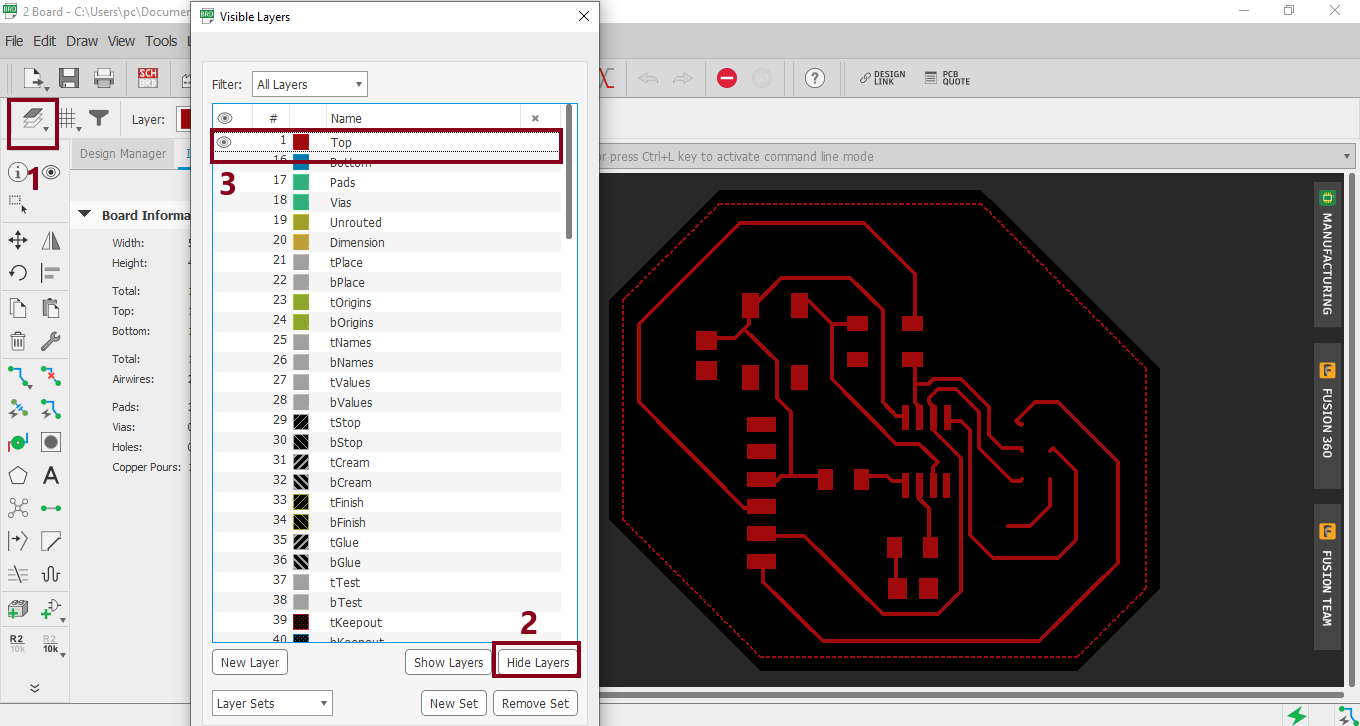
Export png . Two png files must be exported for milling. One for the strokes and one for the outline. First go to the Layers Settings and disable all layers except the Top
-
The next step, it is to export as an image.
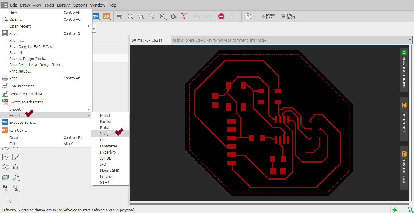
-
The next step, it is to export as an image.
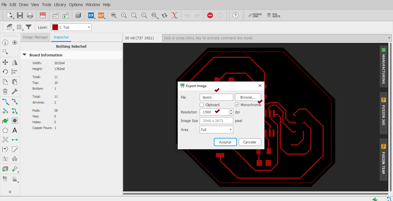
-
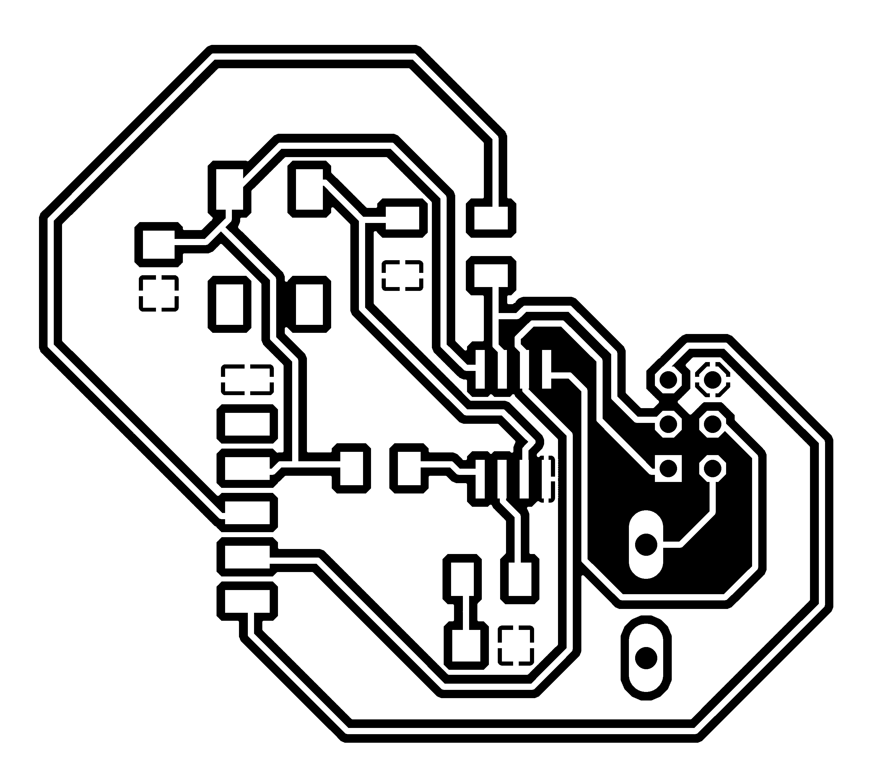
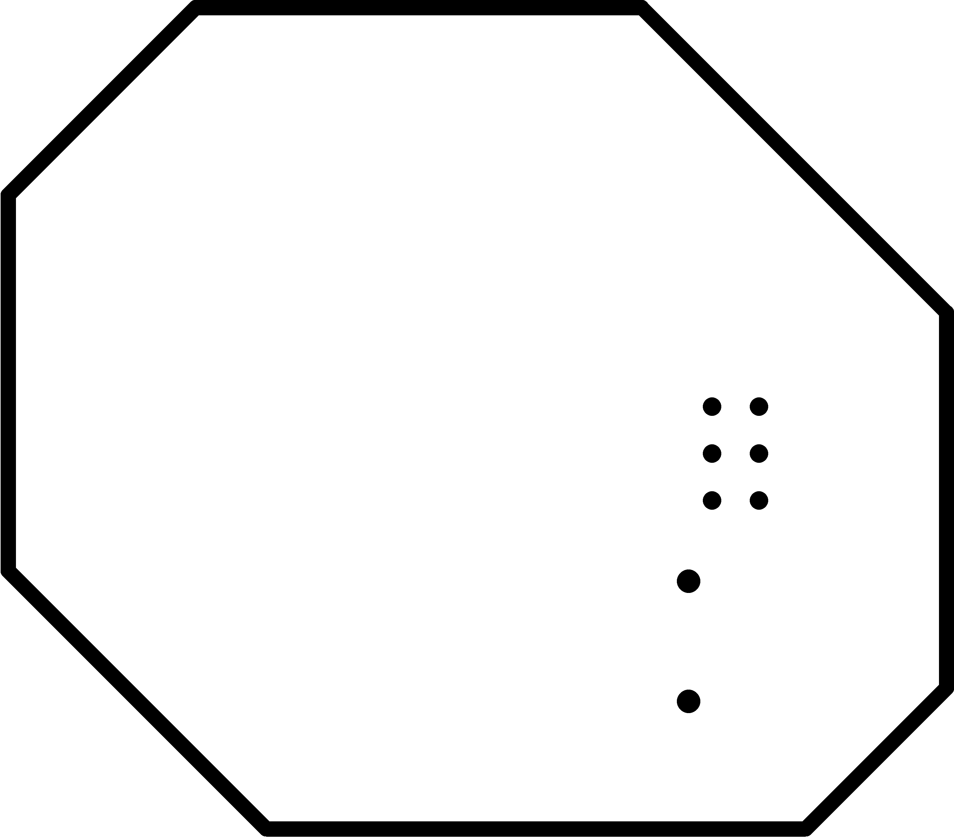
PNG file with traces.
- For contours, again select Layer settings and enable only the dimension layer.
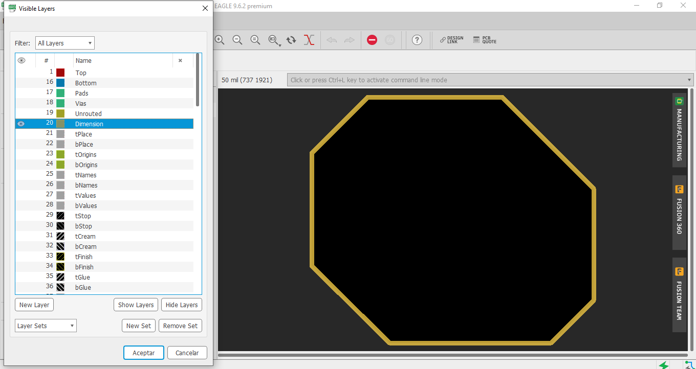
-
PNG file with lines.
-
Using the fabmodules.org tool, now we must consider the marked data, these are a
function of the milling machine to be used, as well as the tool.
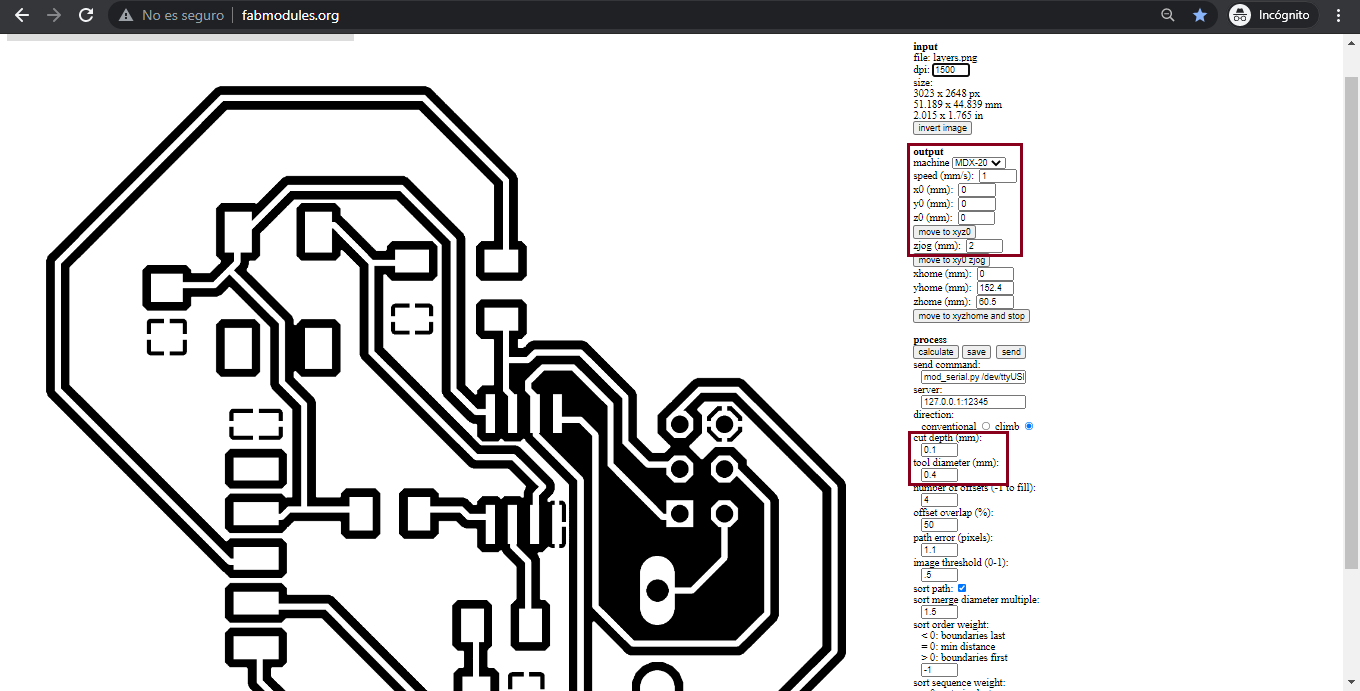
-
The process is repeated to calculate the dimensions.
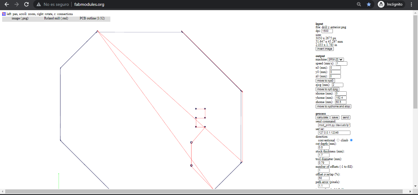
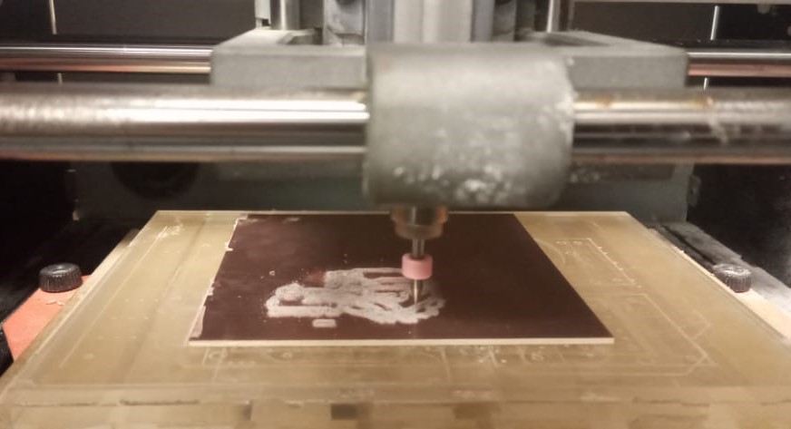
Following the same process from week 6, now in the Roland srm-20 milling machine software
you have to set the initial position for the axes: x, y, z and upload the generated file to
fabmodules.org, the first file to be load is the one that contains the traces.
Finally the board is ready with all its components.
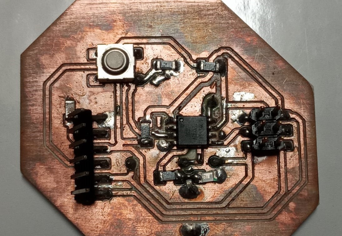
After programming and documenting it, in the "Embedded programming" assignment, it can be seen that when the button is pressed, the led turns on.