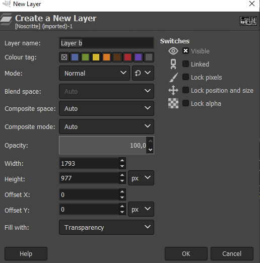
Week 6
Goals of the week
Group project:
use the test equipment in your lab to observe the operation
of a microcontroller circuit board.
Individual project:
redraw an echo hello-world board,
add (at least) a button and LED (with current-limiting resistor)
check the design rules, make it, and test it
extra credit: simulate its operation.
This is the link of the group assignment
Hello board
In order to complete the individual assignment, I chose to redraw the hello board starting from the Attiny 45 board that Professor Neil uploaded on the schedule.
Bom:
-1 avrISP;
-1 Attiny45;
-3 Resistors (one of 10 k ohm, one of 1 k ohm and one of 150 ohm);
-1 capacitor;
-1 orange led;
-1 pin header 1x6 (vertical)
-button
ISP
"The FabISP is an in-system programmer for AVR microcontrollers, designed for production within a FabLab. That is, it allows you to program the microcontrollers on other boards you make, using nothing but a USB cable and 6-pin IDC to 6-pin IDC cable. It's based on the USBtiny and V-USB firmwares, which allow the ATtiny44 to perform USB communication in software. Programming can be done through avrdude."
I used it during week 9, week 11
and in my Final Project
Add a library
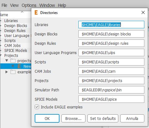
This is a very useful link to learn how to add a library. So, I first dowloaded the fab library from my GitLab Account, I unzipped the library folder (fab.Ibr), then I opened Eagle. There i clicked on Option and Directories, finally I changed the path writing my data (or better, the path to the folder on my computer).
Once the fab library was visible and integrated with other libraries available on Eagle, I started to build my schematic.
Schematic Vs Routing
In the schematic we just have to insert from the libraries the components of our board creating the links already and possibly naming the various components and assigning them values (so everything will be clearer in the routing);
in the routing, instead we have to insert the components exactly where we will solder them and then we have to create the right traces to connect them.
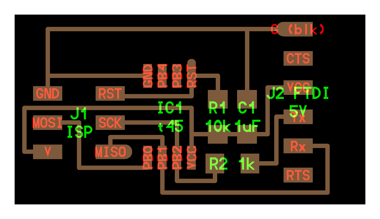
Schematic
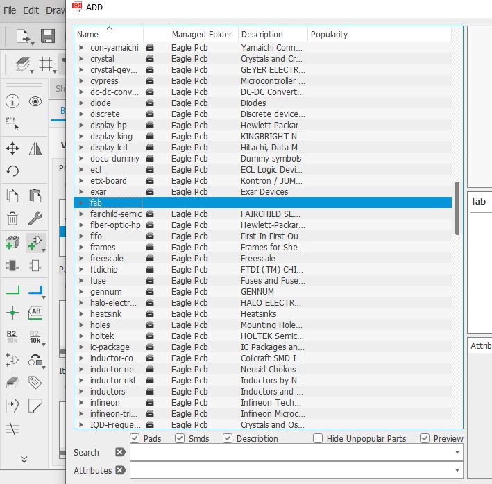
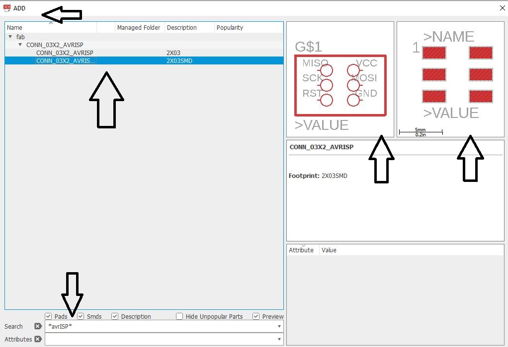
In order to select the components in the schematic, you have to click on the "add" button and select the component from the library. You can quickly search writing the name in the form between two * (for example *avrISP* ) to be sure that, even if the name is a little bit different, the program will be able to find it. You could not see the name of the componenets (it happened to me): in this case just make sure the curtain is fully open! Once I finded the right component I just clicked "ok" and than "esc" before selecting the others repeating the same procedure.
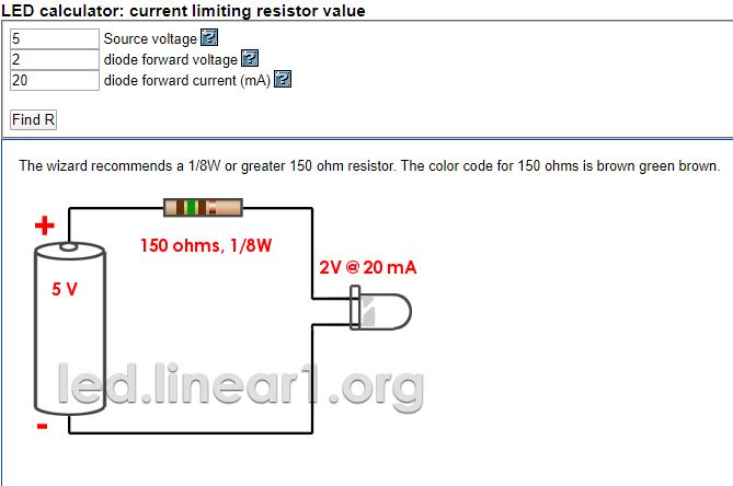
I had to put at least a led and a button. I chose the orange led and calculated the resistor value using this really helpful link an it tourned out that the resistor should be a 150 ohm one.
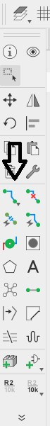
Below you could find the toolbar with an arrow that indicates the tools that you absolutely have to use.
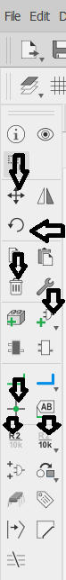
In order:
MOVE (to move the components)
ROTATE (to rotate the components)
DELETE (to delate the components)
ADD PART (to add the components)
NET (to create the logical nets)
NAME (to give a name)
VALUE (to give a value)
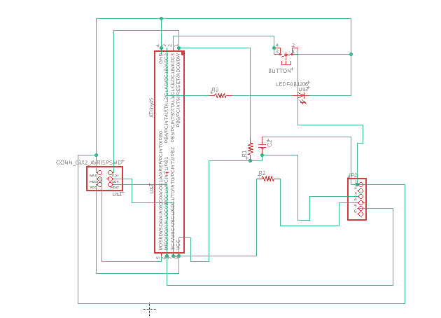
This is my schematic:
Board
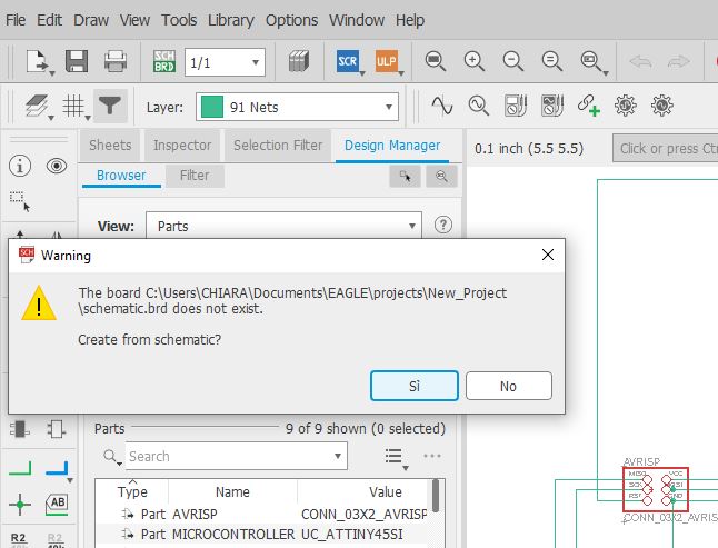
Once my schematic was ready I clickedd on "File" and then on "switch to board" button.
This is the warning, obviously I selected "yes" (sì)
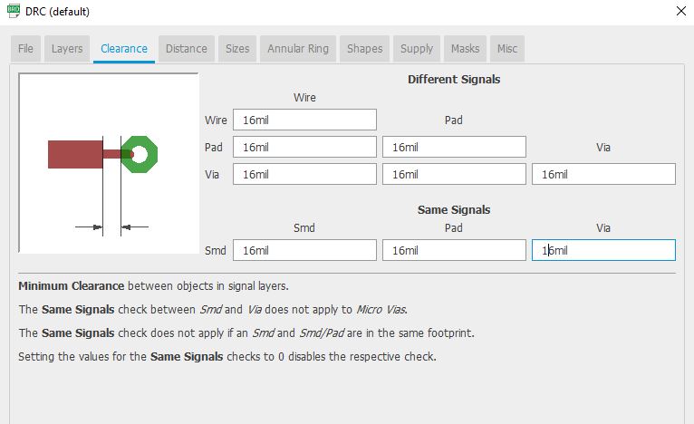
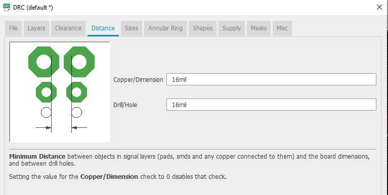
and 16 mil in the distance.
Thanks to the test we made during the fouth week, we know that 16 mil is the minimum distance that could be between our traces.
So, at the beginning my components where out of the board but still with the net links. I just moved them with the "move" tool and created the traces with the Route Airwire tool
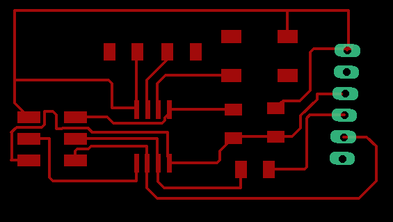
This is my board:
I exported it in monochrome and 1000 dpi
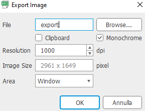
Some important tips before Exporting
The first time I exported my board in png, I forgot to cancel all the writings (name, values...).
Then, following my tutor's advice, I:
- clicked on "view" and "layer setting",
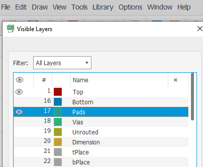
- hidded every layers except "top" and "pads", - clicked "ok".
Then it could seem that every writing was delated but it was not, there were still some of them (for example into the circles)
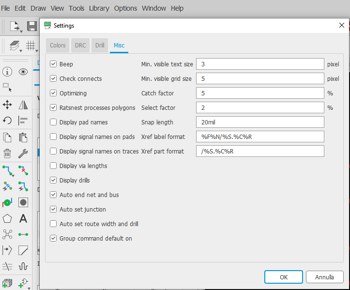
- So, I clicked on "Option" (in the menu),
- then on "Set", and on "misc" and I deselected all these voices:
display pad names
display signal names on pad
display signal nemes on traces
display via lenghts
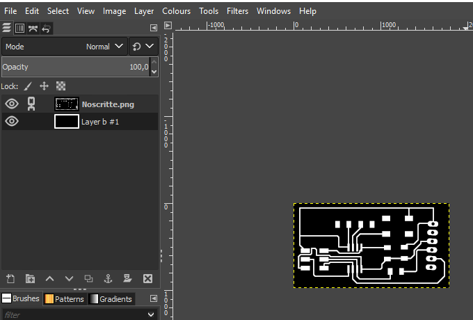
Gimp
(This was the the most difficult and frustrating part for me. It's not difficult the process itself, when making sure all the settings are right, otherwise you can't even do the simplest steps.)
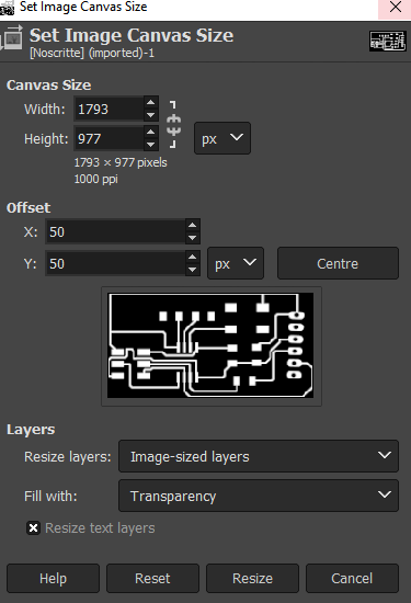
Anyway, first of all I imported the .png file on Gimp and clicked on "Image", "autocrop image" to delete all the unnecessary, then I clicked on "Image", "canvas size" and I added 100px to both height and width and centered the image. (In order to obtain the frame that I used for the outlines and to give more space for the traces).
Traces
To obtain the traces file I created a new Transparent level. The opacity must be absolutely at 100!
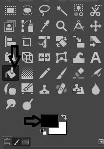
I placed the transparent layer underneath the layer of my board. Then, I selected the Bucket fill tool and the black color, so I clicked into the imagine but making sure to have selected the new level.
Finally I exported the traces file.
Holes
For the holes I created another transparent layer. This time I've placed it above the level with the tracks. I filled the transparent layer with the bucket tool, this time using the white color. I selected the holes with the fuzzy tool selecting the image layer and hiding the white layer. Then I exported the file

Outlines
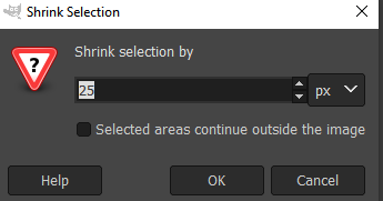
In order to create the outlines file I created another transparent layer that, again, I put above. I filled it with the black color and then I clicked on "Select" and then "All" in order to select all the level. Then I clicked on "Select" and Shrink and I wrote "25" in order to subtract 25 pixel. So I got a smaller rectangle that I filled with white with the Bucket Fill tool.
Finally I exported also this last file!

Mods
Following the same process of Week 4 I imported the file in Mods in order to obtain the .rtl file to upload in the mill.
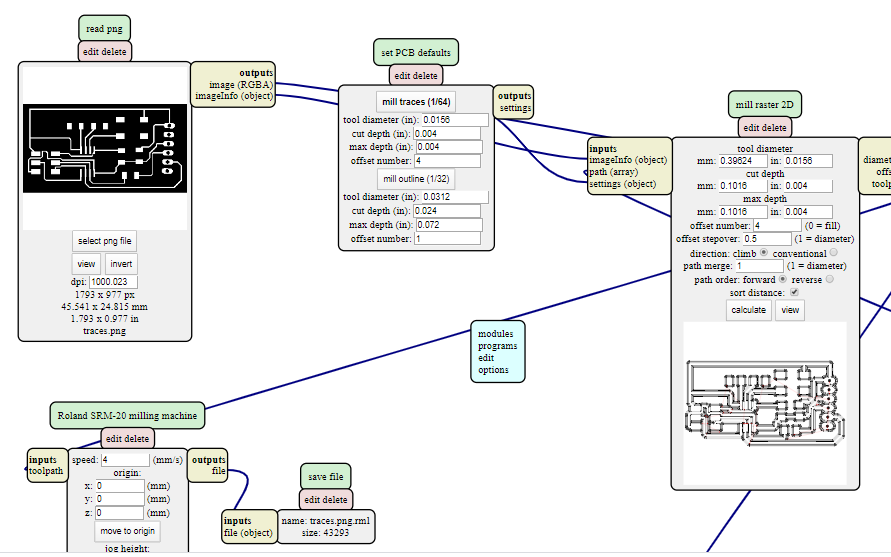
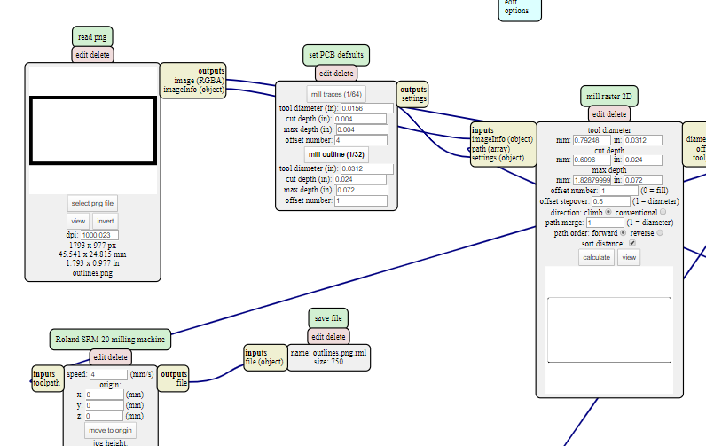
I don't know why, but I had some problems to convert the holes file, so I used this older Mods and I managed to do it (even if it is a little bit different)
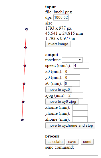
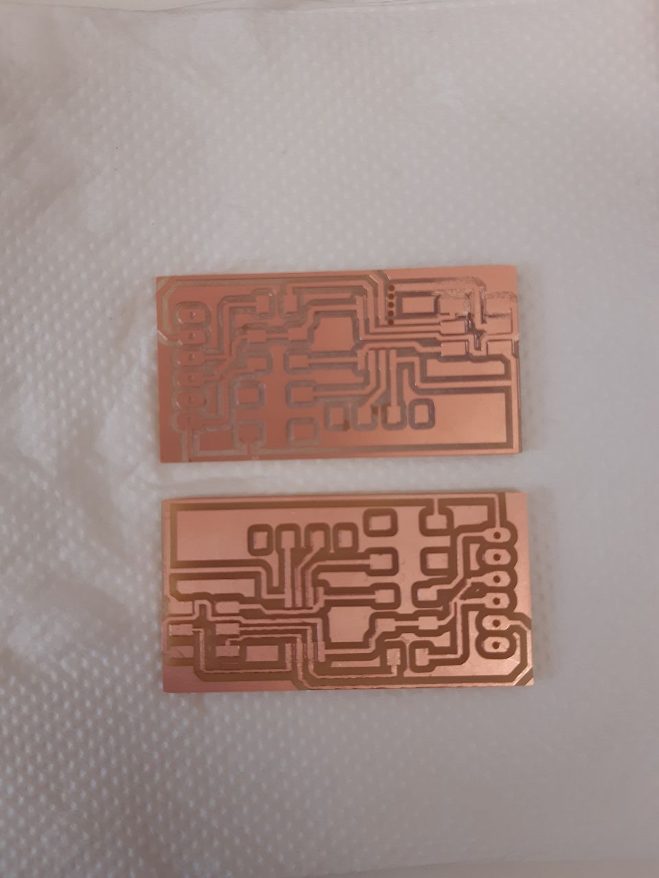
Milling
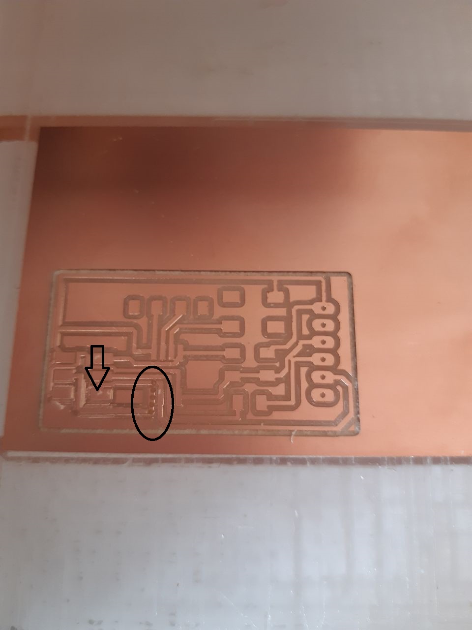
I had to mill the pcb twice because I had a problem: something went wrong with the hole file. It milled them much smaller and in the middle instead of on the right. It also did not milled the left side very well, probably because there was a difference in height in the sacrificial plane or because the tip was ruined.
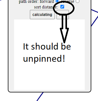
I checked the dimensions and they were identical. My tutor told me that this could be because I imported the png file in a different mod (the old one) than the one where I imported the traces and outlines file. So I understood what was the problem that prevented me from getting the .rml file from the new Mod (which is why I used the old one). Simply the sort distance option had to be unpinned
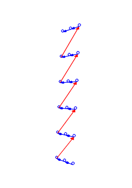
So I exported the .rtl files of both traces, outlines and holes, all from the same mod. I changed the tip and took, just in case, the Z a bit more to the left.
This is the result:
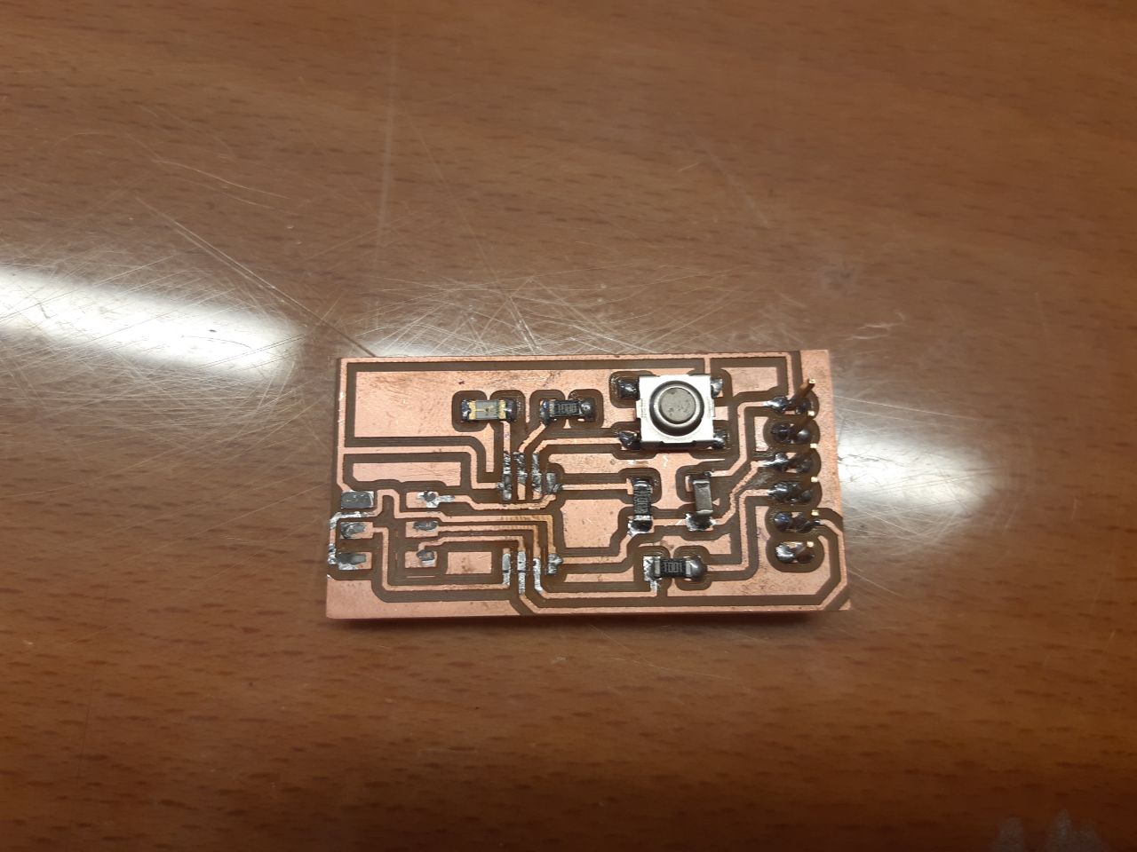
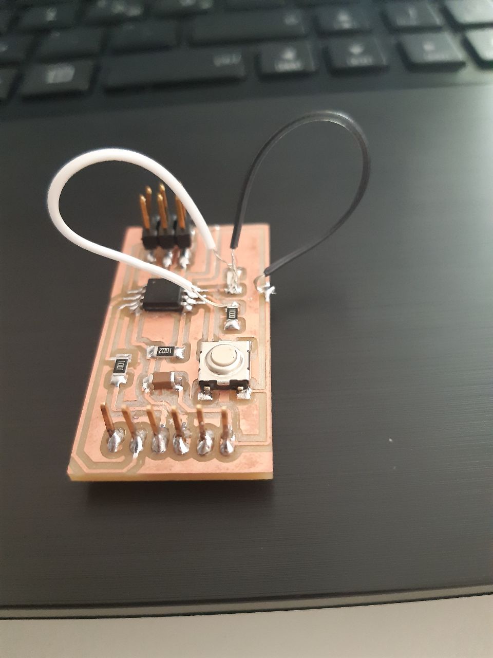
Programming
During the programming phase I noticed some errors: first of all, not having checked the mods files, I didn't realize that milling the card would have created unwanted bridges (not visible in the .png file) both in the attiny and in the isp. Moreover, I forgot to create the trace between the resistance and the led and between the led and ground! Not having the time to modify the eagle file, mill and solder the board again, my tutor suggested me to cut the bridges with the cutter and to create the connection between the led and the resistance and between the led and ground with wires.
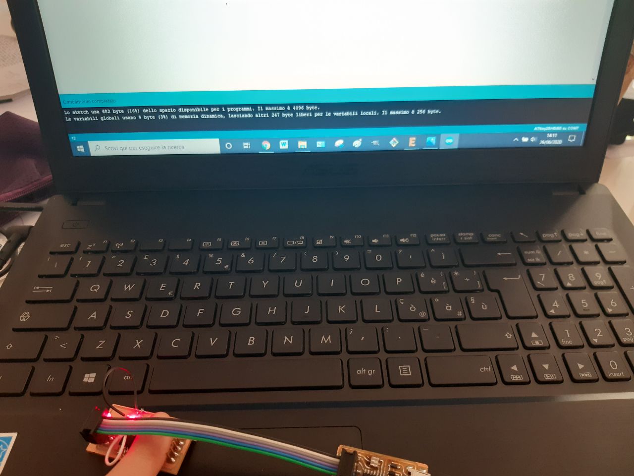
This is the code
Useful links:
add a library
schematic
tutorial
You can find the downloadable files here
Eagle schematicEagle board
Outlines
Traces
Holes