Week 4
The aim of the individual assignment is to make an in-circuit programmer by milling and stuffing the PCB, test it, then optionally try other PCB fabrication process.
February 20th
Part 1
I went to the Fab Academy schedule and through the "in-circuit programmer" link in the "Assignment" section, I arrived in the page called "Embedded Programming" from which I could access the documentation of a guy called Ali. From his page I could download png images of his traces and outlines.

Then I went to this page , I pressed the right key on the icon, clicked on "Program", then on "Open server program" and on "PCB png" (because my files are in png) under "SRM-20" because the cutter of this lab is a Roland SRM-20. The screen that appears is this one:
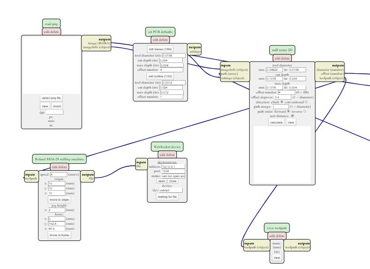
I clicked on "select png file" and chose the image of the tracks I had downloaded, so in the square on the right I pressed on "mill traces 1/64" with reference values that must not be changed.
The resolution of the image must always be dpi=1000 .
To make the milling start from the origin, give the x, y and z value 0.
I preferred not to send directly to "print", so I deleted this block.
Then I clicked on the icon at the top left, pressed the right mouse button and selected "modules", "open server modules" and "file save". I placed the new block in the same position as the one I deleted.
I then clicked on "file object" under "inputes" and on "file" under "outputs". This way the system connected the two blocks with an arrow.
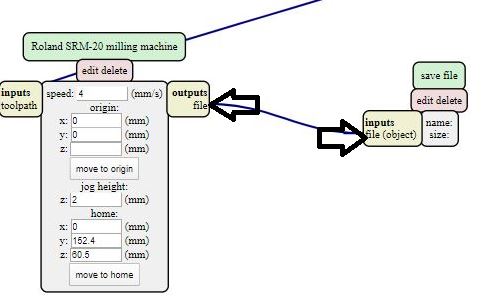
After "calculate" the system converted my image to the file that I will insert in the cutter.
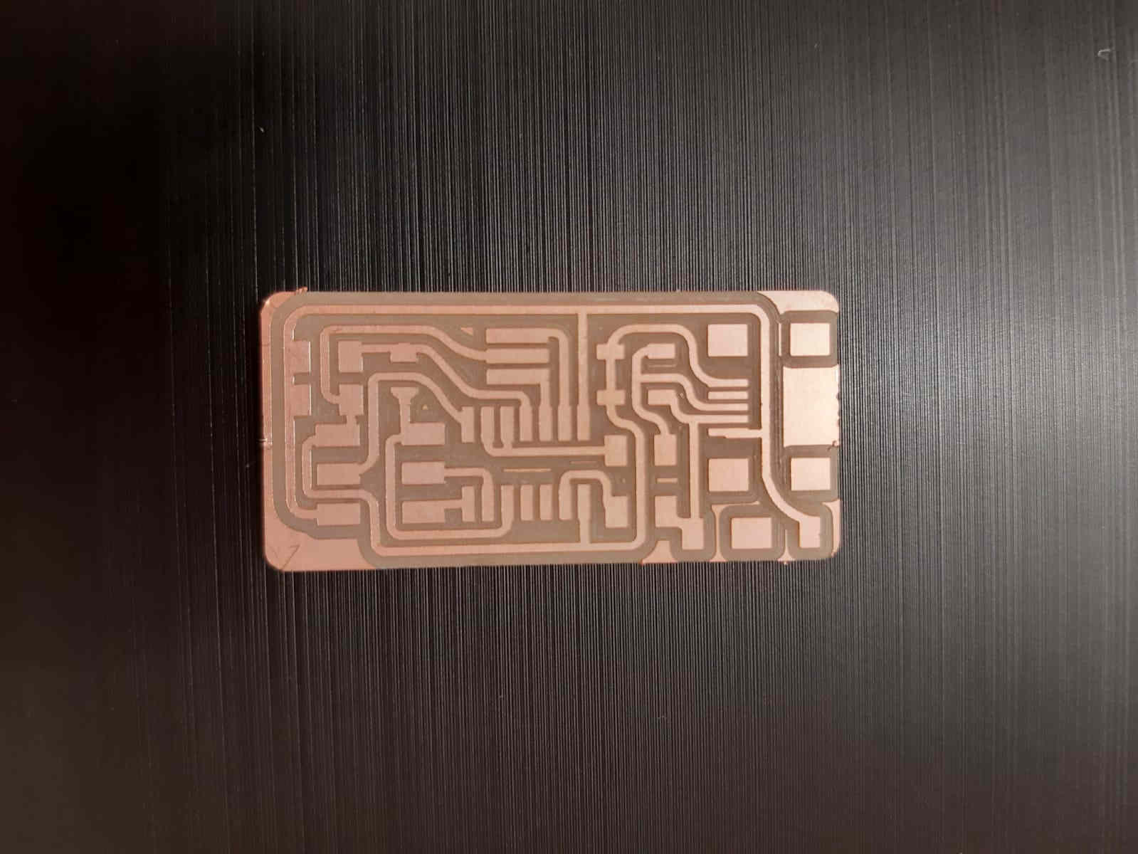
With the same procedure I make the file for the outline.
Part 2
At this point I was ready to mill
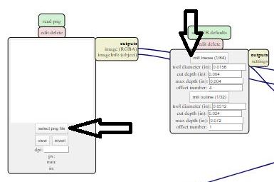
The software I used is called VPanel and is connected to the milling machine in our laboratory, a Roland SRM-20. From Simone Guercio's website
I took the link to the User's Manual.
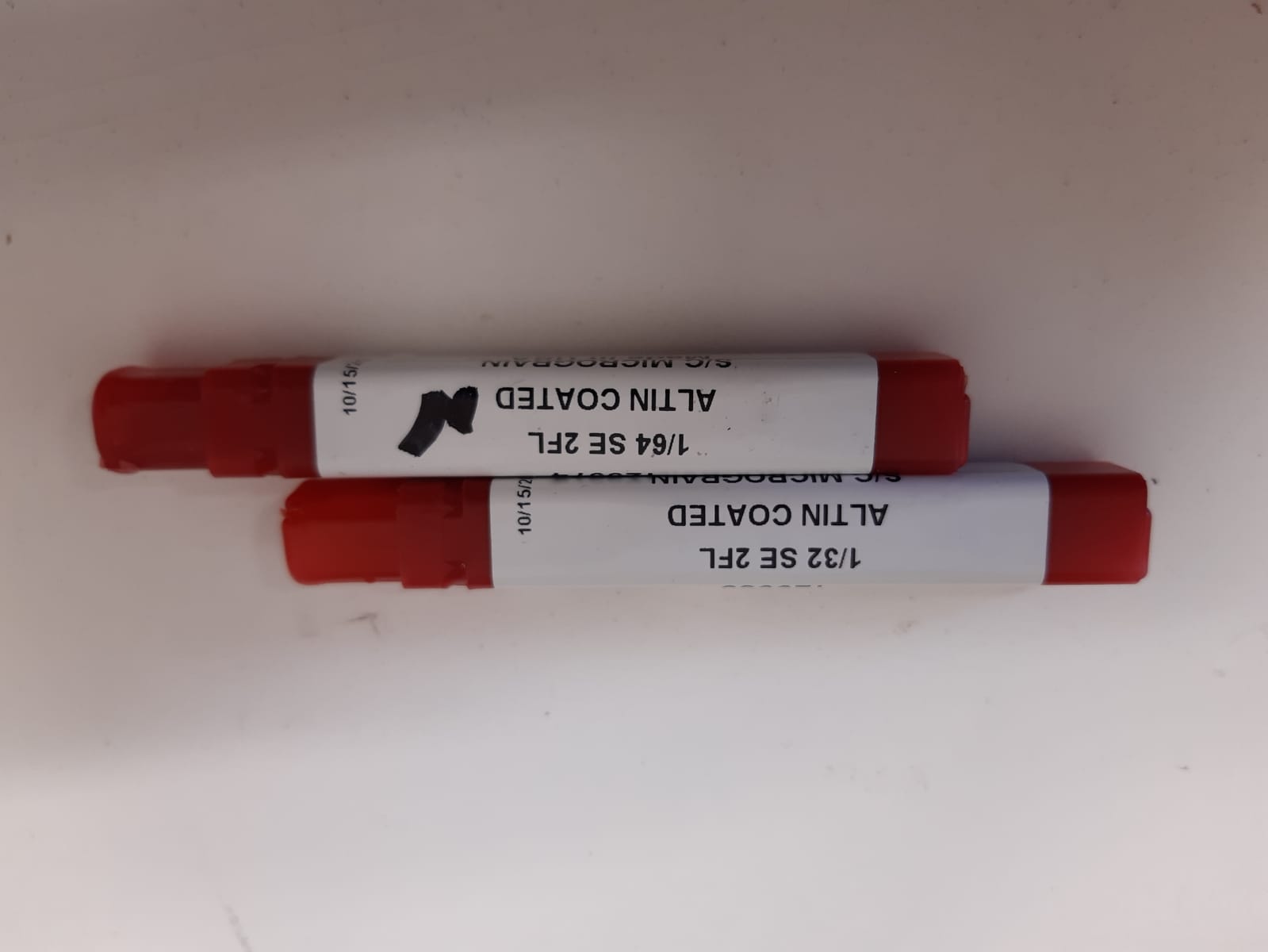
In order to mill the PCB it is first of all necessary to fix it in the working surface with double-sided adhesive tape (it is absolutely necessary that it does not move). Then I inserted the end mill 1/64 (the one to mill the tracks) into the spindle. Initially it didn't mill well because I didn't exert enough pressure when I inserted the end mill (this is a small but decisive trick).
it is therefore necessary to fix the origin (X/Y).
As you can see from the image (taken from the above mentioned manual) I pressed the arrows (box 5) to position the spindle and end mill where I wanted it to start milling (bottom left of the PCB so as not to waste material).
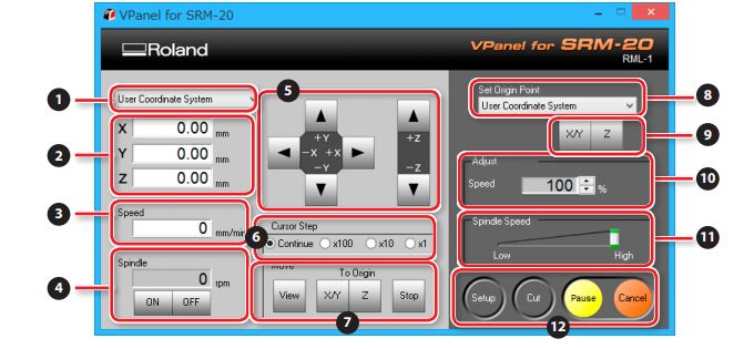
To set Z, however, I loosened the spindle grip slightly, touched the endmill in my PCB, tightened the spindle again, set Z and raised the spindle slightly.
At this point I inserted the RML file by pressing on cut (second button at the bottom right). Taking into consideration the screen made by the manual, note that at point 2 there is the option "delete all".
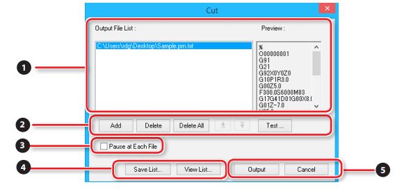
I initially deleted the last file inserted in the program and from the "Add" button I selected my file and pressed "Output" (section 5).
At this point the milling machine started to weld.
I did the same process for the outline but with endmill 1/32.
February 23rd
At this point my pcb was ready to be welded.
I then compiled a "Bom" (Bill of materials) writing the name of every compenents I was going to use and paste them next to their name. The order was not random, I chose it according to the method I thought was best so as not to have any impediments during welding.
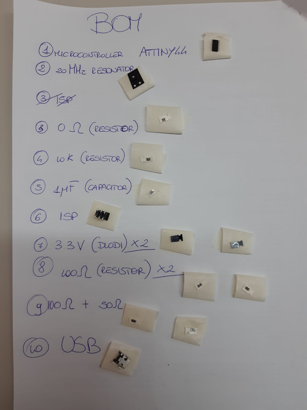
Note that there is a very serious error (but I noticed it late when the card was not working).
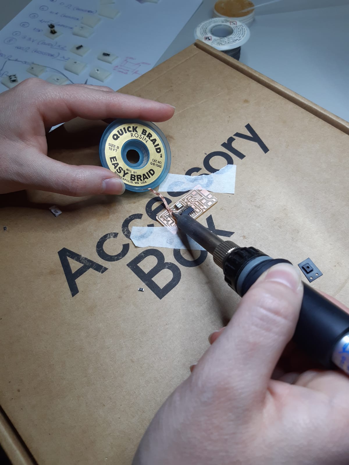
Once I had all the components ready and in order in the soldering station, I was able to turn on the soldering iron at a temperature of 330 degrees Celsius and also the vacuum cleaner so that it sucked all the fumes.
My tutor advised me to apply some flax before inserting the components and initially I did so, then I realized that I preferred soldering without.
Honestly it wasn't easy because the components sometimes moved around, I didn't have a steady hand, and I always tended to melt more solder than expected.
The solder has to tie the component to the track, but you have to be very careful that there are no unwanted connections and that the desired ones work.
The ideal situation is to put the right amount of solder, but between putting too little and putting too much is preferable the second option. Putting too little in fact can result in a missed connection (and is solved by adding a bit 'of solder), if you put too much, however, may not create any problem, and if not, the situation is resolved by applying a copper braid over the excess solder and place the iron on top so as to melt it and stick to the braid (a procedure that I have done perhaps too often).
As said before, there was a big mistake in my bomb: I inserted a 100 and a 50 ohm resistor instead of a 1kohm and a 0.5 kohm one!
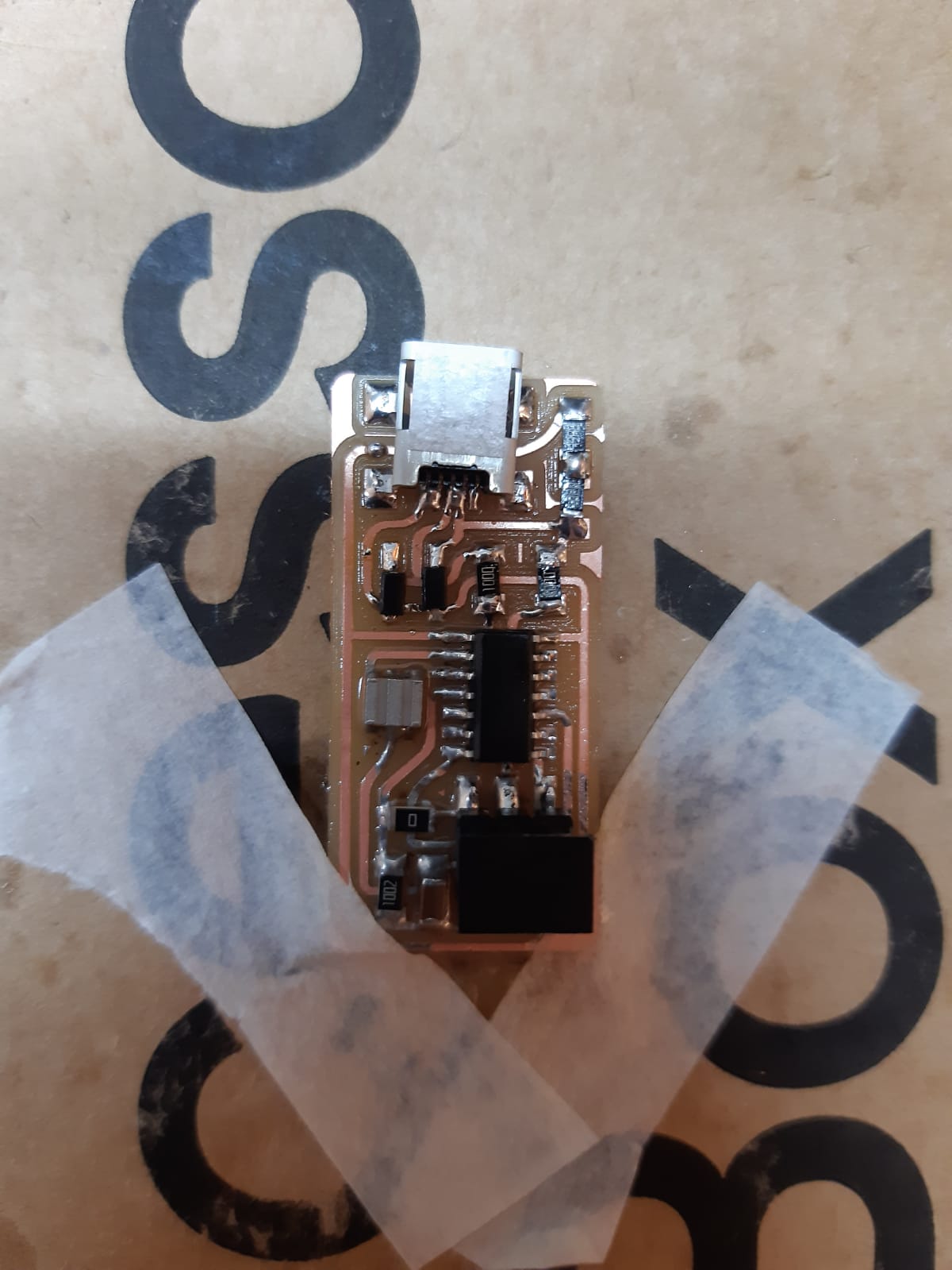
This is my card welded in all its faults before desoldering
February 24th
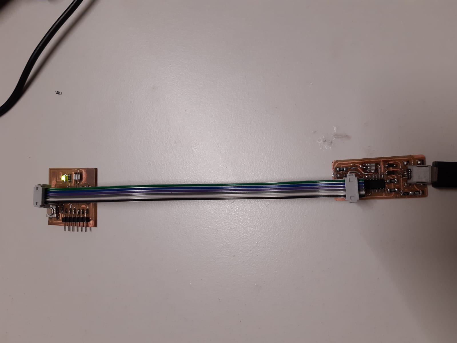
The card I soldered will be (if it works) the one I will use to program all the other cards I will make. Our tutor has explained that we will always have two cards: one that acts as a bridge between the card we want to program and our computer and the card we want to program. The first one is called "programmer" (and it should be this one), the second one is called "programmee".
But first we have to make sure that our programmer works. There may be hardware problems (the board is soldered wrong, there are one or more components that are not wrong, or the schematic is wrong).
Using the tutorial
"FabIsp Production and Programming, Guide for cutting, assembling and programming your first FabISP" , I made the first test: the smoke test (if the pc tells me that it requires a too high supply it means that our board is short circuited and therefore done wrong). Fortunately my board passed it.
I then downloaded and installed Atmel studio from the link . Avr will allow me to use the Atmel toolchain.
In point 2 of the paragraph "Windows Software/Drivers Install" , I found the link to download my driver on Adafruit. The drivers allow you to communicate with the programmer.
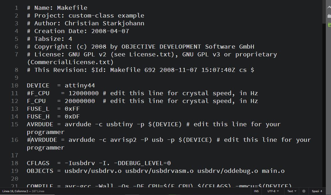
I then downloaded the firmeware from the link Download the FabISP Firmware in step 5. Once zipped the folder, I opened the "Makefile" document with my editor (Brackets) and, as written in the guide, I Removed the "#" in front of the line with "usbtiny" in it, Added a "#" to beginning the line with the "avrisp2" in it to comment it out and saved the Makefile.
The firmware is a program that will have to go on our cards.
I then downloaded Make from the link
At this point I could program (or try to program) my pcb.
I have to tell the truth: I had to make several modifications due to welding errors and wrong components. Don't get discouraged if you waste a day or two trying to figure out what's wrong! In my case, in addition to the resounding error of the 100 and 50 ohm resistor instead of the 100 and 0.5 k ohm ones, I also inserted a wrong resistor because someone had put it in the box where I should have found the right one! This is a borderline case, but never trust it! It's very important to always read the numbers above as well. Anyway my pcb wasn't working also because of not perfect welds and ruined by the use of hot air: a means to use with caution.
For convenience I won't publish the photos of all the wrong attempts (there were at least 3).
The procedure is as described in /a Program the FabISP : "Navigate to the directory where you saved the FabISP firmware. If you followed the instructions above, this will be the desktop." In this regard I would like to highlight 2 very important points that could be discounted theoretically but which I have not taken into account in practice:
- It is fundamental that during this phase the computer is connected via a USB cable to a programmer that is connected to our (still) programee;
- if to make order, as I did without thinking about it, you decide to move your make file, remember it because in this case it is necessary to modify the Path in this way:
1. Open the control panel and select "System";
2. select "advanced system settings", environment variables" and then "path";
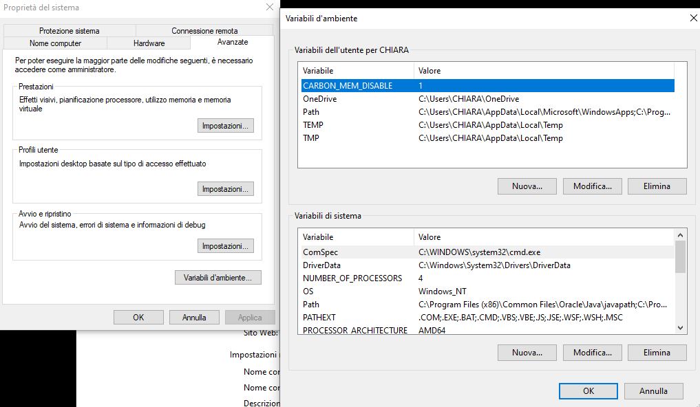
4. select the path you want to modify and press browse to choose the exact point where it is present in our pc (path);
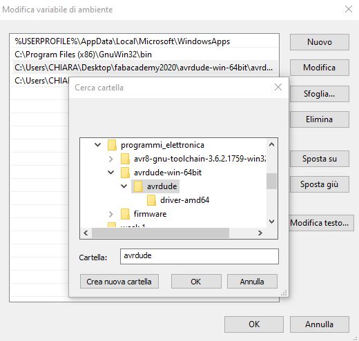
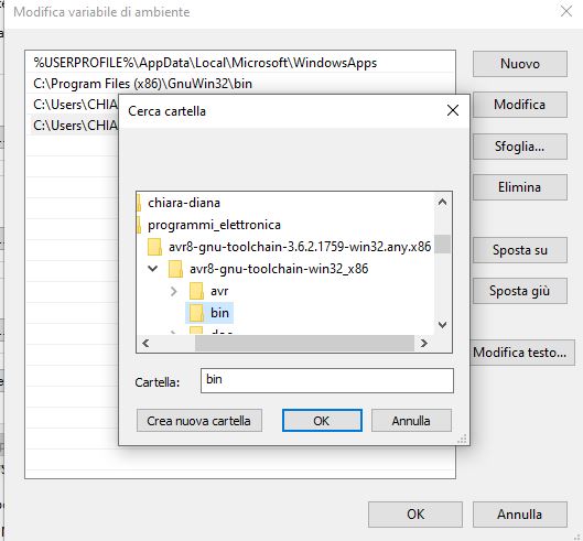
5. finally press "ok" to all tabs.
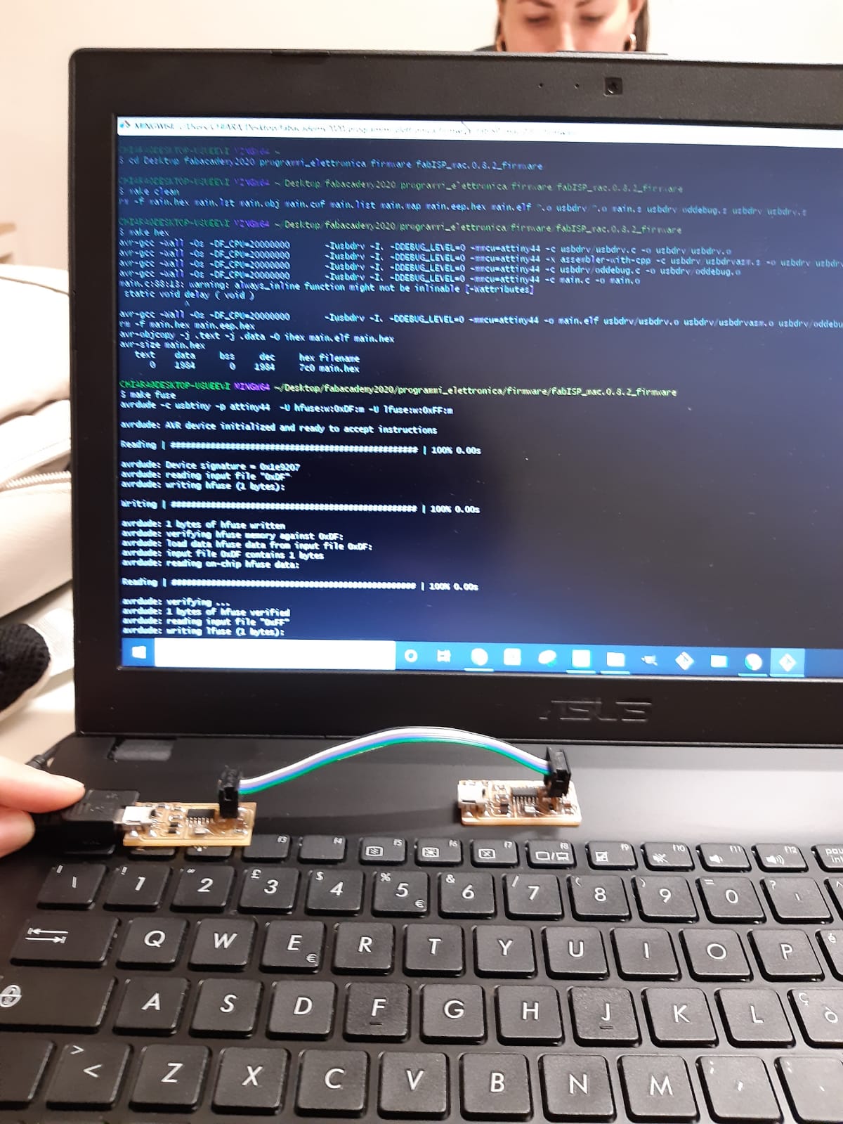
At this point you can finally proceed with the "make clean", "make hex", "make fuse" and "make program" commands on GitBash.
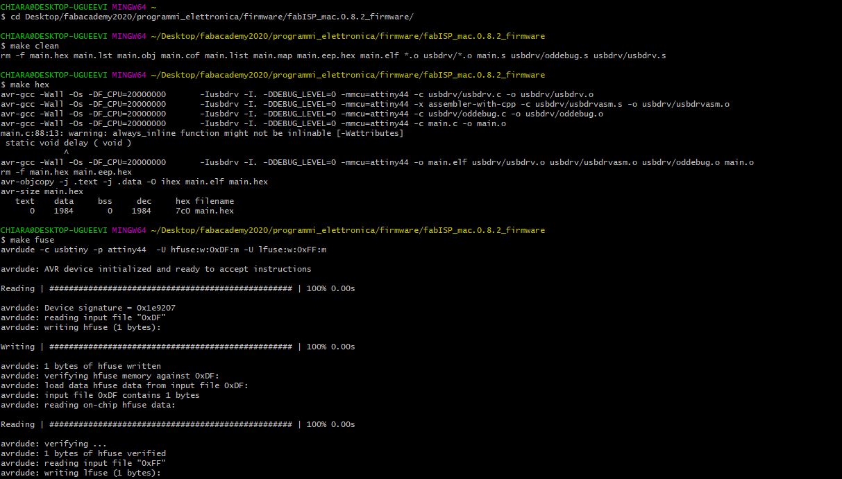
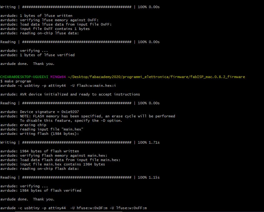
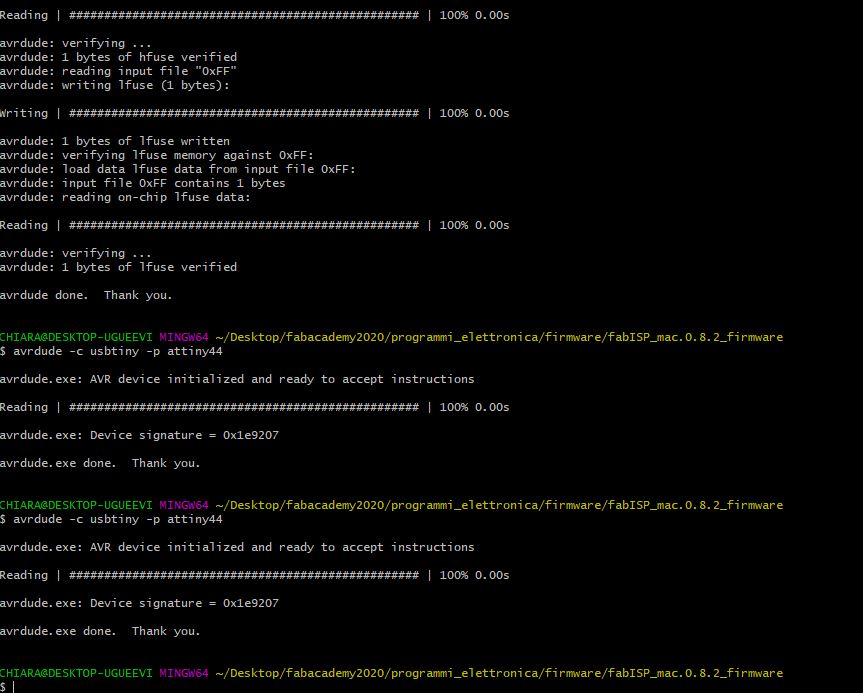
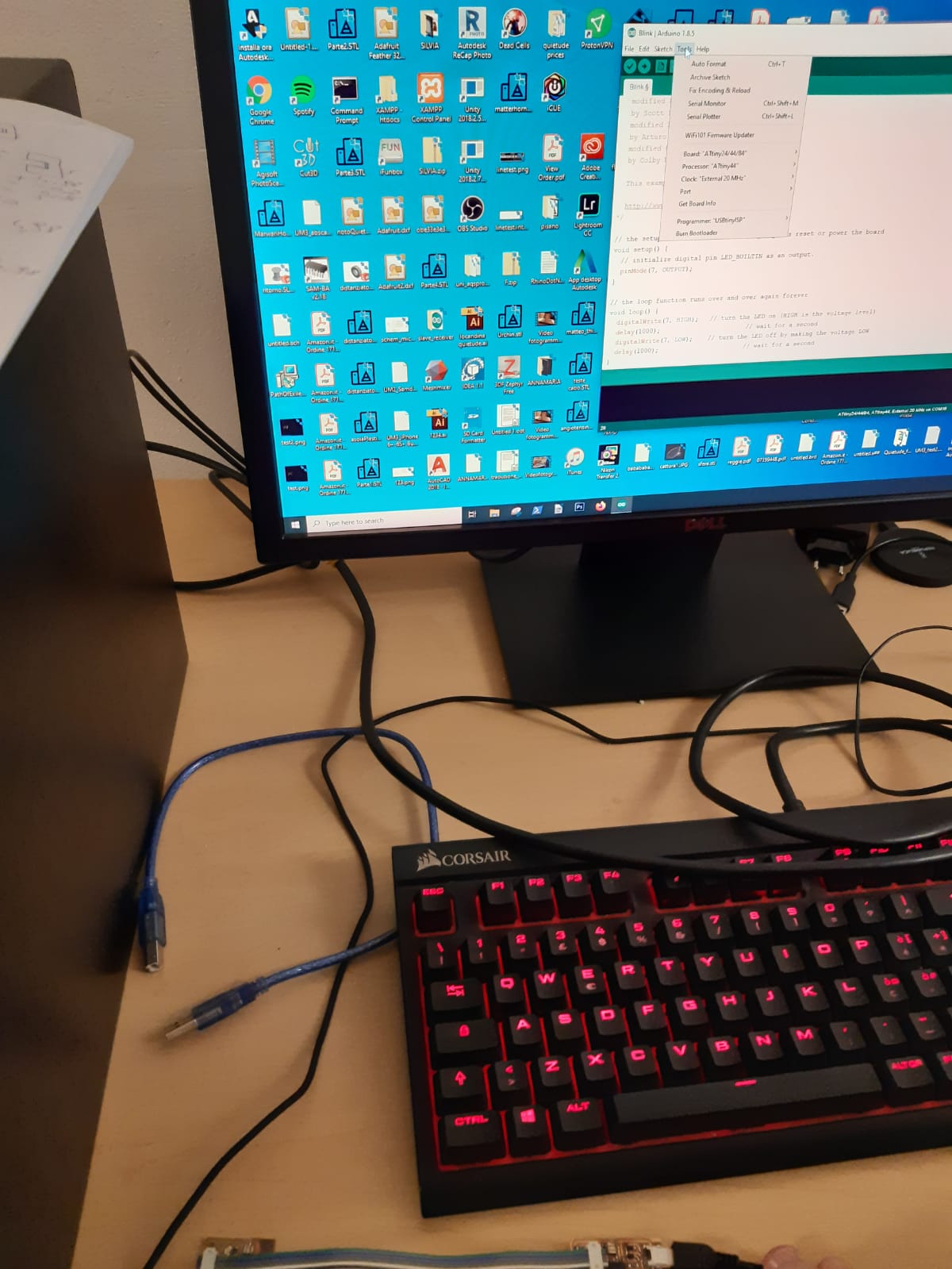
Once the pcb was recognized by the computer as usb tiny (which in itself gives no certainty of success), I verified that my programmer was working trying to program an arduino and with immense joy I discovered that it worked!!
You can find the downloadable files here
Outlines
Traces