6. Electronics design
Assignment
- Group assignment
- use the test equipment in your lab to observe the operation of a microcontroller circuit board
- Individual Assignments
- redraw the echo hello-world board
- add (at least) a button and LED (with current-limiting resistor)
- check the design rules, make it, and test it
- extra credit: simulate its operation
- extra credit: render it
Group Assignment
Check out the FabLab Kamakura site page
Individual Assignment
Components
I designed the board based on this example.
I decided to add an red LED and a tact switch to the ATtiny44 echo hello board.
Here are my components:
| Component | Specification | Number |
|---|---|---|
| micro controller | ATTiny 44 | 1 |
| resonator | 20MHz | 1 |
| capacitor | 1uF | 1 |
| resistor | 10KΩ | 2 |
| resistor | 499Ω | 1 |
| led | green | 1 |
| switch | tact | 1 |
| header | 6pin for FTDI | 1 |
| header | 6pin for ISP | 1 |
| resistor | 0Ω | 1 |
The 0Ω resistor was added later during my board design process. It is described in the following session.
Schematic Design
I used EAGLE to conduct the schematic and board design.
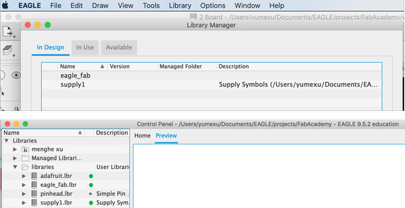
Firstly, I confirmed that eagle_fab library was activated (it was installed before FabAcademy started).
I opened Library > Library manager, and confirmed that it is there.
And in Control Panel, I confirmed that the green dot is on for eagle_fab library which means it is activated.
To add a component, click “add part” and search for the component. I made sure to conduct fuzzy search by putting asterisks to the keyword since the naming can be different. In the results, I chose the ones from eagle_fab library. (Eagle_fab library has the components from Fab inventory, having the library installed makes it easy to find the right component for circuit drawing.)
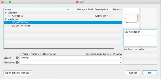
When I couldn’t find the components, I went through the whole list in eagle_fab library to find it. If there are multiple ones in eagle_fab library, I went for the ones with FAB in the names. (Again, because those are the ones in the inventory. So it makes sure that I choose the correct component since there can be other forms of a single component with different pads etc.)
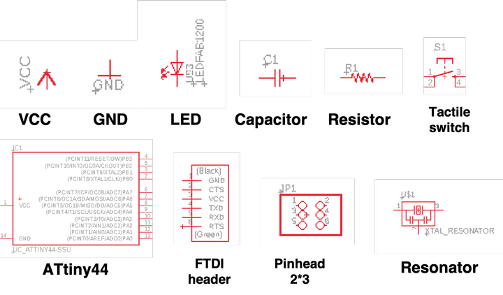
These are the components I used for schematic design first.
I connected the components as following using “Net” command. The rules for connecting are to:
- have VCC always pointing upwards, GND downwards(so current goes from the top to the bottom).
- have signal going from left to right
By the way, I typed in the name of the command to initiate the command, that’s the style of shortcut that EAGLE has.
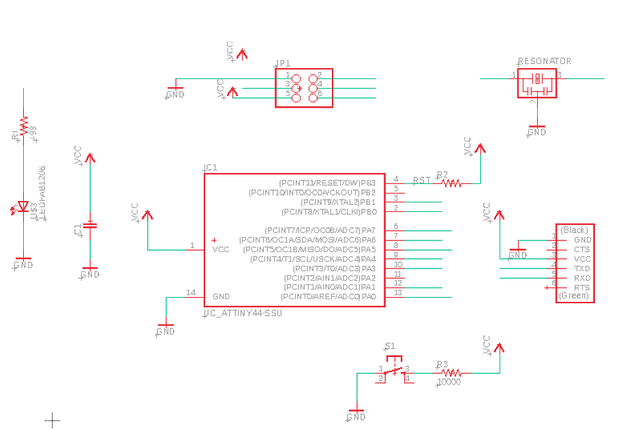
After connecting, I used ERC (Electrical Rule Check) to confirm if there is any misconnection.
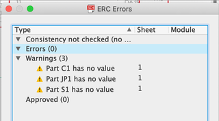
There were warnings but none of them seem fatal. (Warnings might be less fatal than errors in general.)
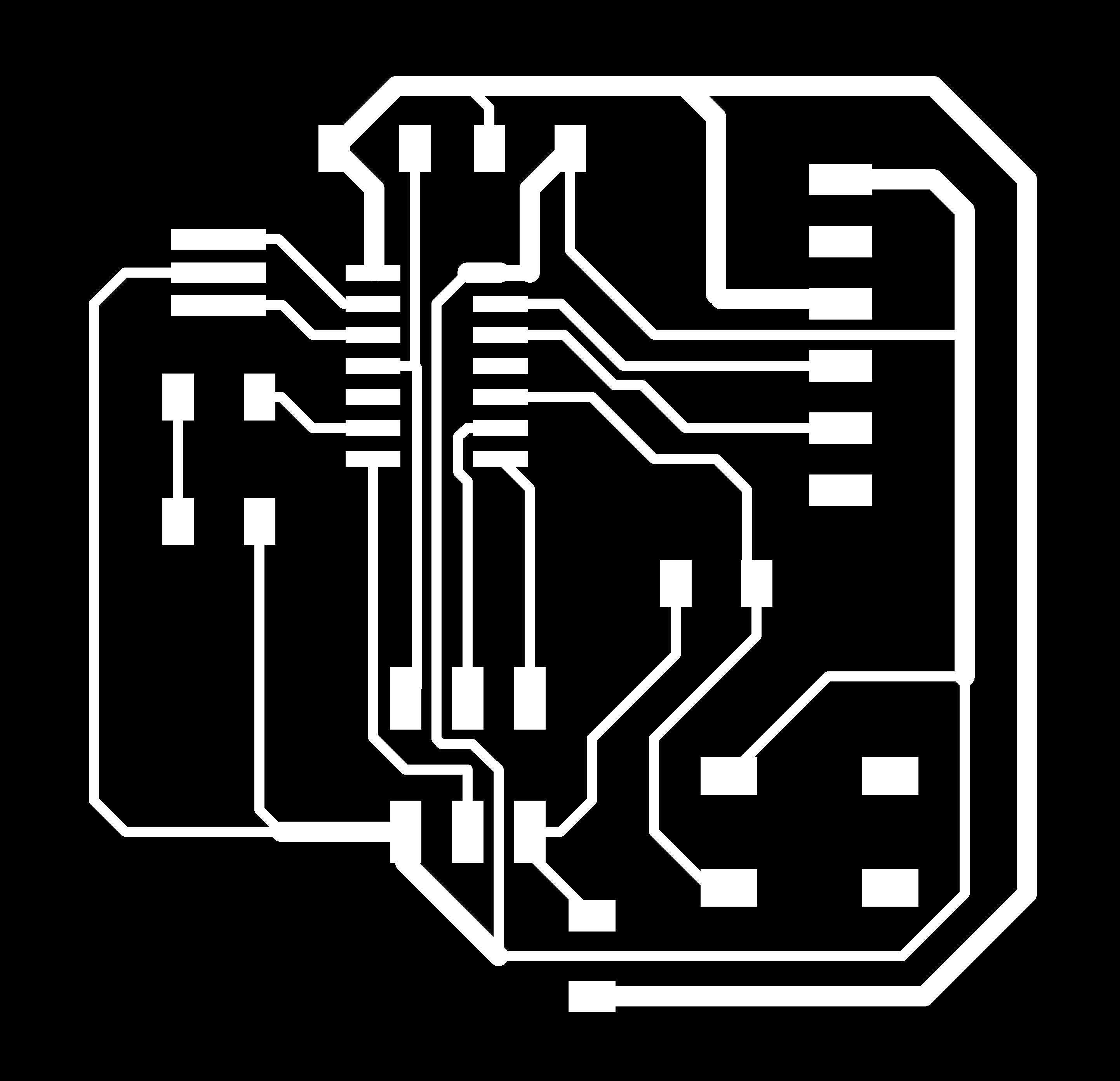
Board Design
Traces
Then I switched to board design (BRD).
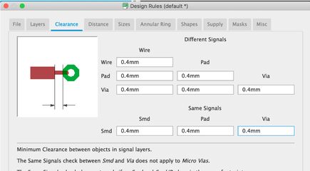
First I started with setting the design rules (View > Design rules).
Design rules are sets of rules for things like spacing between board features and minimum sizes that all correspond to the tolerances and capabilities of a board manufacturer. Setting these design rules will help you design your board in a way that will fit the requirements of board production (especially for the CNC machine).
I set all the minimum size for parameters in Clearance to 4mm. The mill I’m using for traces is 1/64 inch which is around 4mm.
Then I set up the grid.
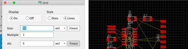
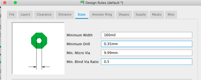
When I set up the size for the width, I made a mistake calculating the digit and I put 160mil (supposed to be 16mil, which is approximately 1/64 inch).
The line was drawn very thick, even if I tried to change the width by Change > Width to smaller sizes, it remained thick.
At that point, I recognized that the design rules define the minimum size of parameters, so even if I set a parameters to a smaller number, it still prioritizes the design rules.
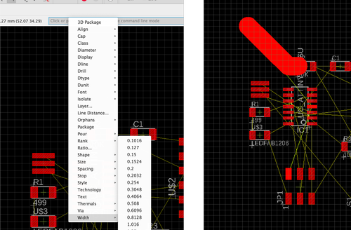
So I changed the minimum size of width and width to 15.5 mil in design rules and then it worked fine.
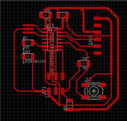
I tried to arrange and connect all the components by using command “move”, “rotate”, “route”, “ripup”.
I followed the advice of always using corners with 45 degrees instead of 90 degrees. The reason seems to be that electrons bunch up on the corners which is not preferable. (reference)
However, after hours of attempt, I just couldn’t route R3 properly…
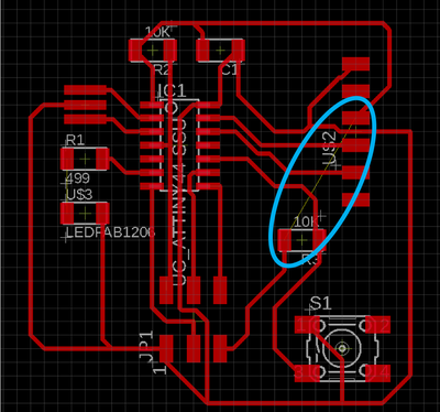
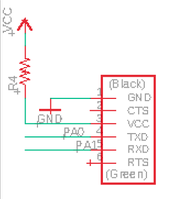
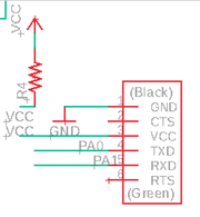
So I decided to add a jumper (0Ohm resistor, the space under it allows another path to go through) in between VCC and the VCC pin of US2.
I added R4 which is 0Ohm between VCC and VCC pin of US2.
However, when I went back to board design, it asked me to connect R2 with R3. In the schematics design, they both are connected to VCC, but not necessarily connected to each other.
I discovered that, if I connect R4 directly to VCC, EAGLE will think that R4 is the only component that is allowed to connect with VCC. So I changed the schematic design to this:
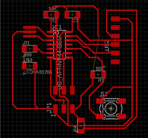
Then I was able to draw as I planned.
I followed the advice from instructors to make the traces coming from VCC and GND fatter.
The reasons stated by the instructors are:
“Thinner traces means more electrical resistance, which results in heat, especially when higher voltages are being used in the circuit.
Thinner traces might also cause more noise in the circuit, especially when the power lines (VCC and GND) are too long, and wrapped around the board.
For the low voltage circuits we are making (5V or less), fatter traces are technically not necessary.
However, fatter traces have another practical benefit. they are more robust and less prone to breaking. Moreover, fatter power traces means it is easier to distinguish them from signal traces when you have to debug.
Unless space is an issue, fatter power traces should be beneficial.”
So I changed width of several traces that’s directly connected to VCC or GND to 32 mil (I doubled the size).
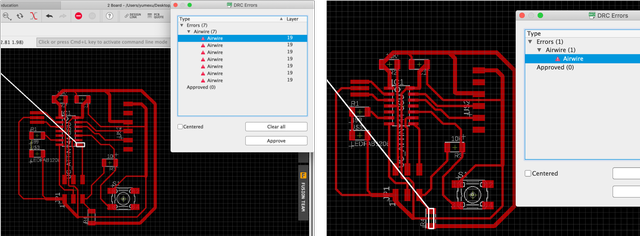
When I conducted DRC, it found some airwires. I tried to connect them again to make sure that the trace starts from and ends at the center of the component’s pad. The airwire shown between the 2 pads of R4 is not an airwire so I removed that Airwire warning message.
Outline
To make the outline, I switched to layer “48 document”. I used the “Polygon” command to draw a square that is bigger than the size of traces area.
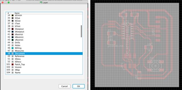
Then I changed the size of the yellow square.
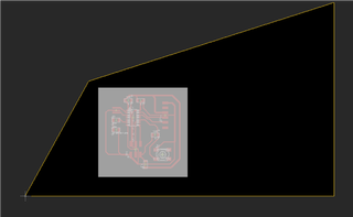
At first, I set the yellow square inside the square I drew in layer 48. When I exported it, I got a completely white square. I learned that the yellow square should be outside of the one in layer 48.
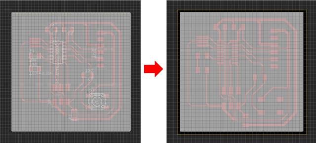
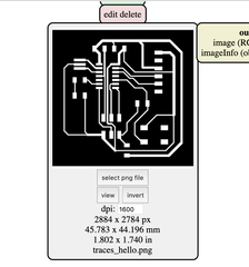
To export, only enable the layer of the trace or the outline, and choose monochrome with resolution of 800dpi.
At first I made a mistake by including other layers, so when I exported the traces file, it always came with an outline. When I disabled all other layers, it exported only the desired traces.
Board production
I used SRM-20 to mill the board.
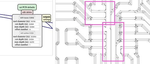
Using MODS, I imported the png files of both traces and outline png data with 1/64 mil and 1/32 mil.
Note that with Retina displays, there seem to be a bug that it creates files that are twice of the size as it is supposed to be. So I changed the resolution to half (800 to 1600dpi).
I milled the board, finding out that some traces that were not supposed to be connected were connected.
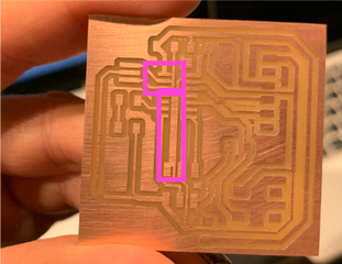
I recognized that I should check the toolpath generated on MODS before cutting. If I looked, I would have seen there wasn’t lines for those unexpectedly connected areas.
A way to solve it is to lower the size of mill on MODS so it can create path that once was considered not wide enough to go in between.
I changed the mill size from 0.0156 inches to 0.014 inches, and confirmed that cutting traces were generated properly.
It is basically “tricking” MODS to think that the mill is thinner, so caution is needed when doing that, since overdoing it might cause other problems.
I somehow felt that the mill cuts deeper than last time. It was very easy to get rid of unecessary parts, yet the risk of taking off essential parts arise.
This might be because the mill passes pathes closer to each other this time, so it carves some places that are overlaping, making the carves deeper.
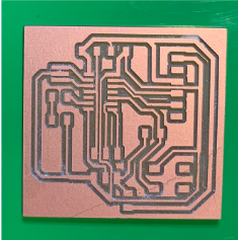
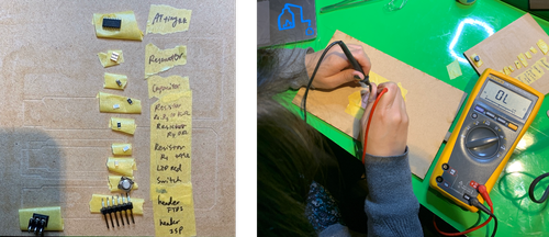
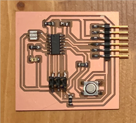
I soldered the components while checking the connections using multimeter.
Looking good!
Program
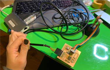
To program the board, I connected it with FabTinyISP, and to the computer using FTDI cable.
I downloaded the .c file and .c.make file, and cd to that folder through terminal.
I ran these 2 lines:
make -f hello.ftdi.44.echo.c.make
make -f hello.ftdi.44.echo.c.make program-usbtiny-fuses
And I disconnected the ISP, with the board connected to the laptop with the FTDI cable.
I ran this line:
make -f hello.ftdi.44.echo.c.make program-usbtiny
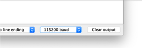
Then I opened Arduino IDE, selected port usbserial-AM005KE5E.
I opened serial monitor, changed the speed to 115200 baud.
When I typed something into the interface, it firstly echoed some garbled letters… I thought it’s because I just changed my system language from Japanese to English. So I restarted my laptop but the garbles remained.
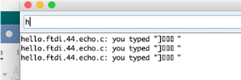
But the second morning, when I tried again, it turned out to be fine! “One byte at a time.”
When it didn’t work, I wonder if it was because the connection between FTDI cable and the board was not good.