7. Electronics design
Assignment
-
[x] group assignment: use the test equipment in the lab to observe the operation of a microcontroller circuit boards
-
[x] individual assignment: redraw the echo hello-world board, add at least a button and LED, check the design rules, make it and test it. Extra credit: simulate its operation and render it
Summary
Back to “my world”, but instead of using well-known tools as National Instruments Design Suite ( for schematic and layout) or Design Spark, I opted to use open-source software, namely KiCad, and to make a little bit more complex PCB.
Workflow is quite similar to other schematic and PCB layout programs, but strange issues with KiCad on Windows with the electrical rules checker, required a call to the Fabacademy team ( through issue tracker) slowed me down in the process....
Problem has been solved by editing the netlist manually. I then focused on the HelloBoard as originally proposed to complete the assignment…
Files are available here and here
Group assignment:
The minimum test equipment for a electronics lab consists generally in :
- regulated power supply
- low frequency generator
- oscilloscope
- logical analyzer
- multimeter
Resources available @FablabULB:
- HP 54602B oscilloscope, with HP 10071A 10:1 probes (attenuation ratio of 10:1: this means that the signal displayed on the screen is reduced by a factor 10)
- HAMEG Digital multimeter HM8011-3
As the lab is not completely equipped yet, we decided to go for simple measurements:
- Continuity check: with simple multimeter, we can check if there are shorts and no-contact on the nets (unpowered system).
- Diode check: with a simple multimeter, we can check if the diodes (Leds, Zener, signal, etc..) are polarized correctly (unpowered system)
- Voltage measurements: DC voltages at given points are easy to measure with a simple multimeter, AC voltages and time-varying signals are best measured with a oscilloscope…(powered system)
- Current measurements: more difficult to measure, as the loop where it flows needs to be opened....
We measure the signal on VCC pin: (either on the multimeter or the oscilloscope):
We measure the signal on the blinking led :
 |
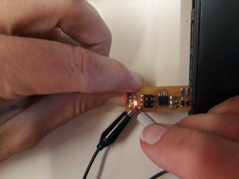 |
|---|---|
| programming | measuring |
To see the variations, we best use the oscilloscope:
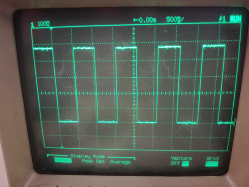
We recognize the 1sec period (scale is 500msec/square), and the attenuation factor of 10 (scale is 100mV/square)
Individual assignment:
Notes and Introduction
After making and programming a simple embedded system, starting from a given layout and program (week5 assignment), we’re going to design a embedded system, that we will have to program later ( week9 assignment)
The minimum required is to redraw the echo hello-world board, add at least a button (input) and LED (output).
I decide to use the open source Kicad EDA software.
In the electronic process, we first have to define the functionality of our board, developing a schematic circuit, that will represents the structure/diagram of our system, thanks to logical models of the real components, connected through wires.
Simultaneously, KiCad, as any good EDA, has different footprints associated to the logical components, in order to prepare the layout of the PCB.
And that will be the next step: creating the layout of the PCB. The challenge here will be to place the components - even making the footprint if is is not included in the library - and route the nets into a realistic and proper PCB…
Last but not least, 3D rendering of the results and simulation of the whole system helps have nice presentations and good understanding!!
Download and Install KiCad
Download KiCad for Windows from here.
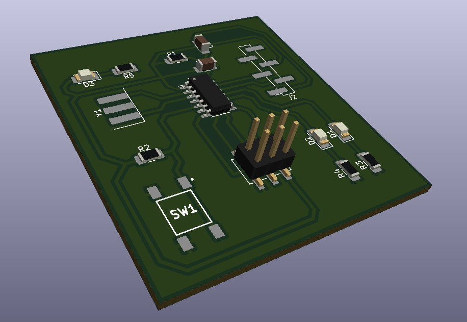
Looking at the hello-world board, we can see that it includes a ATtiny44 microcontroller, with its external quartz resonator (quartz + associated capacitors included), a decoupling capacitor of 1µF, a pull-up resistor of 10k, an ICSP Header J1 and a serial communication J2 (FTDI Header).
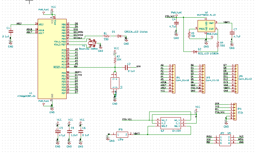
Let’s do something similar with a ATMEGA328P, creating something similar to an ARDUINO NANO....
The functionality we want to add: * Lipo battery (best 2500mAh) and charge management controller MCP73831 OR linear regulator allowing power supply from the wall… * Analog and Digital outputs/inputs available to outside world through pin headers * ICSPHeader * Serial connection to PC through the SparkFun FTDI Basic Breakout - 3.3V-5V, that convert the USB signal into a serial signal TTL level RX/TX and vice-versa.
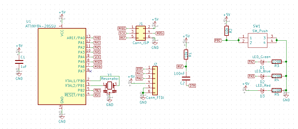
Having issue with the creation of the PCB for this board ( see below), we decided to also use a simple “Helloboard”, just adding a pushbutton and three leds on the original hello-world-board, as illustrated below.
So, let’s start to use KiCad....
KiCad is a suite of several tools, specialized in given tasks:
* KiCad: Project manager
Eeschema: Schematic editor and component editor
Pcbnew: Circuit board layout editor and footprint editor
* GerbView: Gerber viewer.
First of all, create a new project: File → New → Project. Give a name to the project file. The project file will automatically take the extension “.pro”
A comprehensive list of tutorials and manuals can be found here.
PCB design
STEP 1 : Create a schematic
The first task is to launch the Eeschema tool, clicking on the Eeschema icon
, and to create a schematics.
This is done with the help of schematics symbols (passive components, microcontrollers, connectors, etc), which are put in connection through wires.
Great help on eeschema is available here.
Next,click on the ‘Page Settings’ icon
on the top toolbar, to set the appropriate ‘paper size’ and enter the title.This information will populate the schematic sheet at the bottom right corner. Save the whole schematic:
File → SavePlace the components: Click on the symbol library editor icon
in the toolbar. Or press the ‘Add Symbol’ hotkey [a], click on the middle of the schematic sheet. A window will appear on the screen, which enables to choose the symbol.
Beside the official, integrated symbols library (that may be regularly updated from here), accessible through the library editor icon ![]() , other libraries can be added, as global or specific to the project (In the Library Editor:
, other libraries can be added, as global or specific to the project (In the Library Editor: Preferences → Manage Symbol Libraries).
The library loader program, provided by Samacsys and available here is also available on the on line distributors sites as RS or Mouser. It makes the integration of new schematics symbols and footprints into the KiCad libraries quite easy, avoiding the tedious task of creating manually a symbol and a footprint for new components…
Here are the steps to follow to integrate the Samacsys parts into the KiCad libraries.
And finally, it is still possible to create our own schematic symbols and footprints in the library editors…
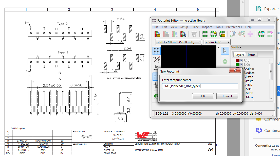
Just be careful: there are the legacy format (.mod) and the new libraries format (.pretty), and new symbols and footprints can not be added to the legacy format libraries…
It is a good habit to check if the footprint for the chosen symbol already exist in the footprint library, at the time of the incorporation of the symbol in the schematic.
Repeat the add-component steps, creating new symbols and footprints if required, and organize all components on the schematic sheet. All components need to have unique identifiers. If not done manually , identifier assignation can be done automatically by clicking on the ‘Annotate schematic symbols’ icon
on the top toolbar.
To move the components around and make the connections, useful hotkeys are available (see list in eeschema help).
Next, wire all the components as required. An alternative way of making a connection is to use labels. This is a useful technique when connecting wires in a complex design where drawing the lines would make the whole schematic messier.
To place a label you do not necessarily need a wire, you can simply attach the label to a pin. Just be sure to anchor the label, that is still an independent item, exactly on a wire or a pin for the label to take effect.
Labels somewhere in the schematics, having the same name, create an invisible connection between the related pins/wires.
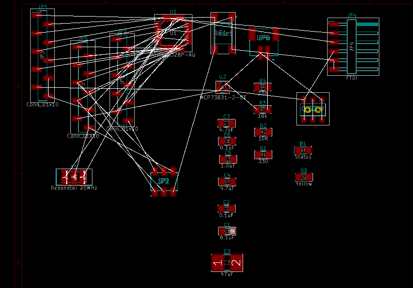
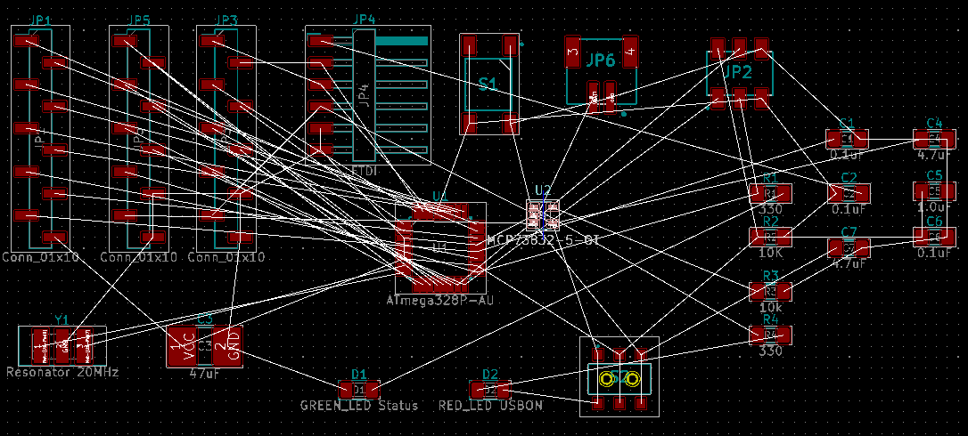
Here are the schematics of our boards.
The ATmega328 board:
The ATtiny84 board:
Check the schematic for errors. Click on the ‘Perform electrical rules check’ icon
on the top toolbar.
FAILED!! I still get some errors and warnings for the ATmega328 board, for which I don’t see a way out....e.g. the classic schematic checking errors: “Pin not connected” ( eg DTR, or pin1 of battery management chip) or “Pin connected to some other pins but no pin to drive it” still appears. The latest error can be repaired by adding a general powerflag to the concerned net/pin, AND adding a VCC and GND labels on every related wire…
For the ATtiny84 board, everything goes smoothly…
Check the footprints assignation to components and create netlists:
Tools → Update PCB from Schematic. Let us not forget that we have to assign footprints to symbols first. Cvpcballows us to link all the components in our schematic with footprints in the KiCad library.
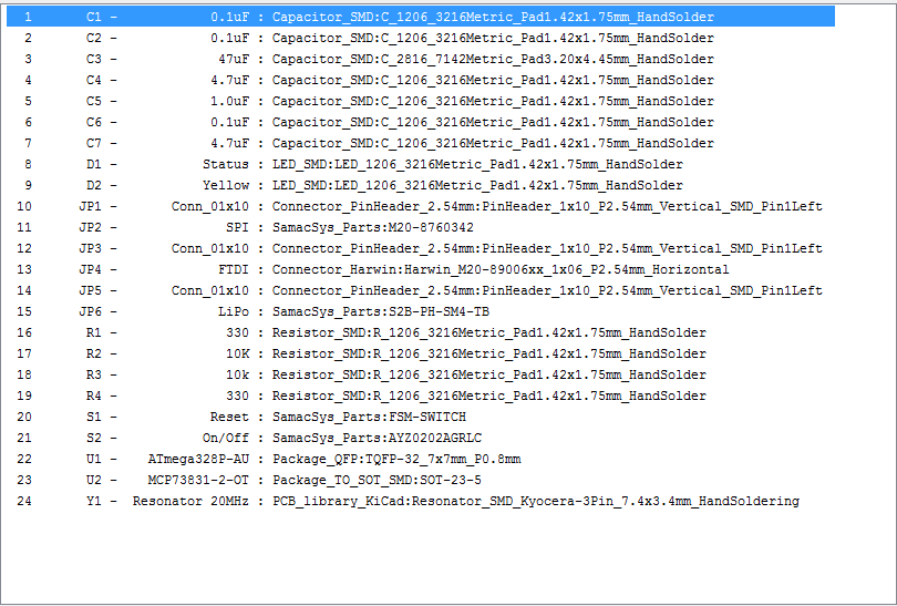
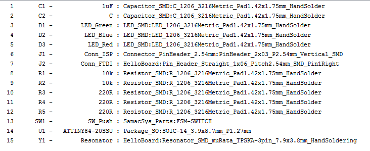
Here are all components used in our schematics:
The ATmega328 board:
The ATtiny84 board:
The netlist is a “simple” text file indicating the components and the connections between them in the schematic. This netlist will be used in the layout process to ensure the correct connections, by visualisation of ratsnest, showing the connections while we are routing
The point here is that the netlist will not be complete as long as the ERC is not OK!!!
STEP2: Create the PCB layout
The next task is to launch the Pcbnew tool, clicking on the pcb layout editor icon
, and to create a PCB layout. If we’ve used the command
Tools → Update PCB from Schematic, the components and the ratsnest are shown:
And effectively, we got an incomplete routing when making the PCB: FAILED!
Issue has been added on issues tracker…
Without response on the issue, I edited the netlist manually, and got the complete ratsnest: netlist completed!
In Pcbnew, we now start the PCB from the netlist directly: Tools → Load Netlist
Helloboard
For the ATtiny84 board, everything goes smoothly again. Due to a lack of time, I decided to leave the ATmega328 board for the next assignments, and to go further with the Helloboard this week…
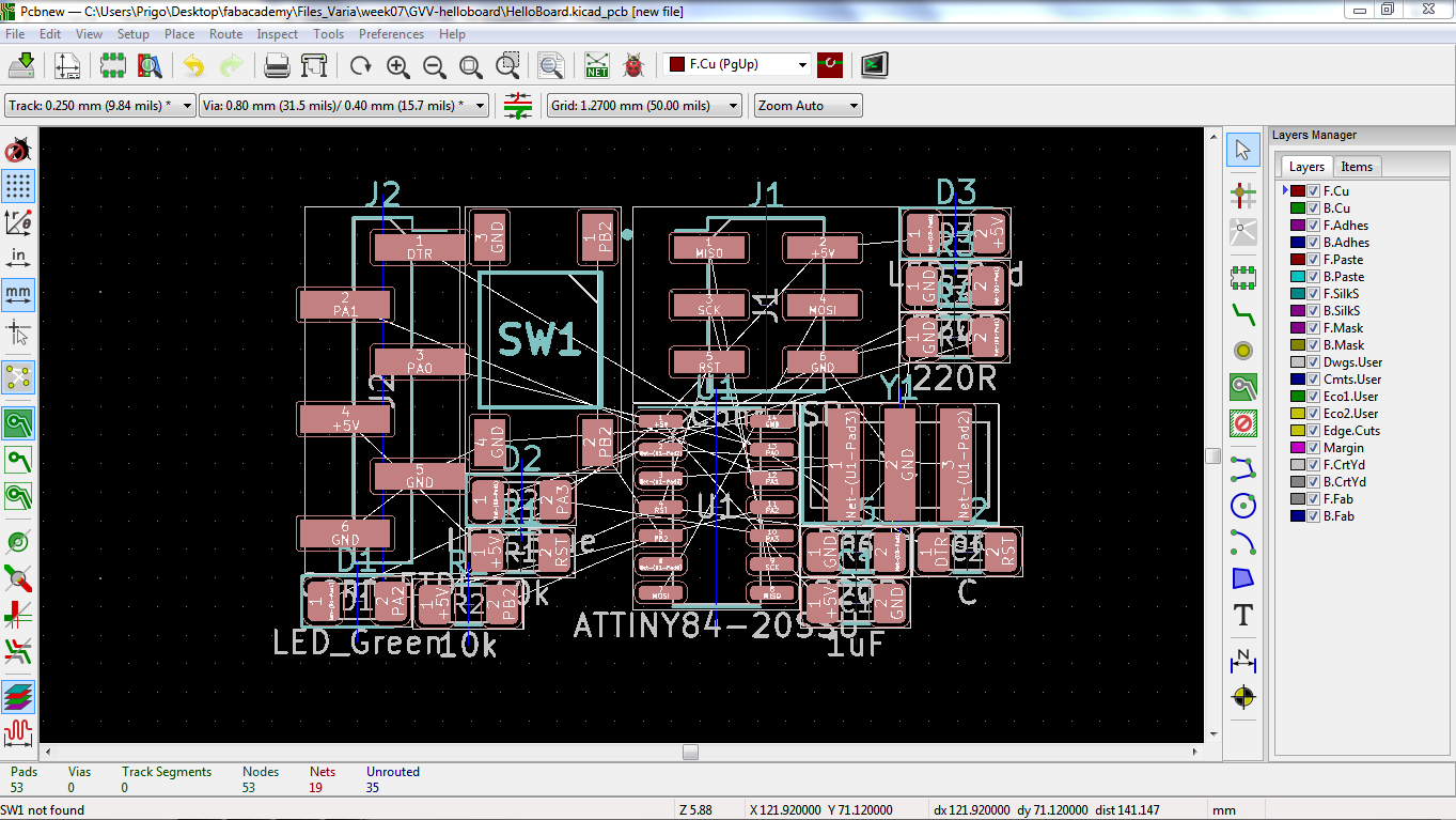
The first step is to separate the components, moving them around, rotating them in order to get a global picture where the ratsnest are not crossing to much each other, in order to facilitate the routing process, surely when using one layer PCB, without way out to another copper layer for easy routing…
Define the design rules prior to start routing, in
Setup → Design rules → Global Design Rules. We use the results of week5 for our milling machine: * clearance of 0.4mm
* track width minimum of 0.4mm, let’s use 0.5mmStart routing, using the route tracks icon
, on the correct layer! (front copper for single face PCB, front and back layer for double face PCB)
This process may require to move and rotate the components again to get some feasible routing on one layer…
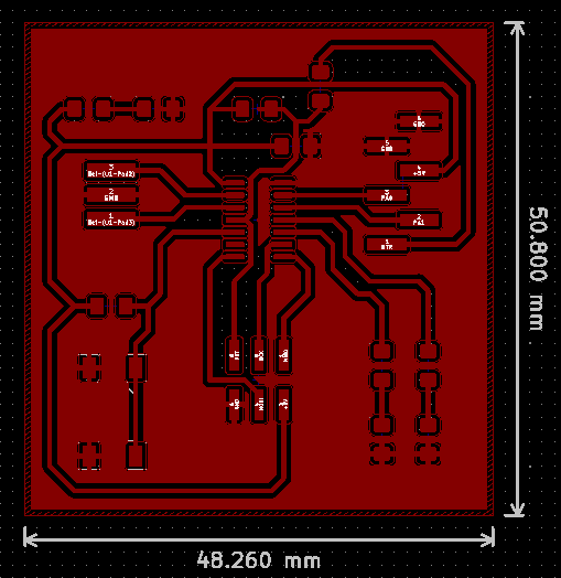
We route all nets, except the GND, for which we create a ground plane, that will be connected to all GND pins, with the tool ‘Add filled zones’![]() on the right toolbar.
on the right toolbar.
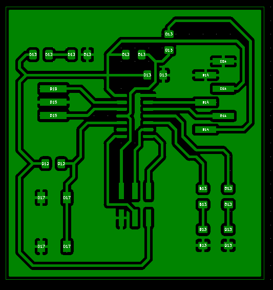
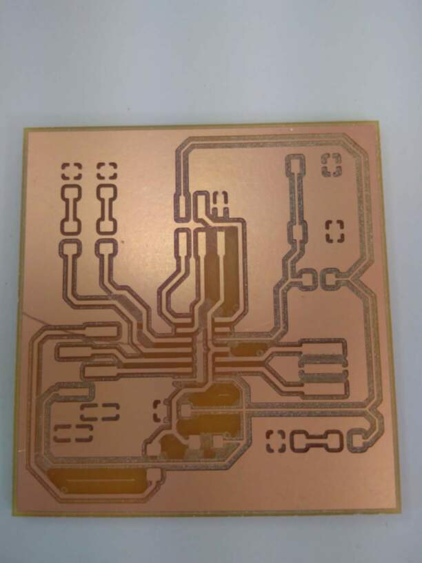
Here is the result for the ATtiny84 board:
Click on the ‘Perform design rules check’ icon
Save the file by clicking on
File → Save. To admire your board in 3D, click onView → 3D Viewer
In order to have all data related to the design in one unique directory, with the final version of the PCB,
- we rename the Helloboard_cache.lib into Helloboard.lib: this file contains all the symbols used in the design
- we save the footprints locally through:
File → Archive Footprints →Archive Footprints in Existing Libraryand choose Helloboard: this will create a Helloboard.pretty, containing all the footprints used in the design…
To render a 3D view of the assembled PCB, we first need to download the 3D packages from Github here, check that the KISYS3DMOD parameter points to the correct folder containing the 3D packages. Components done manually or through the Library loader program do not include 3D shapes. We could - but didn’t - modify the component symbol/footprint file to include some FreeCAD *.step files to render the component… Here is the partial 3D view (without the resonator, push button and FTDI connector):
STEP 3 : Generate the gerber File**
Once the PCB is complete, we can generate Gerber files for each layer (only one for the ATtiny84 board) with the command from the top toolbar: File → Plot.
Preview the Gerber File with the tool GerbView in the KiCad manager.
We first print the PCB layout on paper to check the dimensions of the pads against the real components:
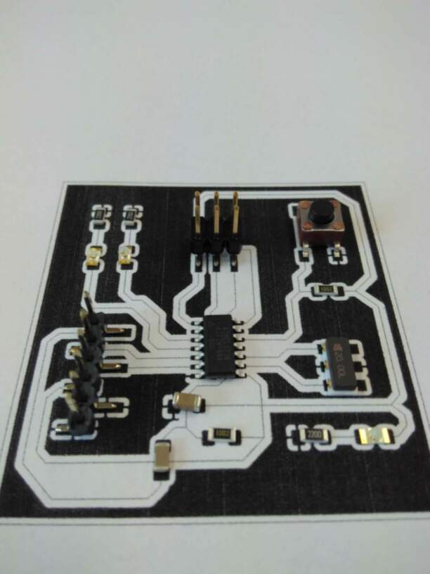
Pads are OK! (the traces are not, but this is due to the PDFcreator printer, and is of no importance here…)
All the files related to the design of my HelloBoard are found here and here.
PCB fabrication
Next step is to mill the PCB on the Bantam machine. As described in week5, calibration of the bantam machine has to be realized before the real milling process itself:
- Homing: to locate the start position ( zero coordinates)
- Locate tool: to determine the height of the tool in the grips.
- Height of the PCB: in the menu (
bitbreaker → probe material), to determine the height of the PCB.
Do not forget to define the material type ( Single-sided FR1).
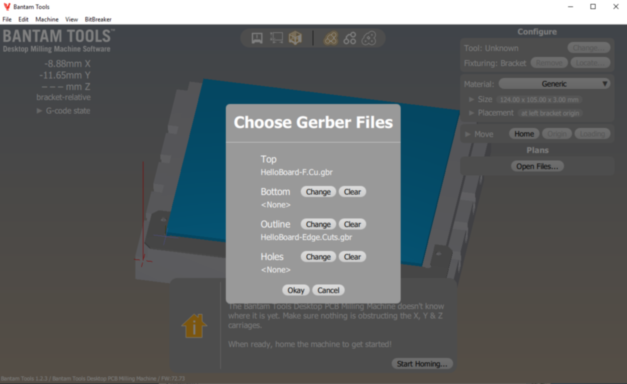
We then load the gerber files (File → Open Files), defining which gerber is used for the top layer and the outline:
We choose the tools to be used int the process, the machine defining the order itself, depending on the work to be done :
- Flat end 1/64
- Flat end 1/32
- Flat end 1/16
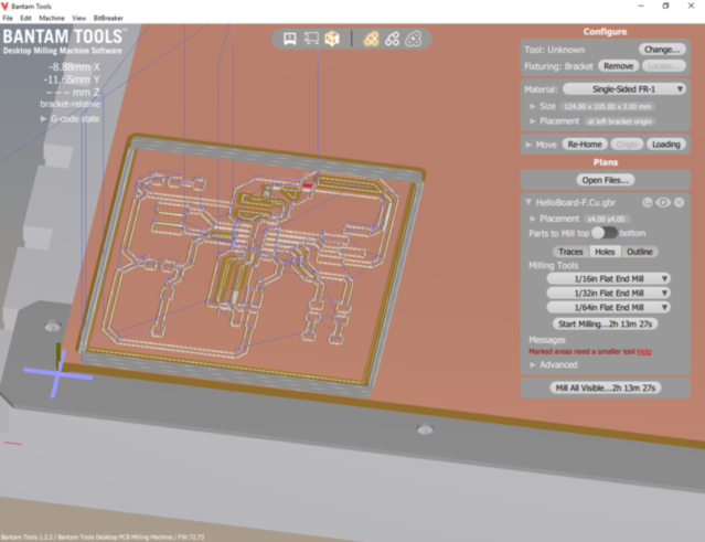
The process takes too much time! (2h). Moreover, there is a point where the milling will not be achieved correctly (message in red: marked area need a smaller tool).
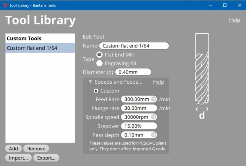
So we decided to create a new tool, custom flat end 1/64, with a higher spindle speed (File → Tool Library):
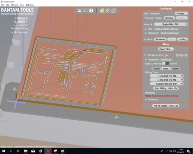
Yeah! This reduces the process time by a factor two:
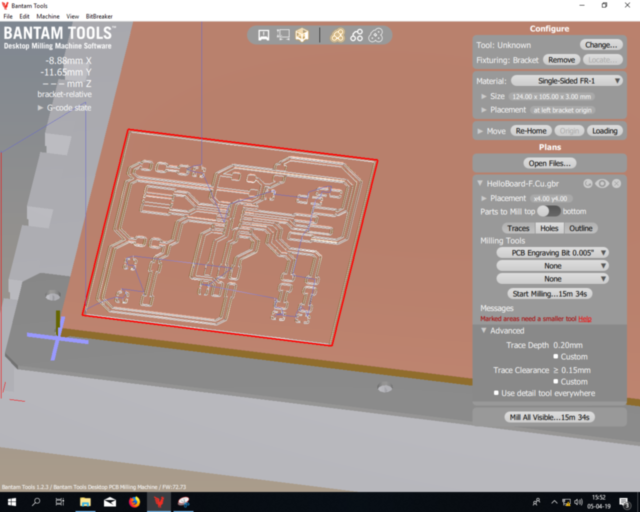
And to complete the job, we add a last pass with a PCB Bit Engraving tool 0.005”
The result is illustrated here:
Potential issue: three traces to the ATtiny pins (1, 5 and 14 ) are narrower than the others…
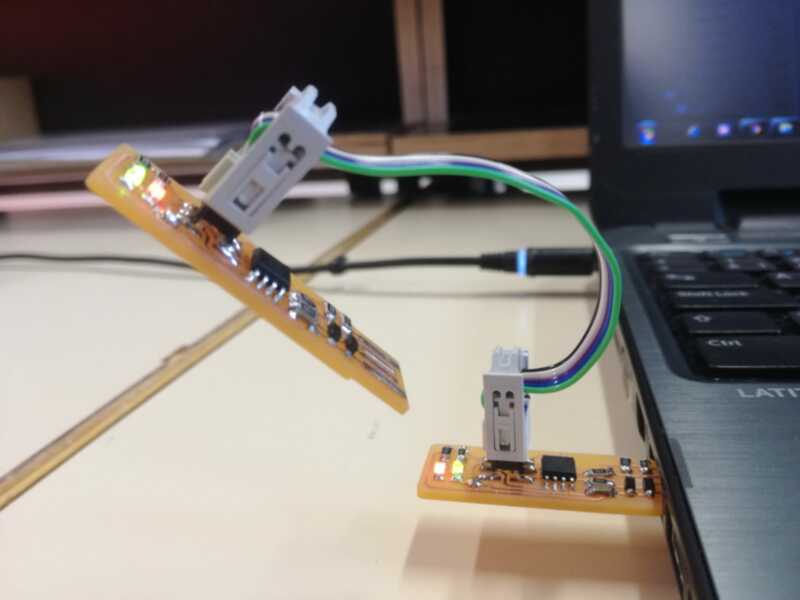
PCB assembly and testing
Nexts steps are assembly and hardware testing, as described in week05: * Assembly of the components, starting with the smaller ones, and finishing with the SPI and FTDI connectors, taking care of the orientation of components. * Hardware tests to verify the quality of the system.
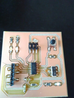
Everything seems fine!
Programming
The objective is now to establish a communication between our board and a PC, through the FTDI connector pins RX and TX, loading the hello.ftdi.echo.c program
Other versions of the program, using the interrupt functions can be tested as well: here. An assembler version is also available here
Let’s try the simple “hello” program first. The original hello.ftdi.44.echo.c file doesn’t need adaptation, as there are no differences concerning the pinout of an Attiny84 (8kb of flash memory, SRAM of 512kb) and an ATtiny44 (4kb of flash memory, SRAM of 256kb).
Some adaptation of the original MAKE program is needed to adapt it to a ATtiny84 with WinAVR:
PROJECT=hello.ftdi.84.echo
SOURCES=$(PROJECT).c
MMCU=attiny84
F_CPU = 20000000

CFLAGS=-mmcu=$(MMCU) -Wall -Os -DF_CPU=$(F_CPU)

all: $(PROJECT).hex

clean:
    rm -f usbdrv/*.o
    rm -f *.hex *.elf *.o

$(PROJECT).hex: $(PROJECT).out
    avr-objcopy -O ihex $(PROJECT).out $(PROJECT).c.hex;\
    avr-size --mcu=$(MMCU) --format=avr $(PROJECT).out

$(PROJECT).out: $(SOURCES)
    avr-gcc $(CFLAGS) -I./ -o $(PROJECT).out $(SOURCES)

# program-usbtiny:
program : $(PROJECT).hex
    avrdude -p t84 -P usb -c usbtiny -U flash:w:$(PROJECT).c.hex

#program-usbtiny-fuses:
fuses : $(PROJECT).hex
    avrdude -p t84 -P usb -c usbtiny -U lfuse:w:0x5E:m
Using a external resonator of 20MHz requires to adapt the fuses accordingly: this is the value of the low byte fuse. Here, we set them as follows: 0x5E
From the ATtiny24-44-84 datasheet: * CKSEL3:CKSEL1 = 111 selection of an external resonator with frequency range greater than 8MHz, * SUT1:SUT0 = 01, with CKSEL0 = 0 sets the Start-up Time from Power-down of 258CK and an additional delay of 14CK+60ms, Recommended Usage for Ceramic resonator, slowly rising power from Reset
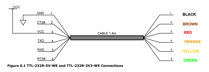
To ensure the power supply of the board AND communication with the PC through the FTDI connector, we build the cable from a FTDI cable TTL-232R-5V-WE, with the correct conections:
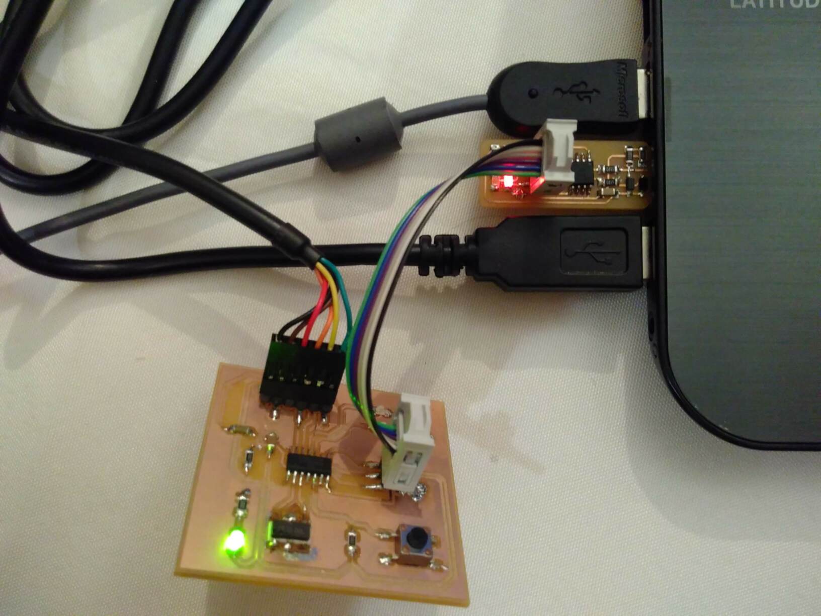
I use my programmer to program my Hello board ( it works from the first time).
Here is the hardware setup:
In Programmer’snotepad ( WinAVR), let’s use make all to create the hex file, make program to load the program into the ATtiny84 and make fuses to program the clock fuses properly…
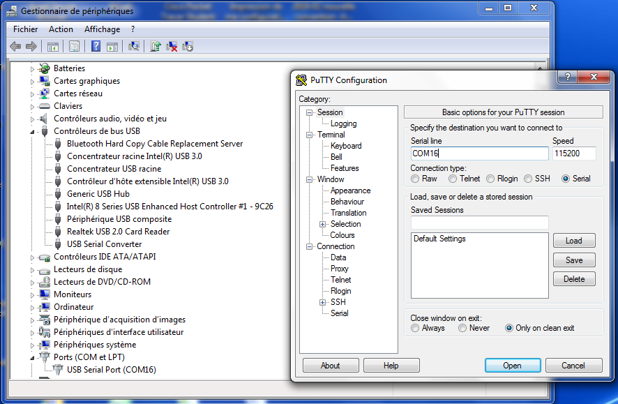
I install PuTTY on my PC, use it in serial mode, with port COM16 (check the port in Devices manager when FTDI cable is connected to the PC) and baudrate 115200 :
Great, here we have!!
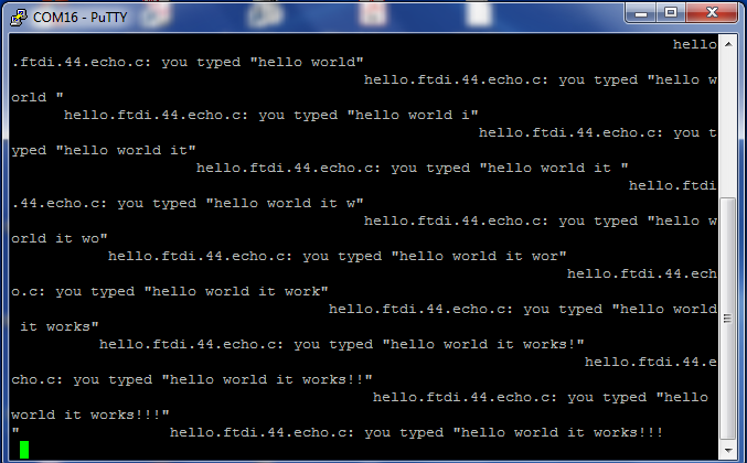
Well, let’s add a carriage return (ASCII code 13 in decimal) in the hello.ftdi.84.echo.c program, before the line feed (ASCII code 10 in decimal):
put_char(&serial_port, serial_pin_out, 13); // carriage return
put_char(&serial_port, serial_pin_out, 10); // new line
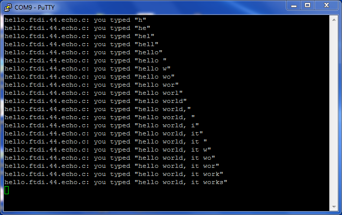
I also tried the interrupt version, where all the process is managed by an interrupt service routine (ISR), providing the same results....
All the files related to the programming of my HelloBoard are found here.
Still to do if I had time....
-
Create an 3D model of the connectors in FreeCAD.
-
Use the assembler version of the HelloBoard…