Week 10: Output devices & power measurement
Output devices week. Our group measured output power on the bench (below). For my individual assignment I programmed outputs on two boards I designed: on the WROOM display PCB (board #2) a 2.4″ ST7789 colour TFT over SPI, its backlight (BL) over GPIO, and an I²S speaker through a MAX98357 amplifier; on the charging dock (board #3) a 1602 I²C LCD that shows charge voltage, current, power, and duration (§7). Sensor data reaches the WROOM over HostLink I²C from the XIAO hub (board #1, Week 8); the TFT harness runs pot → base → WROOM pads (§4). Neither board is an off-the-shelf dev kit (§2).
Individual assignment: outputs on WROOM PCB & charging dock
The Output Devices assignment asks me to add and program output devices on a board I designed. I used two of my own boards: board #2 drives ST7789 pixels, the TFT backlight, and speaker audio; board #3 drives the dock 1602 LCD. I also kept the pin names, connection diagrams, and source links on this page because those were the parts I needed to re-check during integration.
1. Task and motivation
Week 9 reads light, RH, and temperature on hub
board #1 (Week 9). Output week adds a colour face on
board #2: the WROOM firmware receives an 8-byte TelemetryPacked HostLink frame
(cmd 0x01, slave 0x55) from the XIAO hub, paints the ST7789 over SPI, and
switches the panel backlight. The same WROOM output board also drives the front speaker with I²S audio in the
integrated project. Splitting sense (hub) from show/sound (WROOM + TFT + speaker) matches the Forest Fairy
layout I kept through Week 11 and Week 15.
2. Designed PCB for Output Devices — WROOM display board (board #2)
Forest Fairy uses three PCBs I designed. Output Devices week focuses on board #2, the leaf-shaped carrier that hosts an ESP32‑S3 WROOM module, breaks out the ST7789 harness, and carries support circuits (power input, decoupling, pull-ups). Boards #1 and #2 could have been one layout, but the mobile base did not have room, so I split sensing (XIAO + Pico) from display (WROOM + TFT).
| Board | Role | Output week? |
|---|---|---|
| #1 Hub | Seeed XIAO ESP32-S3 + Pico/NanoStat sidecar; FPC J1 on this panel (Week 6/8) |
HostLink master only (sensors → I²C) |
| #2 WROOM display | ESP32‑S3 WROOM (U15) + screen wire pads + 5V/GND/3V3 header (U16) |
Assessed board — ST7789 + firmware |
| #3 Charging dock | Seeed XIAO RP2040 + 1602 I²C LCD + status LEDs; A2/A3 sense charge rail (Week 9) | Assessed board — LCD output + dock firmware |
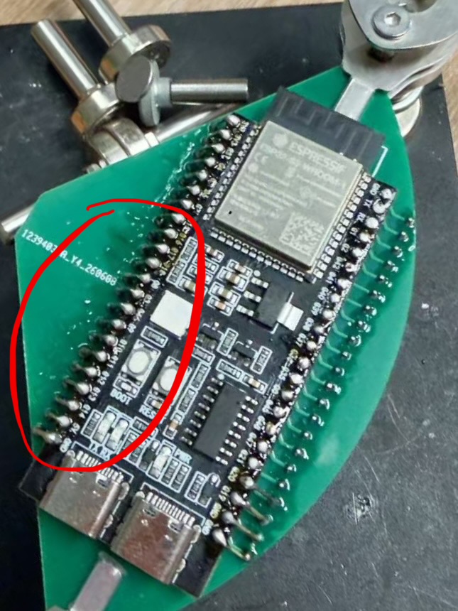
There is no FPC on board #2. The flex connector lives on the hub PCB (board #1) for other integration paths. On the WROOM board the TFT interface is a set of edge pads I routed in EasyEDA for the screen harness (highlighted in the layout export below). Mentor feedback asked for a PCB with TFT provisions; this landing pattern plus the pot→base wiring is that provision, not a commercial Arduino or generic ESP32 breakout.
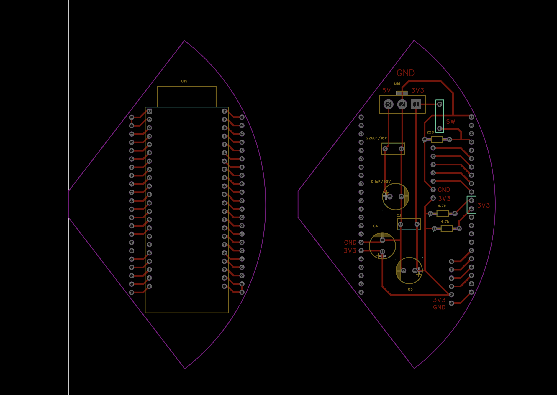
U15 ESP32‑WROOM footprint (left) and
populated circuit (right). Highlighted pad groups (layout markers) are where the ST7789 harness
lands — SPI/power nets fan out from the module to these edge pads before the wires continue to the pot-mounted
panel.
Design source:
design-files/week10/wroom-pcb.eprj2
(嘉立创 EasyEDA / JLC project). Hub KiCad for board #1 is on
Week 6 — HostLink context only, not the assessed Output Devices PCB.
3. What I had to learn first
The ST7789 wants a fast RGB565 SPI stream; the backlight BL pin is a separate GPIO I turn on
in setup() before any draw calls, or the panel stays dark even when SPI is fine.
The speaker path is I²S into a MAX98357, with GAIN and SD pins for
level and enable. Sensor numbers still arrive as an 8-byte HostLink frame
(magic 0xA5, cmd 0x01, RH, temp×10, light×10); the WROOM repaints
when dataVersion bumps. Group bench work this week (
below) also showed me how much current the TFT backlight can
pull compared with logic-only loads.
4. Output device A — ST7789 TFT (SPI)
Working principle
The ST7789 is a TFT LCD controller with an on-chip GRAM framebuffer. Unlike the OLED, it expects a high-speed 4-wire SPI stream of RGB565 (16-bit colour) pixels. The control lines are simple but easy to mix up: CS is the idle-high chip select, DC separates command bytes from pixel data, RST gives the panel a hardware reset pulse before init, BL enables the backlight through a GPIO, and SCK / MOSI carry the SPI clock and master-out data. MISO exists on some modules but is not part of my normal UI draw path.
After reset, Adafruit_ST7789::init() sends a vendor init sequence (sleep out, pixel format,
MADCTL rotation). Each fill or text call sets a column/row window, then streams 16-bit colour
words over SPI. Capacitive touch (FT6336) is a separate I²C device — not part of the SPI pixel bus
(documented further in Week 15).
Connection diagram — system level
flowchart LR
  Hub["Board 1: XIAO hub PCB
Week 8 — sensors + HostLink"]
  Wroom["Board 2: custom WROOM PCB
ESP32-S3 + screen pads"]
  Tft["ST7789 TFT in pot
320×240 RGB565"]
  Bl["Panel backlight BL
GPIO17"]
  Spk["Speaker output
MAX98357 + front speaker"]

  Hub -- "I2C 100 kHz
SDA D4/GPIO9
SCL D5/GPIO8" --> Wroom
  Wroom -- "SPI 26 MHz
SCK18 MOSI8 CS9
DC3 RST46" --> Tft
  Wroom -- "GPIO HIGH
BL17" --> Bl
  Wroom -- "I2S audio
LRCK42 BCLK41 DIN40
GAIN39 SD38" --> Spk
board_pins.h.
ST7789 pin map (WROOM → panel)
| Signal | WROOM GPIO | Role in firmware |
|---|---|---|
| SPI SCK | 18 | SPI.begin(18, 16, 8) clock |
| SPI MOSI | 8 | RGB565 pixel stream to panel |
| SPI MISO | 16 | optional readback (unused in UI draw) |
| TFT CS | 9 | Adafruit_ST7789(Pins::TFT_CS, …) |
| TFT DC | 3 | command vs data select |
| TFT RST | 46 | hardware reset before init() |
| Backlight BL | 17 | backlightSet(true) in setup |
| HostLink SDA | 37 | I²C slave Wire1, addr 0x55 |
| HostLink SCL | 36 | receives TelemetryPacked from hub |
Pin constants live in
code/week10-i2c-env/wroom/src/board_pins.h
(same map as
final-project board_pins.h).
Screen harness — pot → base → WROOM PCB
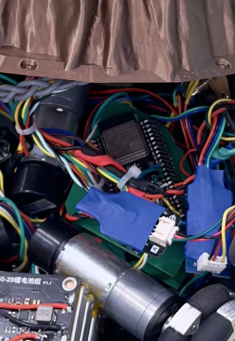
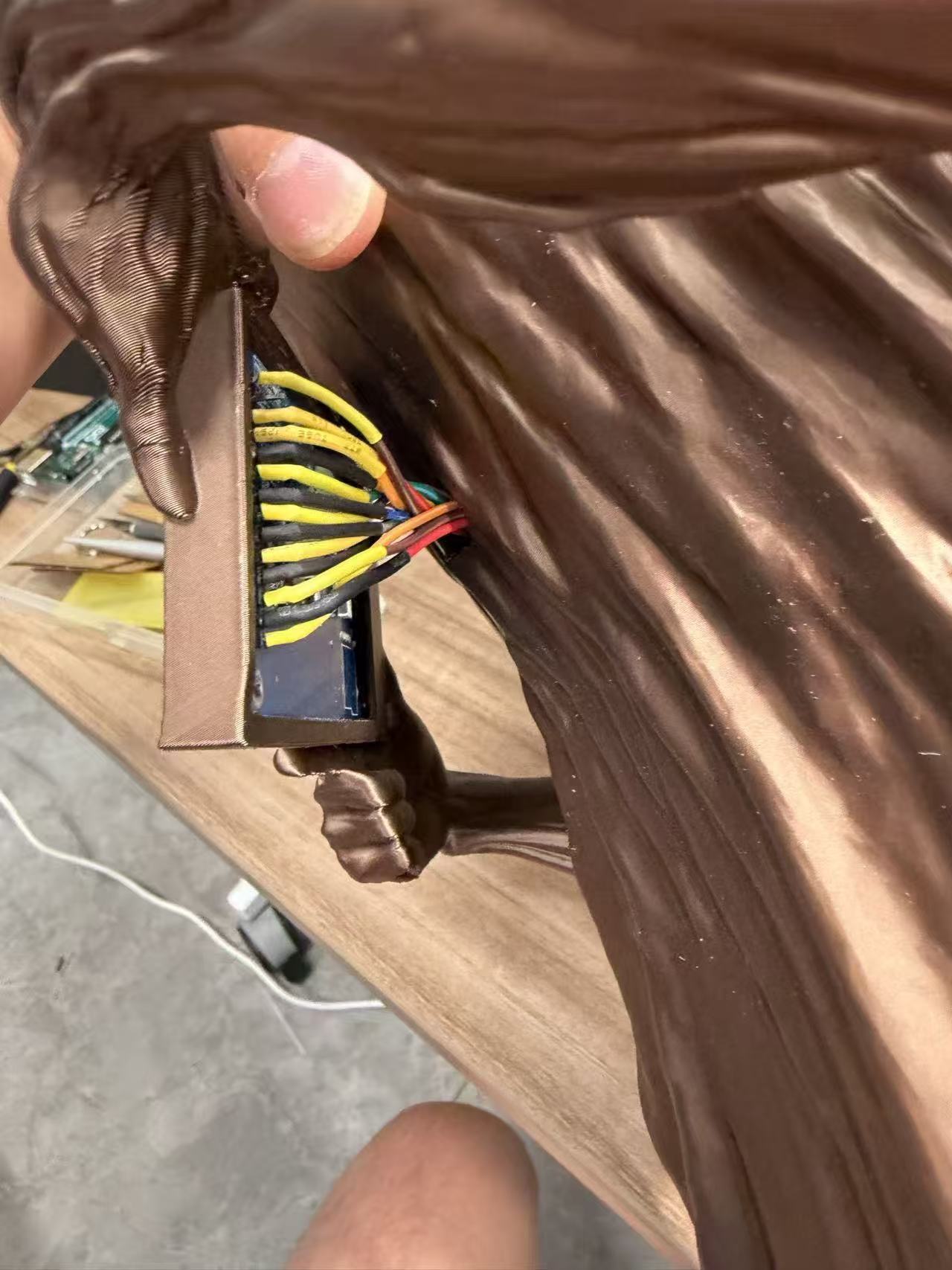
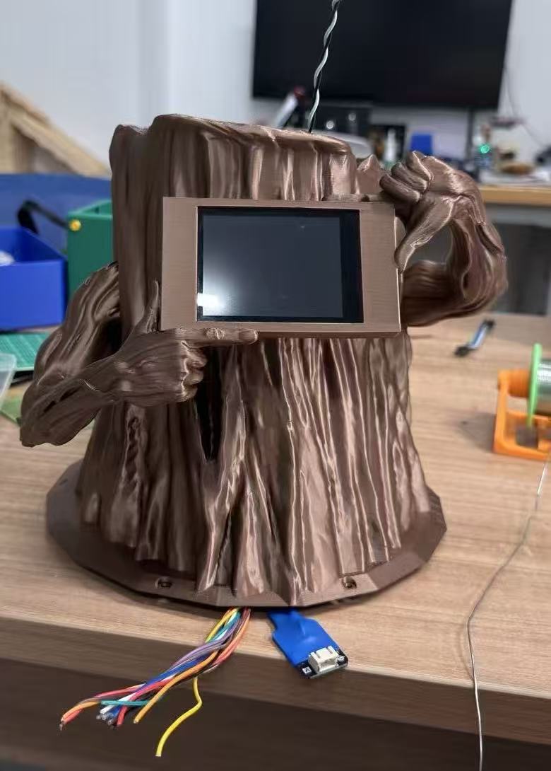
On the integrated machine the ST7789 lives on the front of the pot, while board #2 sits down in the base, so the harness became a mechanical problem as much as an electrical one. I first fed the screen leads into the flowerpot volume from the panel edge, then threaded the same bundle through the pot and out of the bottom opening toward the chassis. Only after the route looked serviceable did I solder the wire ends to the pad groups on the WROOM PCB, matching the photo in §2 and the pin table above.
board_pins.h.
HostLink pin map (hub board #1 ↔ WROOM board #2)
| Signal | XIAO (hub PCB) | WROOM |
|---|---|---|
| I²C SDA | D4 → GPIO9 | GPIO37 |
| I²C SCL | D5 → GPIO8 | GPIO36 |
| 7-bit address | Master writes 0x55 | |
| DHT11 data | D2 → GPIO3 | — (remote on hub) |
| Light ADC | D3 → GPIO4 | — |
Programming — how data reaches the TFT
Step 1 — Hub packs and sends telemetry (I²C master):
// code/week10-i2c-env/xiao/src/main.cpp — pushTelemetry()
Wire.beginTransmission(0x55);
Wire.write((uint8_t*)&pkt, sizeof(pkt));  // magic 0xA5, cmd 0x01, RH, temp×10, light×10
Wire.endTransmission();
Step 2 — WROOM slave parses and bumps redraw version:
// code/week10-i2c-env/wroom/src/env_i2c_slave.cpp — onReceive ISR → ring buffer
// main loop: envI2cDataVersion() changes when a full TelemetryPacked frame arrives
Step 3 — SPI init and pixel draw:
// code/week10-i2c-env/wroom/src/main.cpp — setup()
SPI.begin(Pins::TFT_SPI_SCK, Pins::TFT_SPI_MISO, Pins::TFT_SPI_MOSI, -1);
s_tft.init(240, 320);
s_tft.setSPISpeed(Pins::TFT_SPI_HZ);   // 26 MHz
applyDisplayTransform();               // MADCTL rotation for 320×240 landscape
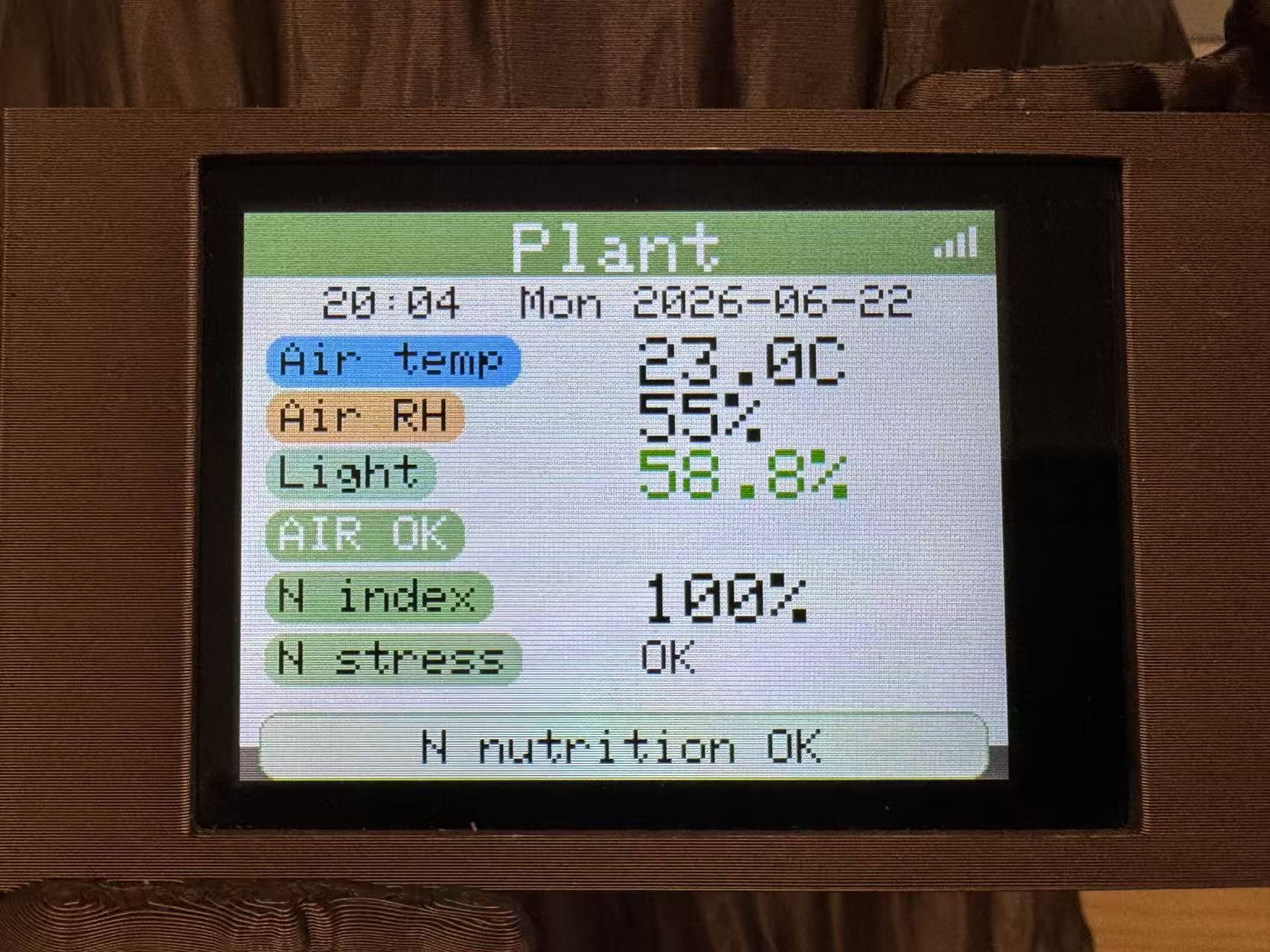
drawPageEnv(envI2cSnapshot());         // Temperature / Humidity / Light + status pill
Each drawPageEnv() call uses Adafruit GFX primitives (fillRect,
printf text) which compile down to ST7789 window set + SPI RGB565 transfers. When I²C delivers a
new frame, loop() compares envI2cDataVersion() and repaints only changed fields.
5. Output device B — separately controlled TFT backlight LEDs (BL)
Working principle
The ST7789 glass is lit by a white LED backlight behind the panel. On my module the BL net is
not part of the SPI protocol — it is a separate power/control line the MCU drives high to turn
the LEDs on. I document it as the second output because it is electrically and programmatically separate from the
SPI pixel bus. In firmware I treat BL as a digital output on GPIO17
(TFT_BL_ACTIVE_HIGH = true in board_pins.h). Without BL enabled the SPI stream can be
correct while the user still sees a dark panel, so I assert BL in setup() before
s_tft.init().
Connection
BL is routed from WROOM GPIO17 through the same harness pad group as the SPI lines (§2 layout
export) to the module’s BL pin. It shares the panel 3.3 V / GND return with the TFT logic
supply on board #2 header U16.
Programming
// code/week10-i2c-env/wroom/src/main.cpp
pinMode(Pins::TFT_BL, OUTPUT);
backlightSet(true);   // digitalWrite(TFT_BL, HIGH)

void backlightSet(bool on) {
  digitalWrite(Pins::TFT_BL, on ? HIGH : LOW);
}
Full UI firmware later adds PWM dimming on the same pin (Week 15); Week 10 uses on/off only.
6. Output device C — I²S speaker through MAX98357 amplifier
Working principle
The front speaker is an audio output. The ESP32‑S3 does not drive the speaker coil directly; it sends a digital I²S stream to a MAX98357 amplifier module. I²S separates audio into a bit clock (BCLK), a left/right word clock (LRCK), and serial audio data (DIN). The amplifier converts that digital PCM stream into the power signal for the speaker. Two extra GPIOs control the amplifier: GAIN fixes the output gain and SD enables or shuts down the amplifier so it is quiet when no sound is playing.
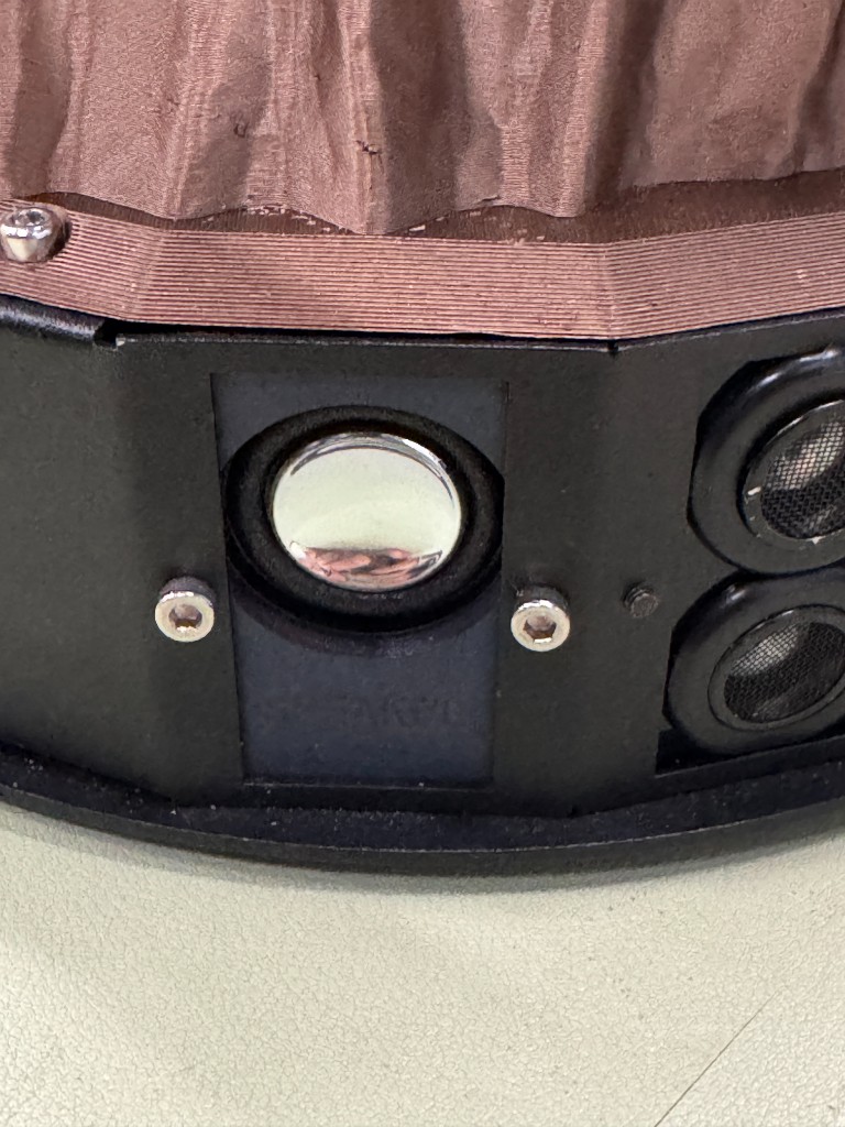
Connection map (WROOM → MAX98357 / speaker)
| Signal | WROOM GPIO | Role in firmware |
|---|---|---|
| I²S LRCK / WS | 42 | audio word-select clock, SPK_I2S_LRCK |
| I²S BCLK | 41 | bit clock, SPK_I2S_BCLK |
| I²S DIN | 40 | PCM data into MAX98357, SPK_I2S_DIN |
| GAIN | 39 | set HIGH during speaker init |
| SD / EN | 38 | amplifier shutdown/enable, driven by enableAmp_() |
| Power / GND | 5V / GND rail | amplifier supply and common ground with WROOM board |
Programming
// code/final-project-upload/wroom-upload/src/board_pins.h
constexpr int SPK_I2S_LRCK = 42;
constexpr int SPK_I2S_BCLK = 41;
constexpr int SPK_I2S_DIN = 40;
constexpr int SPK_GAIN = 39;
constexpr int SPK_SD = 38;
// code/final-project-upload/wroom-upload/src/i2s_speaker.cpp
pins.bck_io_num = Pins::SPK_I2S_BCLK;
pins.ws_io_num = Pins::SPK_I2S_LRCK;
pins.data_out_num = Pins::SPK_I2S_DIN;
pinMode(Pins::SPK_SD, OUTPUT);
pinMode(Pins::SPK_GAIN, OUTPUT);
digitalWrite(Pins::SPK_GAIN, HIGH);
enableAmp_(false);
The test path uses i2sSpeakerPlayTestBeep(), which generates a 440 Hz PCM buffer, enables the
amplifier through SPK_SD, and writes samples with i2s_write(). The same I²S output later
carries streamed voice audio in the final interaction firmware.
7. Output device D — charging dock 1602 LCD (I²C)
Task and board context
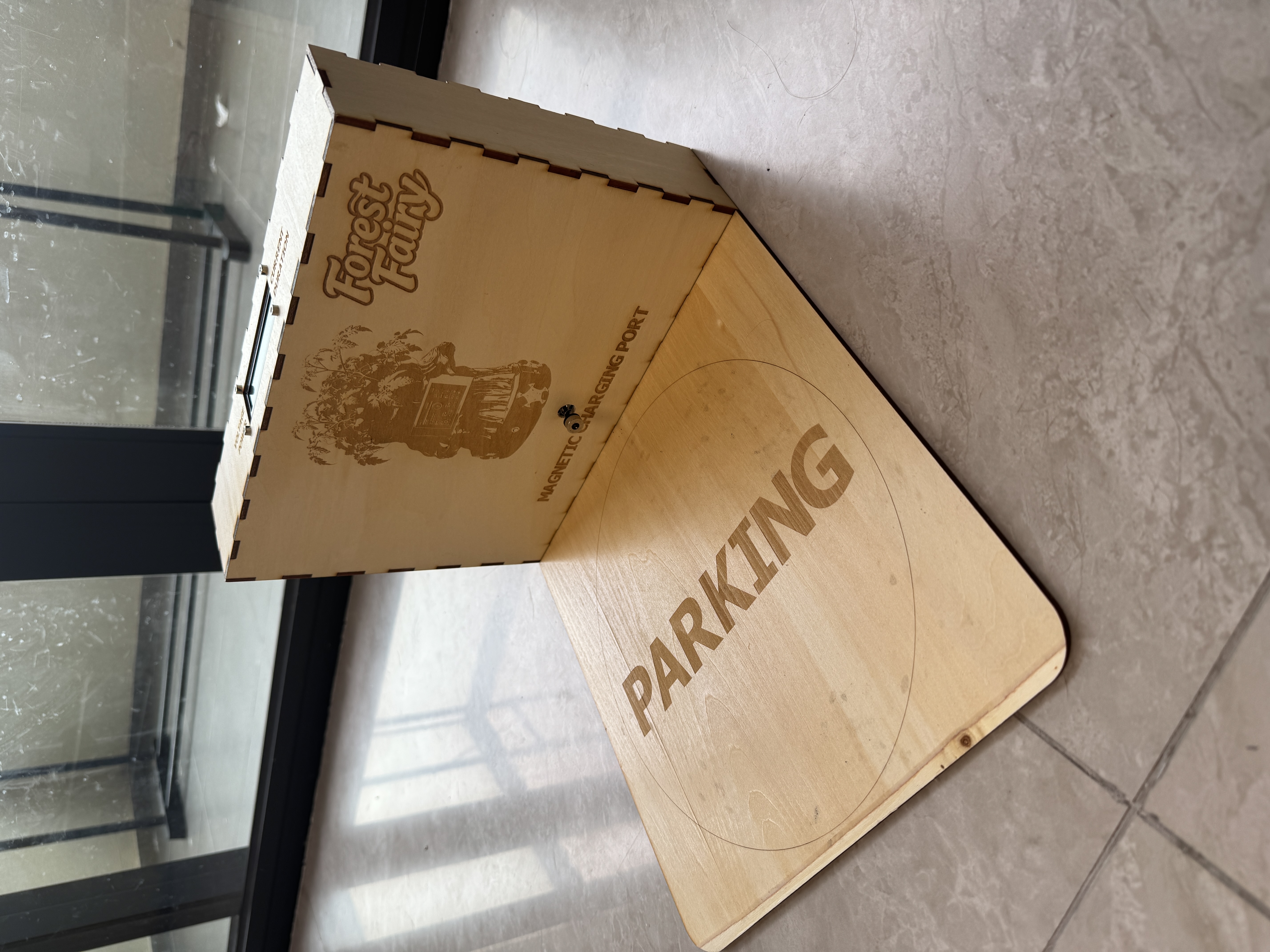
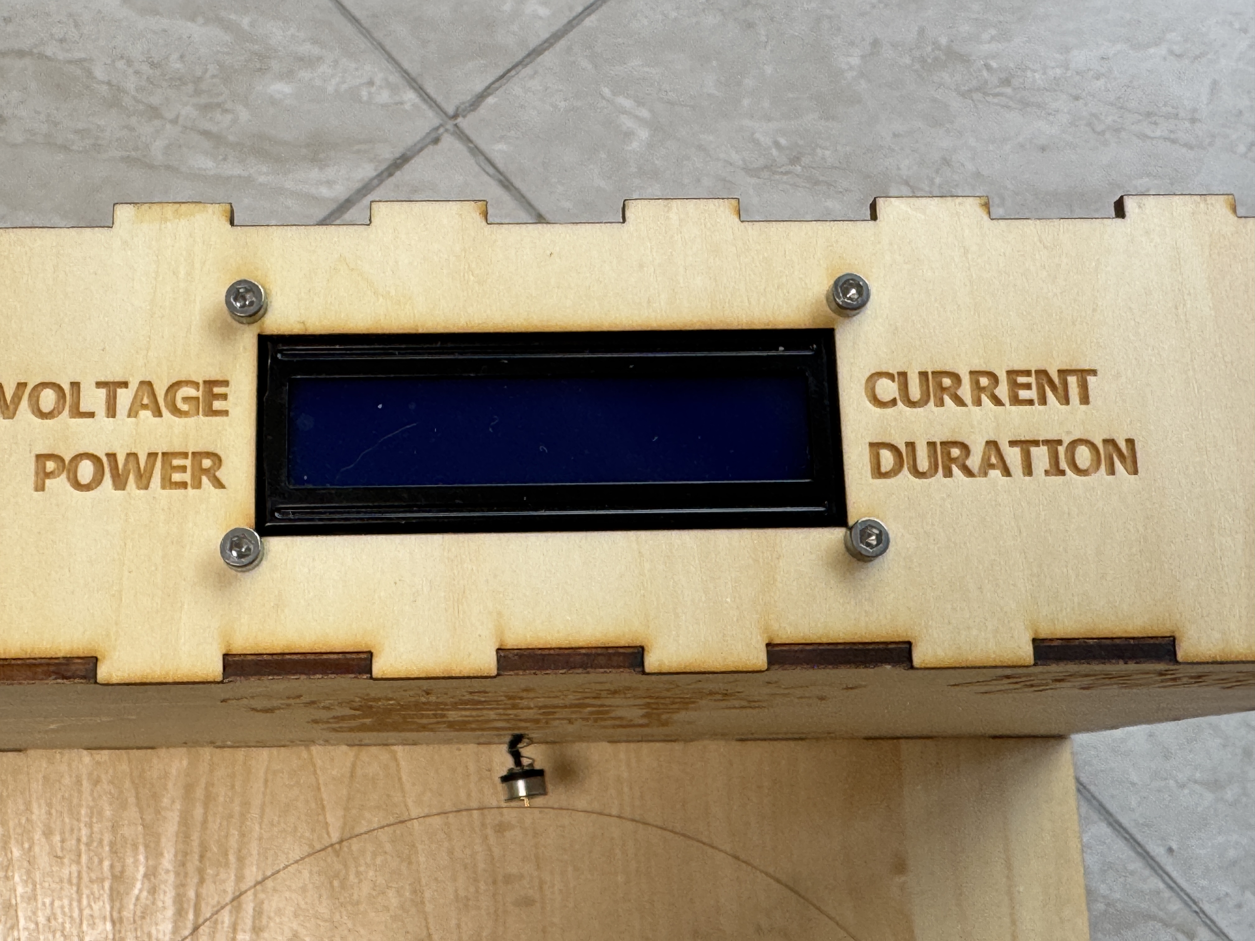
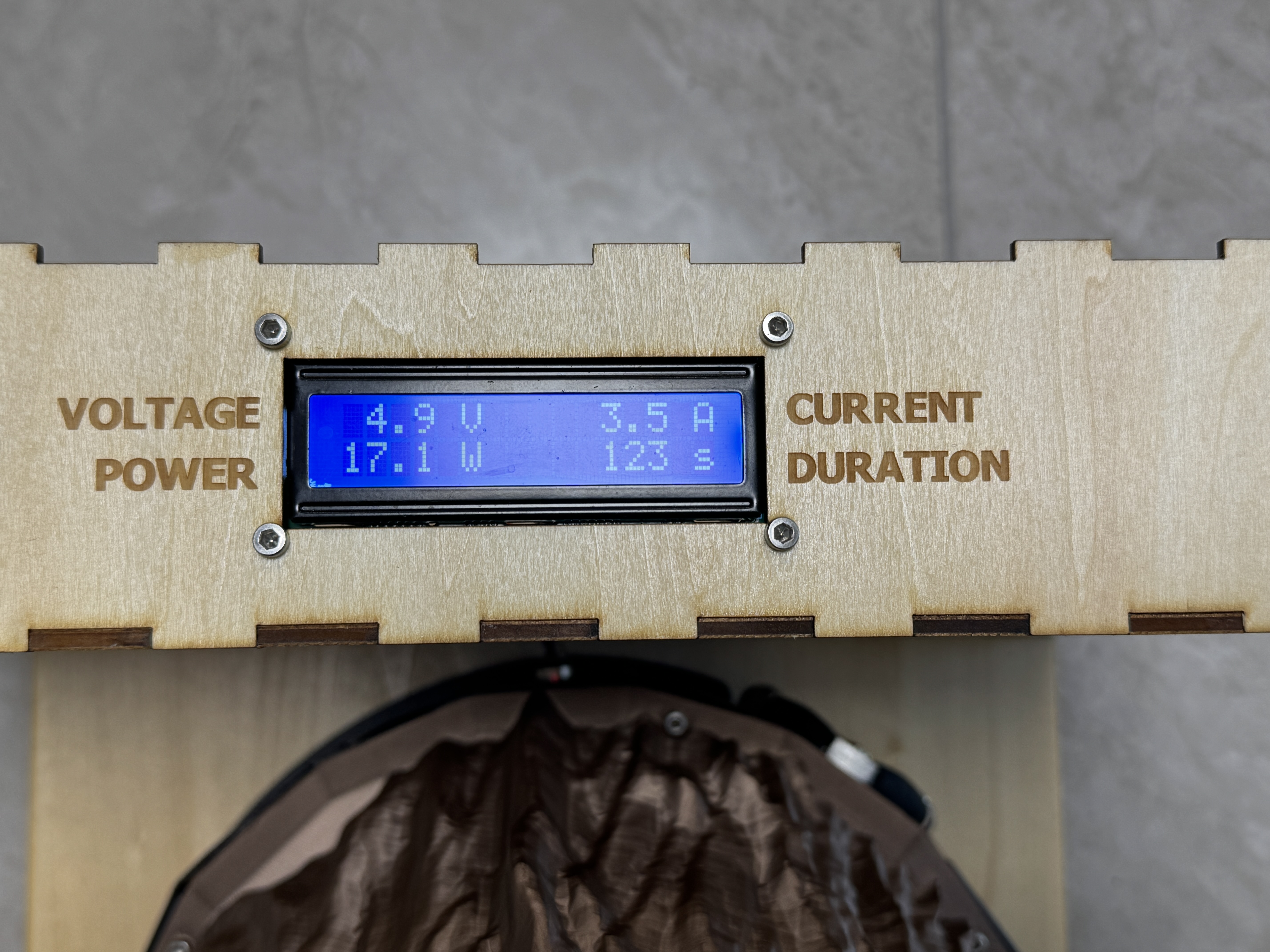
Board #3 is the Forest Fairy charging dock I designed in Week 6 and fabricated in Week 8. In Week 9 I proved the input side — Hall current on A2 and a 1:2 voltage divider on A3 — and logged V/I/P on serial. Output week adds the dock’s main human-facing output: a 16×2 character LCD on I²C that shows the same averaged charge metrics on the enclosure front. The MCU is a Seeed XIAO RP2040 soldered to the dock PCB; the LCD module hangs off the board edge on a short I²C harness.
Working principle
My module is a standard HD44780-compatible 1602 with an on-board I²C backpack
(PCF8574 expander). The RP2040 does not bit-bang parallel RS/E/D4–D7 lines; it talks to the backpack over
I²C at 100 kHz (Arduino Wire default). Each write sets cursor position and
pushes ASCII to the controller; the backpack maps that to the parallel LCD protocol. On boot the firmware scans
addresses 0x20–0x3F, picks the first ACK, then calls LiquidCrystal_I2C::init() and
turns the backlight on with backlight().
Display numbers come from the same ADC path as Week 9: 16-sample averages on A2/A3, Hall zero subtract,
divider ×2 for voltage, then P = V × I. The LCD refreshes every 1 s
(kLcdRefreshMs) with those averages; charge duration (seconds) accumulates only while the
averaged current is ≥ 0.1 A.
LCD pin map (XIAO RP2040 → 1602 I²C backpack)
| Signal | XIAO pin | GPIO | Role in firmware |
|---|---|---|---|
| I²C SDA | D4 | 6 | Wire.setSDA(6) → LCD backpack data |
| I²C SCL | D5 | 7 | Wire.setSCL(7) → LCD backpack clock |
| 7-bit I²C address | Auto-scan 0x20–0x3F; fallback 0x27 | ||
| Power / GND | 3V3 / GND | — | LCD logic and backlight supply (common GND with XIAO and sensors) |
Status LEDs on the same board (D8 FULL, D9 charging) follow the LCD’s 1 s average current — Week 9 documented them as outputs; here the graded output evidence is the LCD paint path. Sensor inputs stay on A2/A3 as in Week 9.
LCD layout (two rows, four fields)
| Row | Left value + unit | Right value + unit | Example |
|---|---|---|---|
| Line 0 | Voltage (V) | Current (A) | 9.8 V 1.2 A |
| Line 1 | Power (W) | Duration (s) | 11.8 W 180 s |
Programming — I²C init and LCD update
Pin constants and I²C setup:
// code/final-project-upload/charging_dock/src/main.cpp
static constexpr uint8_t kPinI2cSda = 6;   // D4 / GPIO6
static constexpr uint8_t kPinI2cScl = 7;   // D5 / GPIO7
static constexpr uint8_t kLcdDefaultAddr = 0x27;

Wire.setSDA(kPinI2cSda);
Wire.setSCL(kPinI2cScl);
Wire.begin();
g_lcdAddr = scanLcdAddress();          // 0x20..0x3F
g_lcdReady = initLcd(g_lcdAddr);       // init + backlight + "Booting..."
Refresh loop — averages ADC, then paints both rows:
// loop(): every kLcdRefreshMs (1000 ms)
const float avgVoltageV = voltageAccumV / lcdSampleCount;
const float avgCurrentA = currentAccumA / lcdSampleCount;
const float avgPowerW = avgVoltageV * avgCurrentA;
updateLcd(avgVoltageV, avgCurrentA, avgPowerW, g_chargeDurationMs);

static void updateLcd(float voltageV, float currentA, float powerW, uint32_t durationMs) {
  snprintf(leftStr, sizeof(leftStr), "%.1f", voltageV);
  snprintf(rightStr, sizeof(rightStr), "%.1f", currentA);
  lcdPrintRowMetric(0, leftStr, 'V', rightStr, 'A');   // row 0: V | A

  formatDurationForLcd(durationMs, rightStr, sizeof(rightStr));
  snprintf(leftStr, sizeof(leftStr), "%.1f", powerW);
  lcdPrintRowMetric(1, leftStr, 'W', rightStr, 's');    // row 1: W | s
}
Full source:
code/final-project-upload/charging_dock/src/main.cpp
·
platformio.ini
· pin and layout notes in
README.md.
PCB layout:
Week 8 charging-dock panel.
8. Plan (execution order)
I started by fabricating and populating board #2, then soldered the ST7789 harness to the
highlighted pad groups and routed that harness from pot to base before closing the mechanical stack. The
next check was HostLink: hub D4/D5 to WROOM GPIO37/36, with pull-ups and a
shared ground, followed by the WROOM week-10 build. I looked for two signs before moving on: the backlight
had to turn on, and serial had to report [HOST_I2C] slave 0x55. After that I used the final
WROOM speaker firmware to verify the MAX98357 wiring on GPIO42/41/40 for I²S and
GPIO39/38 for gain / enable, flashed the XIAO master, and made sure its I²C scan saw
0x55. The final visual check was the live ST7789 UI, first as the simple Environment page and
later as the integrated PLANT INFO page. For board #3, I soldered the charging dock PCB, wired the 1602
LCD to D4/D5, flashed charging_dock, and treated LCD scan plus live
V/I/P/duration as the pass condition.
9. Build diary
HostLink hub (board #1, input side only)
Week 10 does not redesign the hub; it only pushes telemetry over I²C. Sensor bring-up stays on Week 9. Bench wiring is the same D4/D5 link documented in Week 11.
Live TFT output
Downloads — original source files
Week 10 firmware lives in
code/week10-i2c-env/
(HostLink + ST7789 + BL). Speaker output source lives in the final WROOM firmware folder; charging dock LCD
firmware is in charging_dock/. Use
Download if the browser opens a file instead of saving it.
↓ Browse README.md
— wiring, build commands, protocol summary
ST7789 + HostLink path (PlatformIO)
↓ Download xiao/src/main.cpp
— I²C master, DHT11 + light, pushTelemetry()
↓ Download wroom/src/main.cpp
— ST7789 Environment page, SPI init, redraw loop
↓ Download env_i2c_slave.cpp
— I²C slave 0x55 ring buffer
↓ Download board_pins.h
— ST7789 SPI + HostLink pin map
↓ Download i2c_env_link.h
— shared 8-byte TelemetryPacked struct
I²S speaker path (final WROOM firmware)
↓ Download i2s_speaker.cpp
— MAX98357 I²S init, amplifier enable, beep/PCM output
↓ Download i2s_speaker.h
·
↓ Download final board_pins.h
— speaker API and WROOM GPIO map
Charging dock 1602 LCD (PlatformIO — board #3)
↓ Download charging_dock/src/main.cpp
— I²C LCD on D4/D5, ADC → V/I/P/duration display
↓ Download platformio.ini
·
↓ Browse README.md
— pin map and LCD layout
PCB design — board #2 WROOM display (Output week)
↓ Download wroom-pcb.eprj2
— 嘉立创 EasyEDA project (ESP32‑WROOM + screen pads + power)
PCB design — board #3 charging dock (Week 6/8)
↓ Download charging-station.eprj2
— 嘉立创 EasyEDA project (double-layer dock: XIAO RP2040 + current sense + LCD header)
·
Week 8 fab + soldering photos
PCB design — board #1 hub (reference, Week 6/8 — not Output week assessed board)
↓ Download v1.kicad_sch
·
↓ Download v1.kicad_pcb
— XIAO + Pico hub; FPC on this panel only
Problems I hit
Most failures were wiring or firmware-order problems, not mysterious display bugs. When the scan did not show
0x55, the cause was usually that the WROOM was not flashed yet, ground was missing, or the pull-ups
were too weak. When the TFT showed WAIT S3 0x55, the WROOM slave was alive but the XIAO master was
not sending, or SDA and SCL were swapped. A dark panel with good serial meant SPI was probably fine but
TFT_BL was not driven, so I checked the BL wire and backlightSet(true). For the speaker,
the useful checks were MAX98357 SD high during playback, common ground present, and I²S
LRCK/BCLK/DIN not swapped. On the dock, a blank LCD at boot was usually an I²C address or SDA/SCL problem, so I
watched serial for [I2C] found device at 0x.. and confirmed D4/D5 mapped to
GPIO6/7. If the TFT showed DHT ERR even when hub serial looked good, the missing piece was the
kFlagDhtOk bit in the telemetry flags.
10. Conclusion
I used Cursor to code the HostLink + ST7789 teaching firmware in
code/week10-i2c-env/ and to refactor the speaker and charging-dock
output paths under final-project-upload/. I still matched every
pin name to board_pins.h, flashed each board, and fixed I²C scan and backlight issues from serial and
on-screen symptoms before calling a build working.
Output week covers two boards I designed. On board #2 (WROOM display PCB), I programmed ST7789 pixels over SPI, backlight on GPIO17, and I²S audio through MAX98357, with telemetry fed by HostLink from hub board #1. On board #3 (charging dock) the 1602 I²C LCD on D4/D5 is the main output — it shows the charge metrics I first validated on serial in Week 9. The pot-to-base TFT harness, EasyEDA layout, speaker pin map, and dock LCD placement are custom provisions, not off-the-shelf dev kits. The same stack carries into Week 11, Week 15, and Week 16 packaging.
Design files:
wroom-pcb.eprj2 (board #2) ·
charging dock (board #3) ·
Week 6 hub (board #1) ·
Week 8 production.
Group reflection:
power measurement below.
Group assignment (Chaihuo Makerspace)
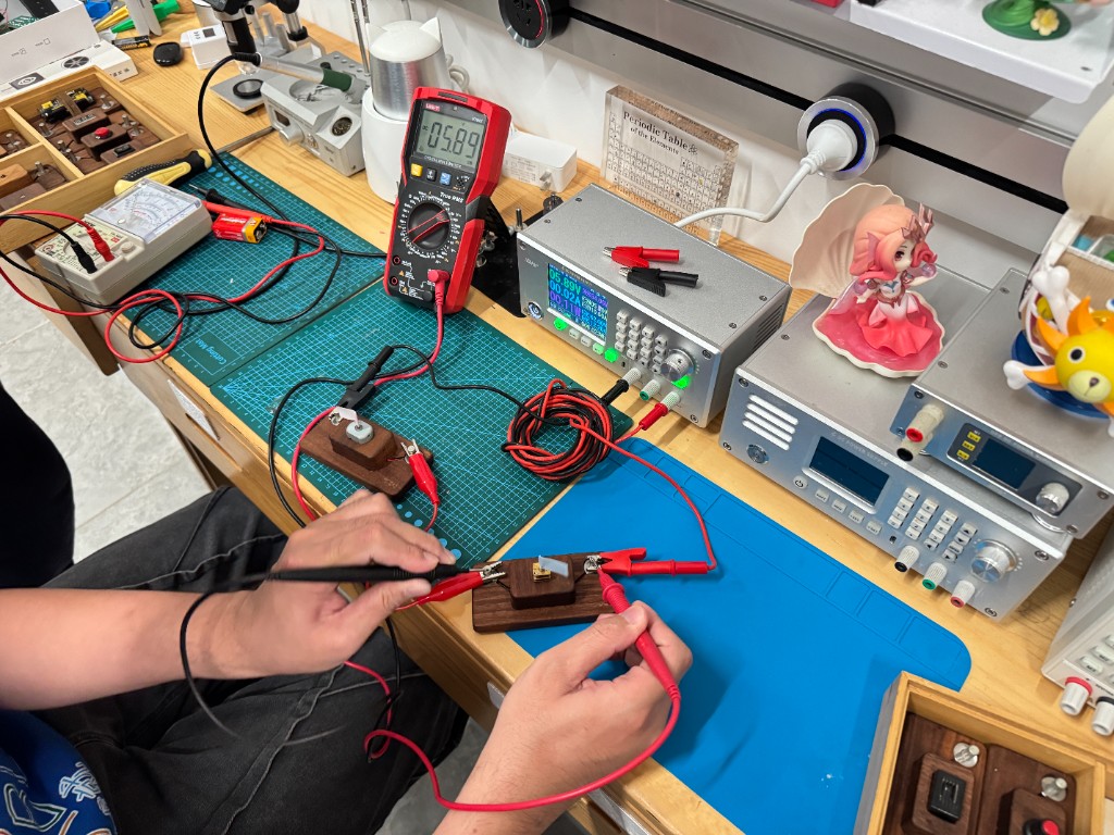
The Fab brief for output week asked us to measure power on an output device with bench gear and write down what we saw. Our Guangzhou cohort ran that on a simple load fixture before anyone plugged in a TFT or motor on their own board. Individual work stayed on custom boards (above); this section is the shared bench method.
Bench setup
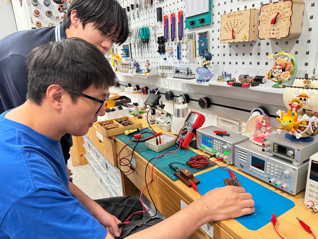
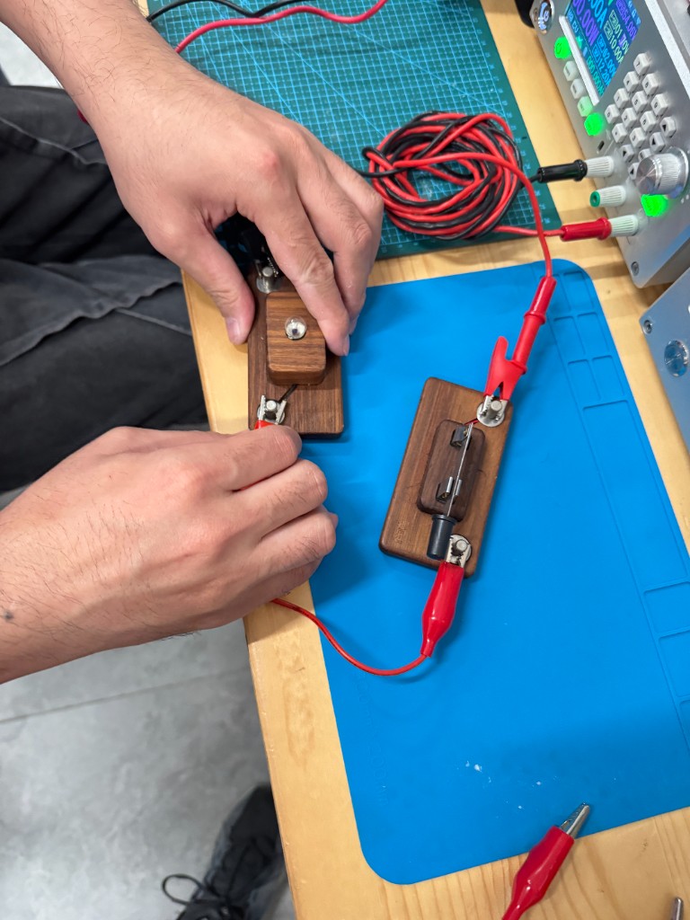
We used a CV-mode DC supply, a handheld DMM, a small output load fixture, and a pile of alligator clips. Nothing exotic, but we agreed on one rule up front: let readings settle before writing numbers down, and note whether the supply or the meter was the source of truth for current.
How we calculated power
We used the usual relation:
P (W) = V (V) × I (A)When we had a known resistor in the loop, we also checked current with Ohm's law from the voltage across it:
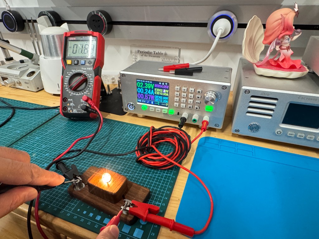
I = V / RLoad ON
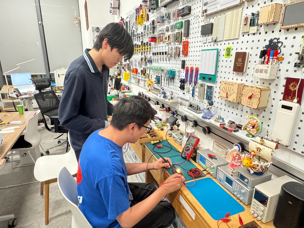
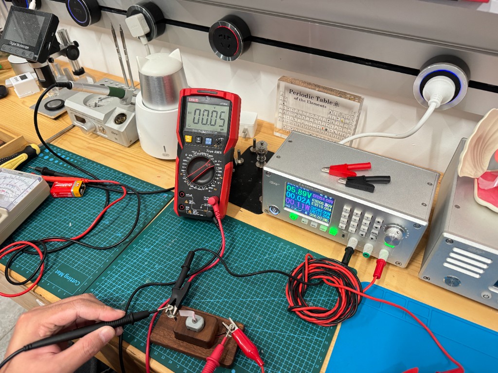
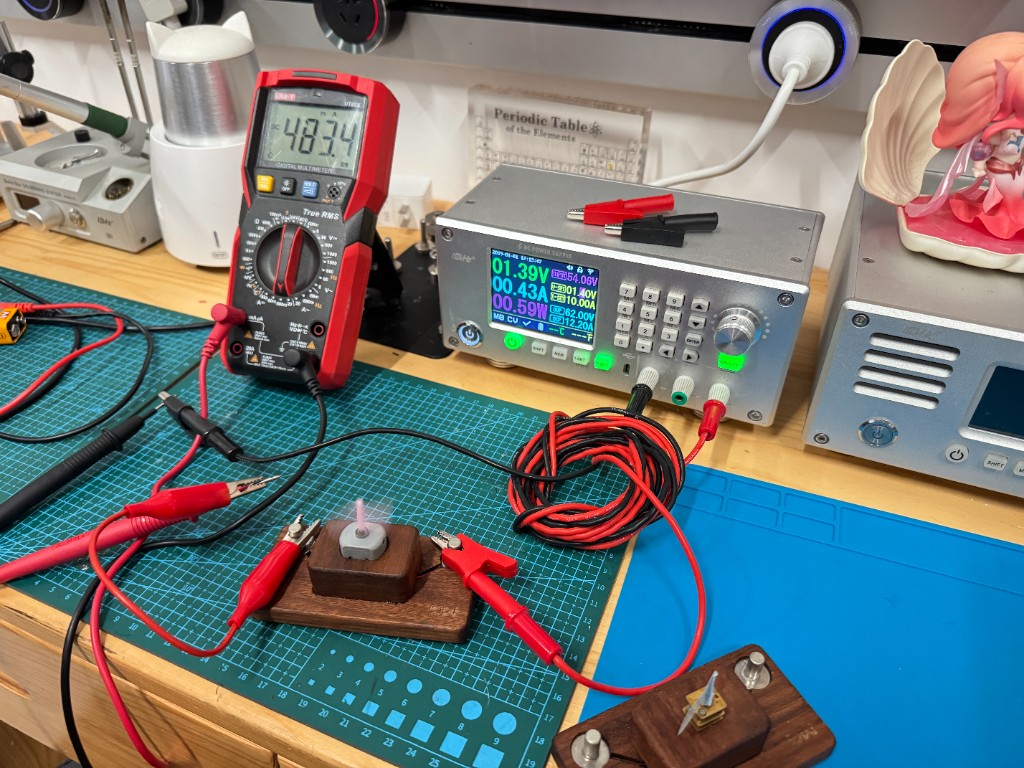
With the fixture connected and the load energized, we waited until the supply display and DMM agreed within a few milliamps, then wrote down V and I. Photos below are the team at the bench and two meter snapshots from the same run.
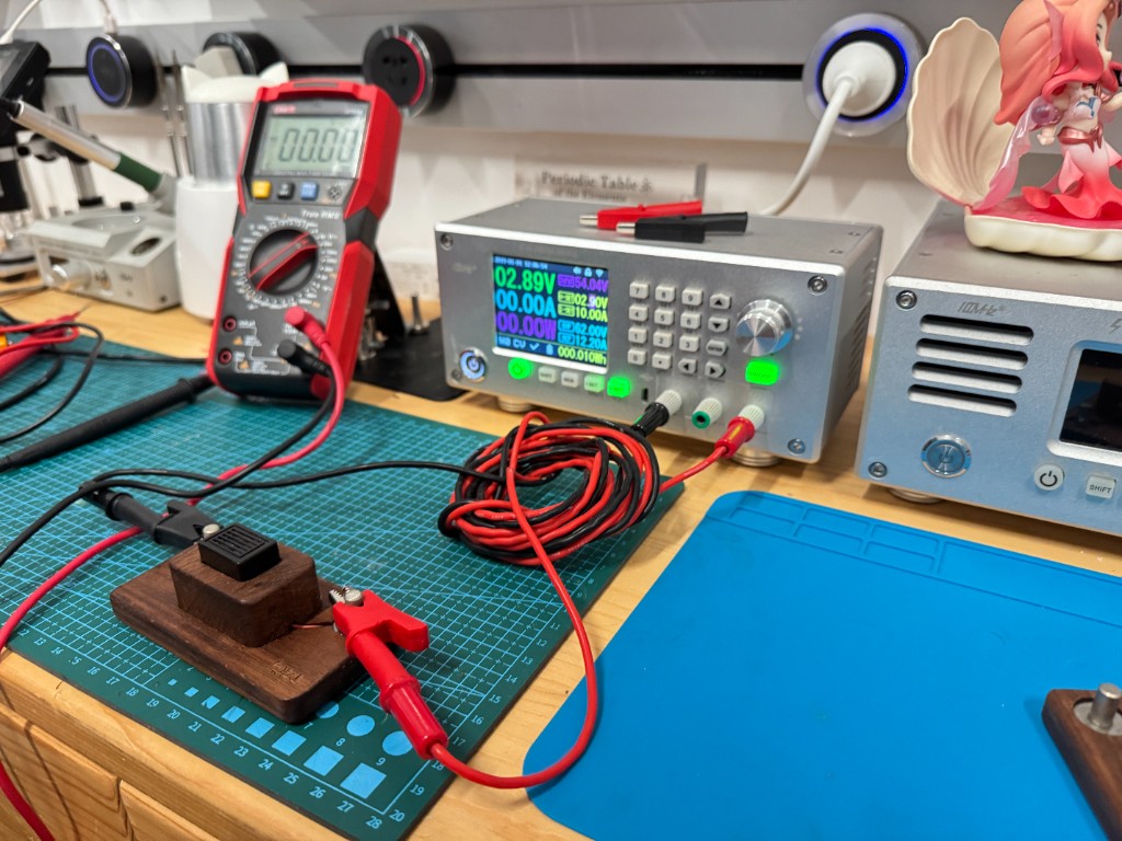
Open-circuit baseline
We opened the loop on purpose to confirm the supply reported near-zero current with nothing drawing. That caught one mis-clipped lead early in the session before we trusted loaded numbers.
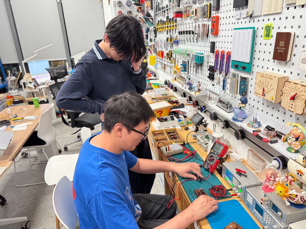
Repeated runs
We cycled the load a few times and watched current move with operating state. Readings were repeatable enough that I felt comfortable using the same clip layout when I later measure backlight draw on my WROOM board.
What we wrote down
| Condition | What we saw | Takeaway |
|---|---|---|
| Load ON | Current and P = V×I above the open-circuit floor | The fixture actually draws power when energized |
| Open circuit | Current near zero on supply and meter | Baseline wiring looked sane |
| Repeated toggles | Readings tracked load state each time | Same clip layout gives comparable numbers run to run |
The group exercise did what we needed: a shared way to quote milliamps and watts before blaming firmware. I reused the supply-and-meter habit when checking TFT backlight load on my own output board.