Week 8: Electronics production
Electronics production week. On my individual page I ran the in-house mill once (Gerber → Mods → CNC), kept that copper as a mistake record, and moved the working build to a JLCPCB rev 2 panel. The working board below is that JLC assembly: XIAO ESP32-S3, FPC, and a NanoStat/Pico sidecar with removable fly wires. UART proof is in the serial capture further down. Chaihuo operating notes are under Group assignment.
Individual assignment: mill, stuff, and fab-order my dev board
Fab Academy Electronics Production asks for a microcontroller development board I designed, with evidence for toolpaths, milling (or outsourcing), stuffing, soldering, debugging, and a working program. I laid out the carrier in Week 6. This week I had to show I can run the lab workflow, order a fab spin when milling is not enough, and bring the board up with firmware that actually runs.
1. Task
My carrier hosts a Seeed XIAO ESP32-S3, an FPC toward a display, and (from rev 2 onward) a side panel for a NanoStat / ESP32 Pico stack. I care about this board because it is the hub my final project keeps reusing: room sensors on the XIAO, plant stats from the Pico over UART, display traffic out over I²C. Week 8 is where that hub stops being a KiCad file and becomes something I can solder and flash.
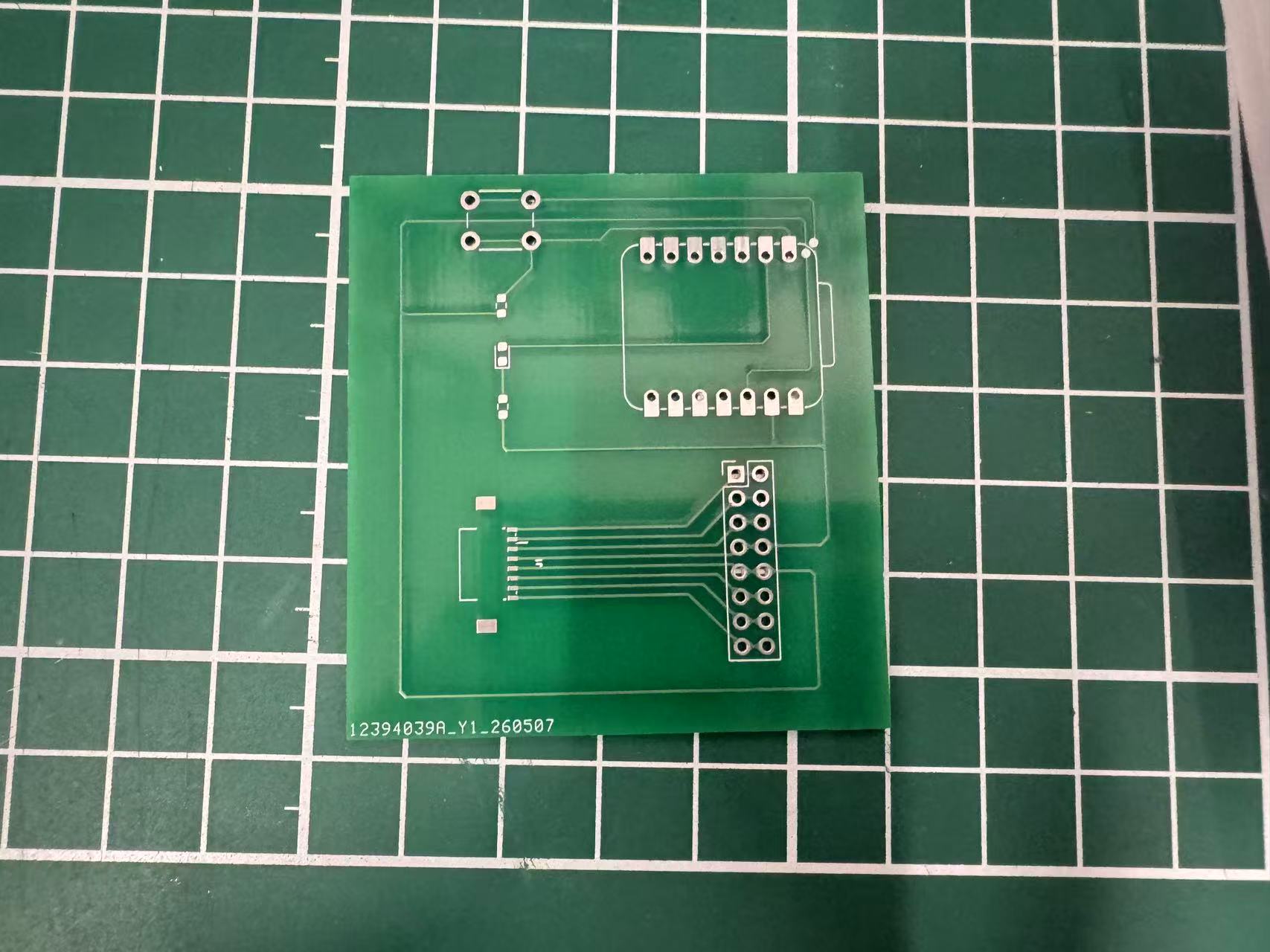
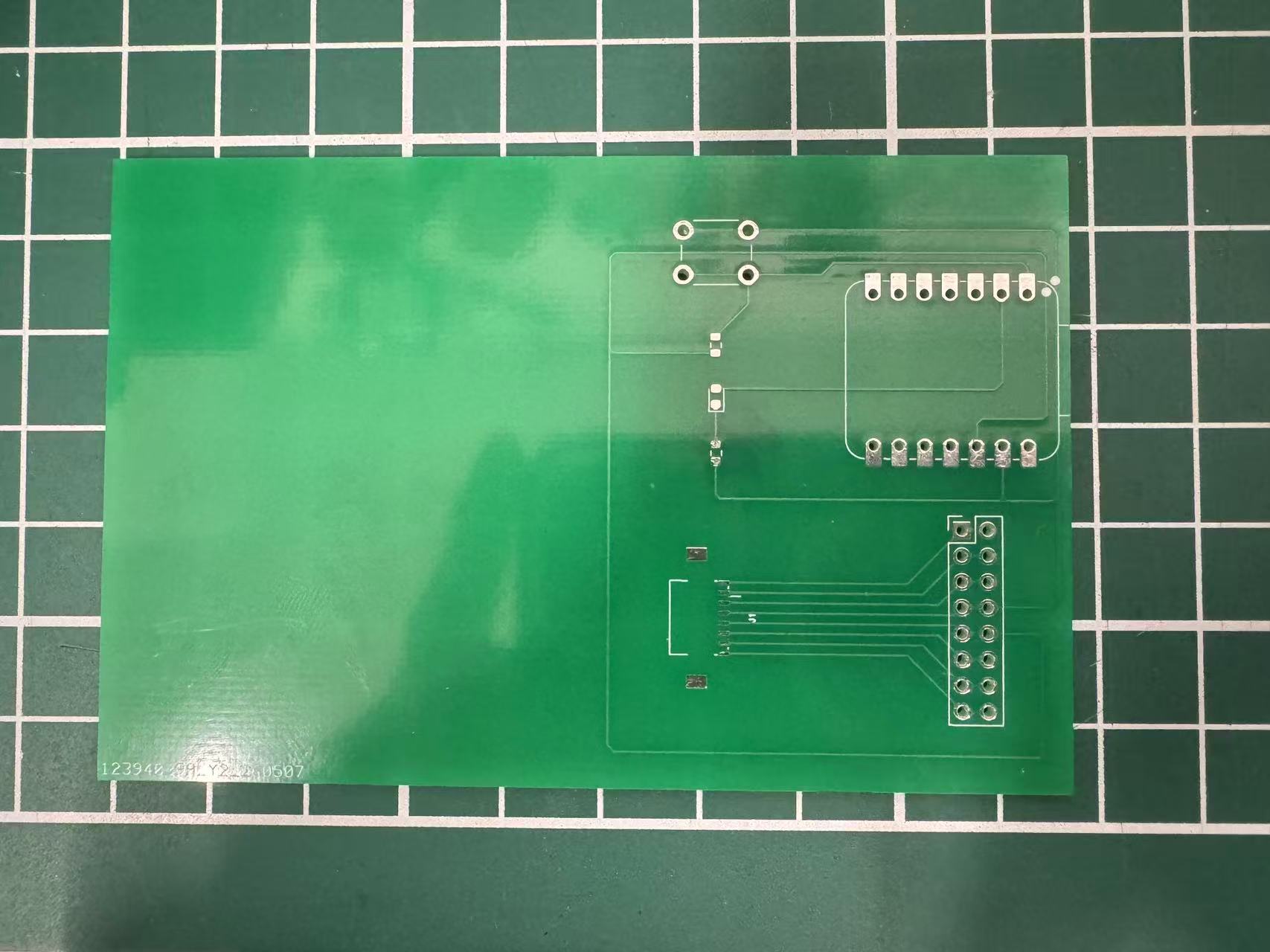
I planned two production paths on one page. First, a CNC-milled copper prototype to prove the Week 6 layout is routable on the Chaihuo mill. Second, a JLCPCB panel for the board I could reliably stuff and program. The same week I also sent two more EasyEDA layouts to JLC: a WROOM display carrier (board #2) and a charging-dock PCB (board #3). I did not re-mill the hub after the first run. The milled copy stayed as process evidence (toolpath, deburr, continuity). The board I assess for Week 8 is hub rev 2: solder mask and wider SMT pads made the XIAO castellations and Pico header much easier than bare milled copper.
| Nueval checklist item | Where on this page |
|---|---|
| Linked group assignment | Chaihuo mill operating notes |
| Documented toolpath generation | Gerber → PNG → Mods → G-code |
| Documented plan and both production paths | Section 3 plan (mill + JLC tracks) |
| Documented mill / stuff / solder / debug | Mill run, Milled continuity, WROOM PCB, Charging-dock PCB, Dock soldering, Hub programming |
| Board functional + source uploaded |
UART serial proof
(week08-xiao-bringup.ino,
hub firmware linked in section 4)
|
| Hero shot | Hub UART serial proof (below) |
2. Learning
I re-read the academy production notes and our group mill checklist (below). For in-house work the chain is Gerber → PNG → Mods → edited G-code → mill. Isolation depth, tool diameter, and Z touch-off still decide whether traces stay connected. Milled copper is not the same as a fab board: no mask, no plating, and burrs can bridge nets until you deburr.
I also walked through the JLC client upload flow even though I already knew I would order panels. The nueval FAQ says you do not have to push the final order button, but you do have to document the path to it. That matched what I needed anyway: plated holes, solder mask, and enough pad margin to hand-solder the XIAO. When the milled copy’s castellated pads felt too tight, ordering rev 2 was the obvious next step instead of fighting bare copper.
3. Plan
I split the week into two tracks that share one write-up. Track A (lab mill):
export Gerbers from Week 6, run Gerber2PNG and Mods, post-process G-code for the Chaihuo
controller, mill once, deburr with P800, attempt a partial solder, then continuity-check before
USB. Track B (JLC rev 2 hub + two satellite boards): upload Gerbers through the desktop
client for the hub, WROOM carrier, and charging-dock PCB; solder XIAO + FPC + passives on hub
rev 2; mount the Pico sidecar with removable fly wires; meter-check; upload
week08-xiao-bringup.ino and then the hub
+ Pico bridge firmware until Serial Monitor shows [PICO RX] STAT,… lines. I kept
Track A photos even after Track B became the functional board.
4. Operation
In-house CNC: toolpath, mill, deburr, solder, continuity
From KiCad Gerber to machine-ready G-code
The assignment needs the toolpath workflow spelled out, not just a finished board. My carrier layout lives in Week 6; this week I exported the same Gerber stack, ran it through the lab’s PNG → Mods → G-code chain, post-processed the files for our Chaihuo controller, and only then clamped stock and hit cycle start. The archived upload is week08-carrier-gerbers.zip.
Step 0 — Export Gerber from KiCad
In KiCad I used File → Fabrication Outputs → Gerbers (plus the drill file if the job needs it). Our mill flow only needs the top copper and board outline layers in the zip; I kept layer names aligned with what Gerber2PNG expects so I would not have to rename files by hand.
Step 1 — Gerber → PNG (traces.png, outline.png)
I opened
gerber2png.fablabkerala.in, uploaded the zip, left Copper mode: Top, and used
Quick setup → Generate All. The preview matched my Week 6 board
(XIAO footprint, FPC J1, pour on the right). I downloaded the generated
traces and outline PNGs at 1000 DPI — those two
files are the only inputs Mods needs on our side.
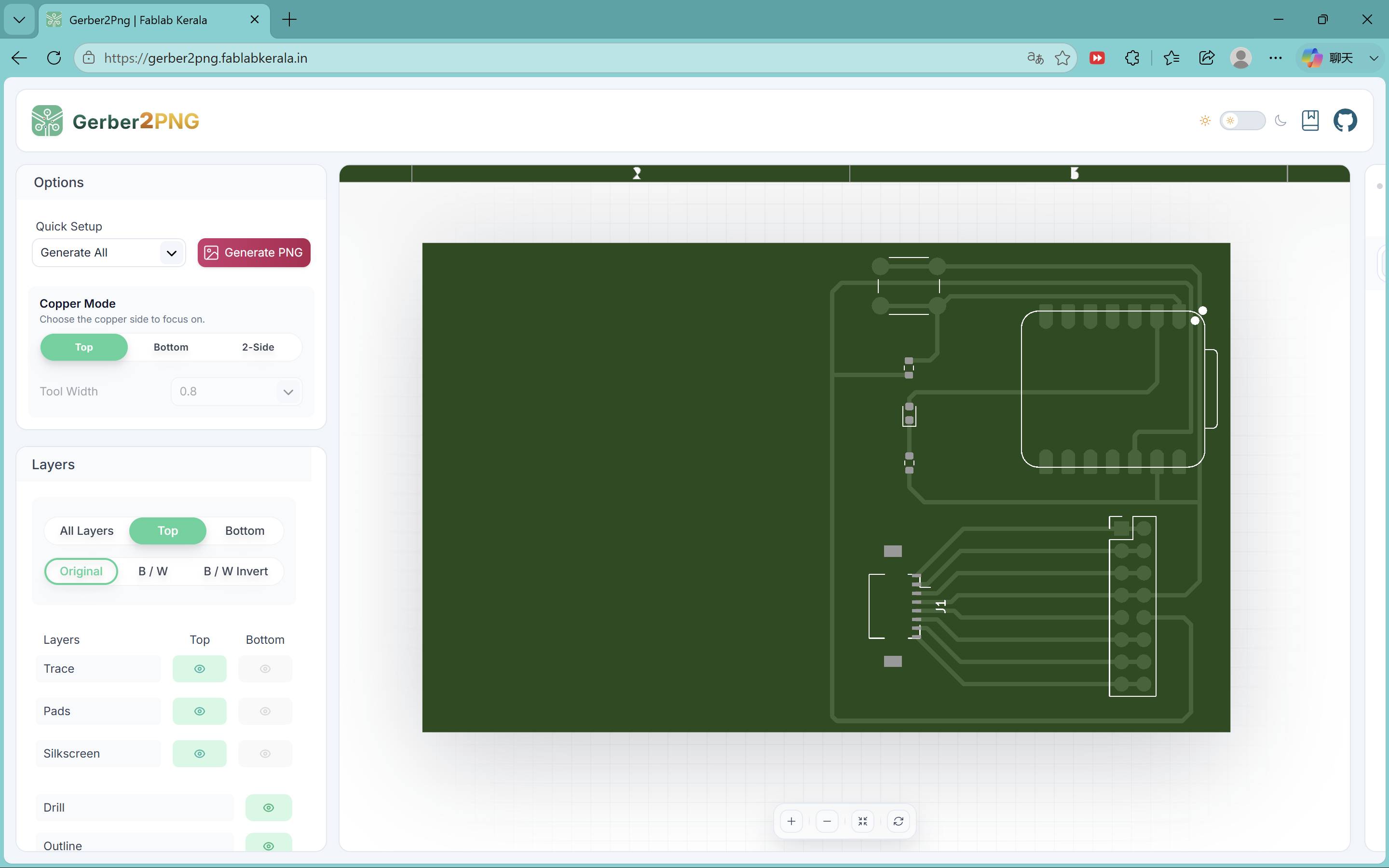
traces.png and outline.png.
Step 2 — Load PNGs in Mods CE
In the browser I opened the Fab mill program:
Mods CE — mill 2D PCB. The left read png node is where each PNG lands. I ran the workflow
twice in total — once with traces.png, once with
outline.png — and kept the other Mods defaults unless noted below.
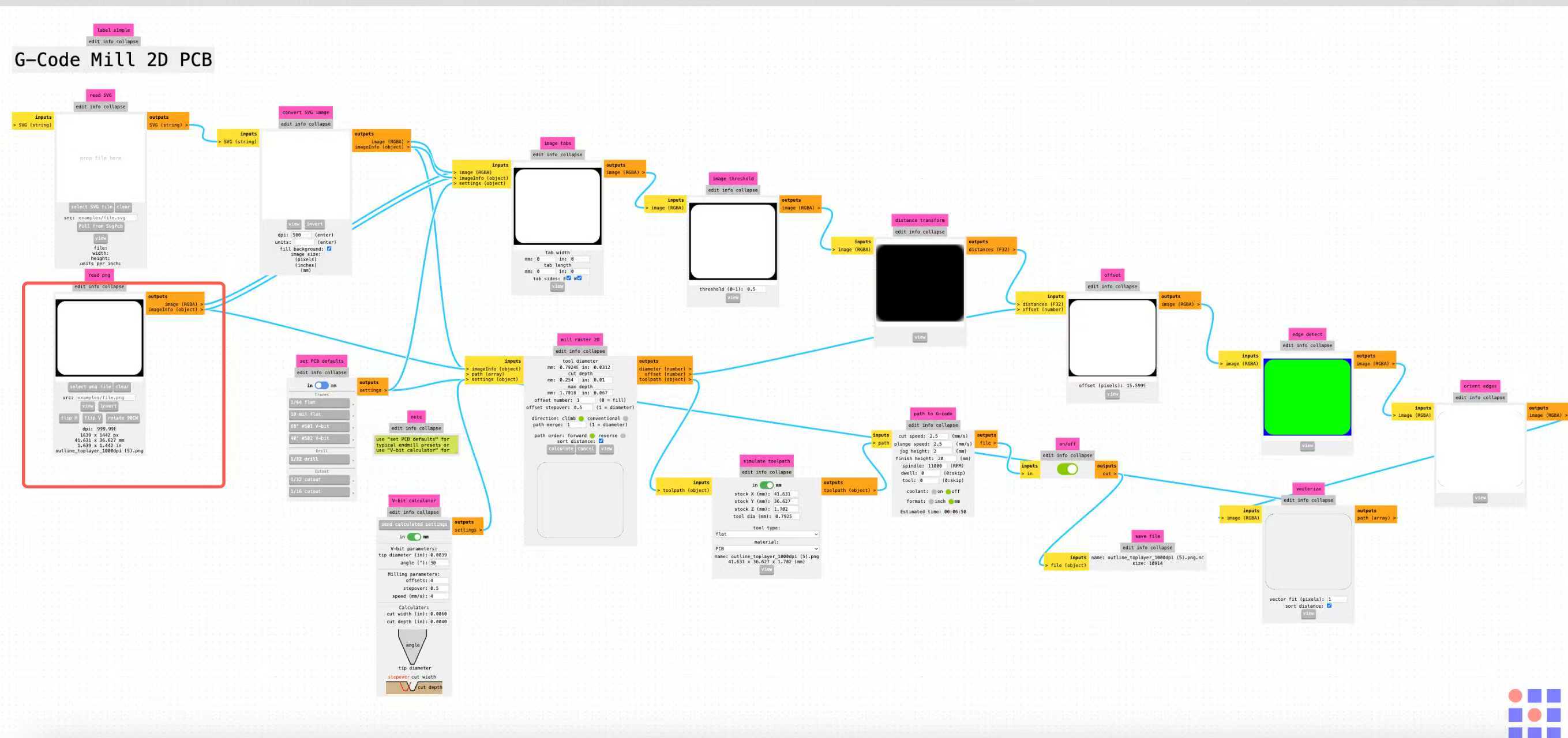
outline.png in the read png node (red
box). The same node accepts traces.png for the isolation pass.
Design rules vs. tool choice (Chaihuo + my layout)
My Week 6 carrier targets roughly 6/6–8/8 mil trace and gap (≈0.15–0.20 mm) around castellated XIAO pads and an FPC footprint — dense enough that the tool preset has to match the layout, not whatever Mods highlights first. Fab isolation milling convention (and our group notes) is a 1/64″ (~0.40 mm) flat end mill with several contour offsets, not a 1/32″ bit and not a large V-bit pretending to be a trace cutter. Outline cutting uses a separate 1/32″ (~0.79 mm) end mill through the 1.6 mm FR1.
| Pass | Physical tool (lab) | Mods preset | Key parameters | Why for this board |
|---|---|---|---|---|
| Traces | 1/64″ flat end mill (~0.396 mm) | 1/64 flat (Traces group) | cut depth 0.10 mm; offset 4; stepover 0.5; cut/plunge 2.5 mm/s; spindle 11 000 RPM | Bit width matches minimum gap; four offsets clear copper between 6/6 nets without gouging pads. |
| Outline | 1/32″ end mill (~0.794 mm) | 1/32 drill (Outline group) | cut depth 0.25 mm per pass until through stock; offset 1; same feeds/spindle as traces | Wider bit only for board profile; keeps tab/slot geometry outside the copper pattern. |
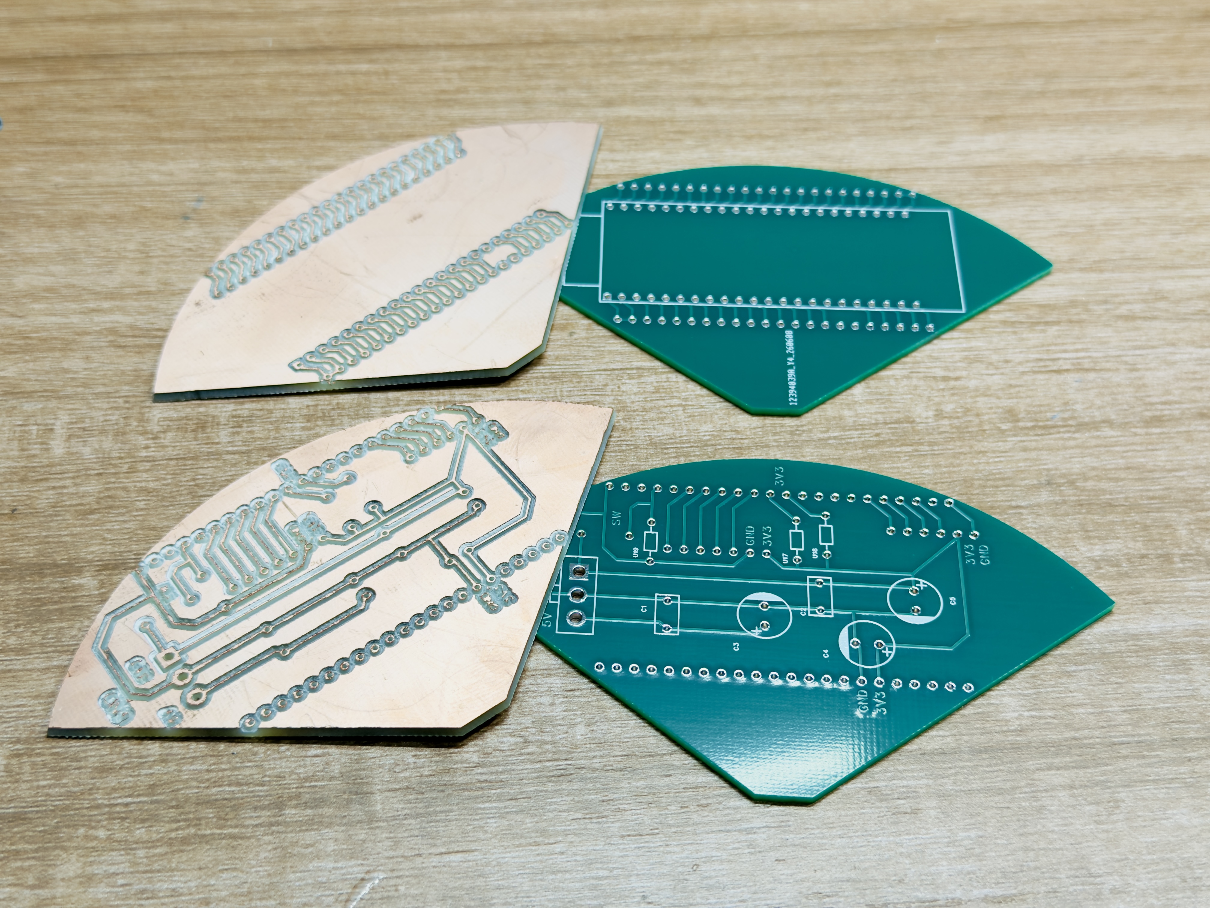
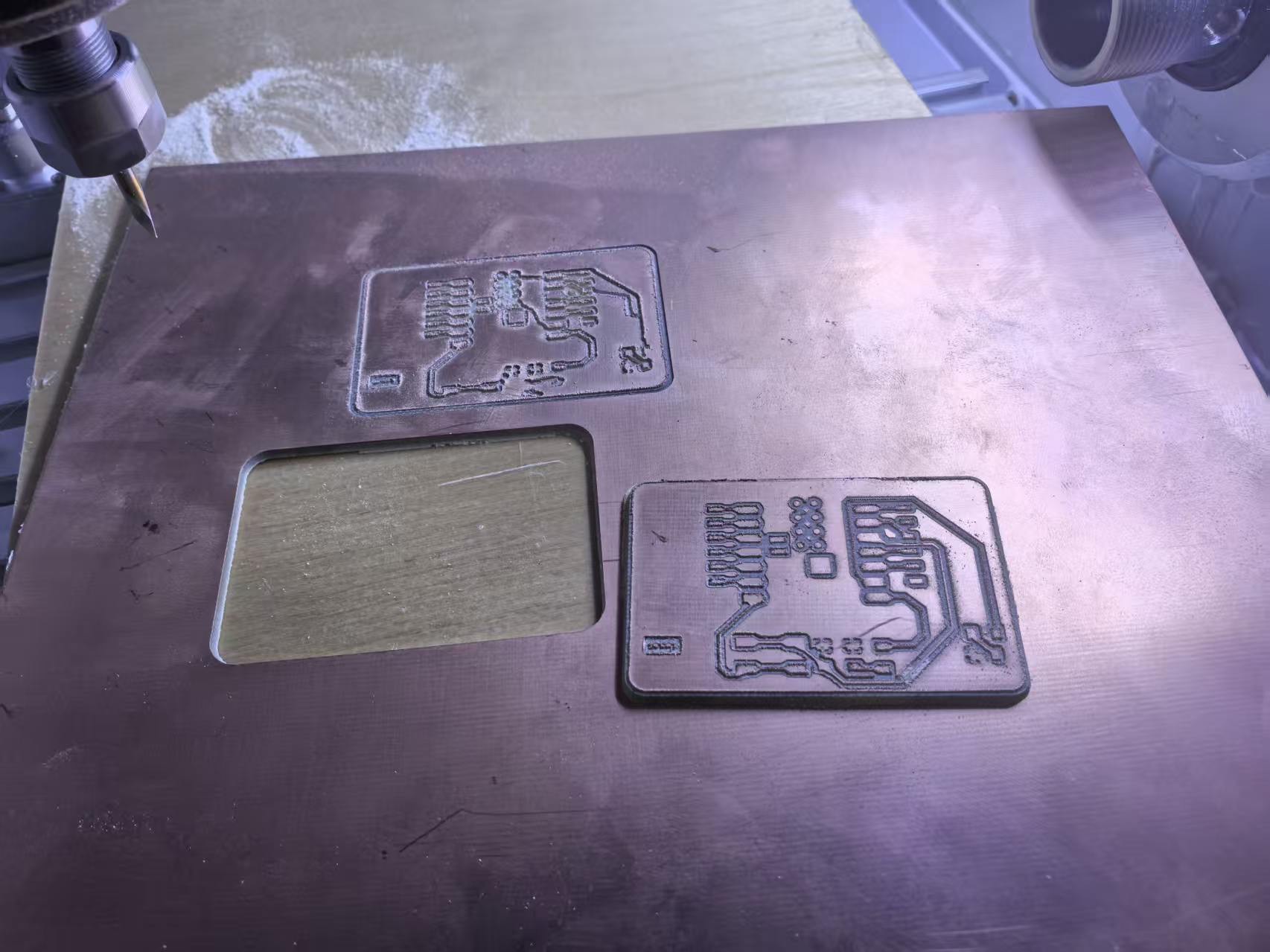
What went wrong on the first milled run: I picked the wrong Mods preset once (40° V-bit, ~0.79 mm effective width, offset 1. Screenshot below). That is not the usual Fab trace recipe for a 6/6 layout. On the machine it smeared copper and left burrs (see mill photos). I deburred with P800, checked continuity, and kept that board as evidence of the mistake. I did not re-mill a second copper panel. Instead I documented the correct 1/64 flat / offset 4 Mods block (next figure) for next time, and moved hand assembly to the JLC board where pads and mask are easier to solder.
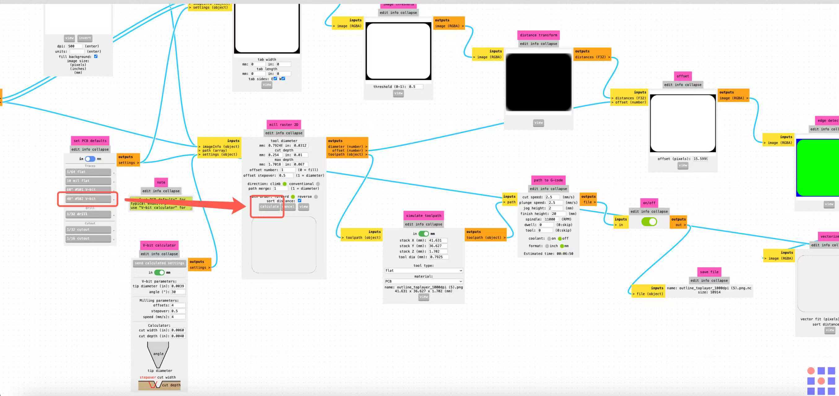
Step 3 — Calculate toolpaths and enable download
3.a Traces (isolation): load traces.png, choose
set PCB defaults → Traces → 1/64 flat, confirm
mill raster 2D reads about 0.396 mm tool diameter,
0.102 mm cut depth, offset 4, then click
calculate and inspect view toolpath before saving.
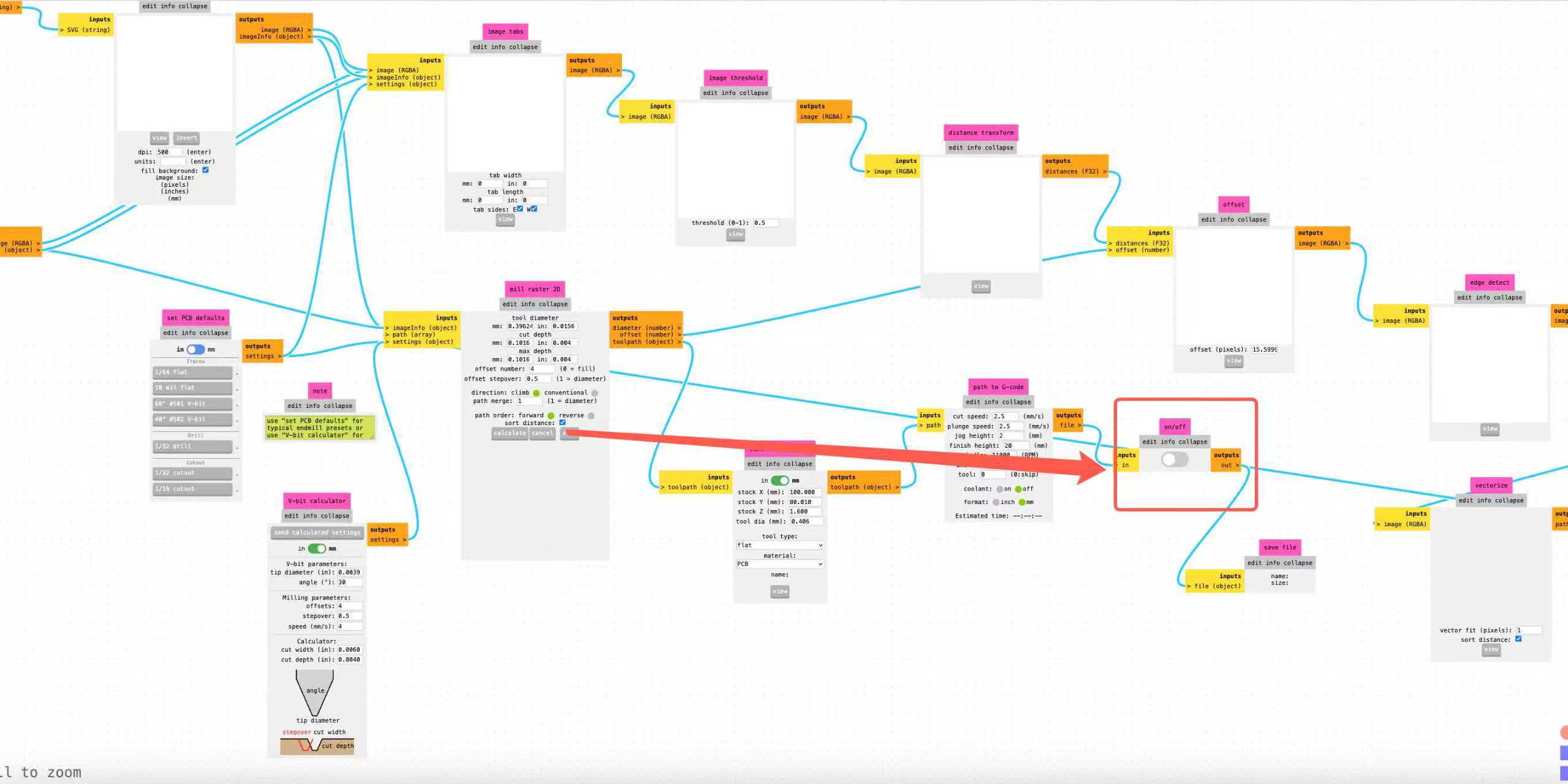
*.nc.
3.b Outline (board cut-out): swap to outline.png, choose
set PCB defaults → drill → 1/32 drill, verify max depth cuts through
1.6 mm FR1, click calculate.
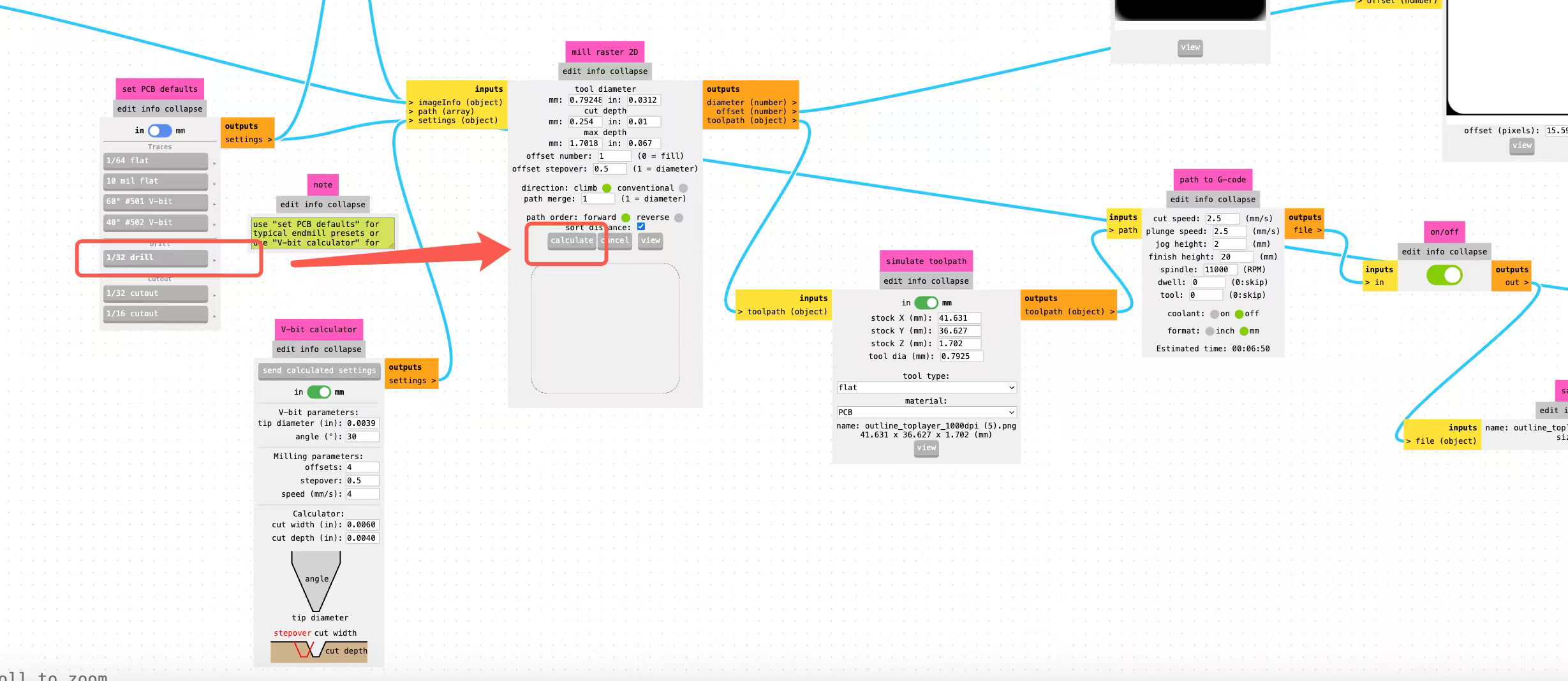
3.c File output: for both passes, flip the on/off node
ahead of save file to on before you click
calculate (shown in the trace screenshot above). Otherwise Mods renders
the path but the browser never downloads the .nc file.
Step 4 — Post-process G-code for the shop controller
Raw Mods output is minimal, mostly motion blocks. The programs that actually run on our mill wrap the toolpath with a program number, tool change, length compensation, coolant, and a safe ending. For each downloaded file I edited the text roughly like this:
O0004
T1 M6
M08
G43 Z5.0000 H1
…original Mods toolpath…
G0 Z5.0000
G0 X0 Y0
M09
M05
M30
In that wrapper, O0004 is the program number the controller expects,
T1 M6 selects the tool, M08 and M09 handle coolant,
and G43 Z5.0000 H1 applies the tool-length offset from touch-off before cutting
moves. The tail retracts, returns to origin, stops the spindle with M05, and
ends the program with M30. I kept separate files for traces and outline so I
could change bits, re-touch Z, and run each program without re-generating from Mods.
Step 5 — Copy to the mill and run
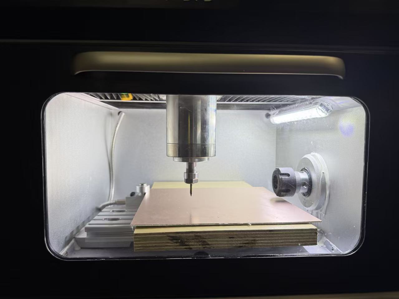
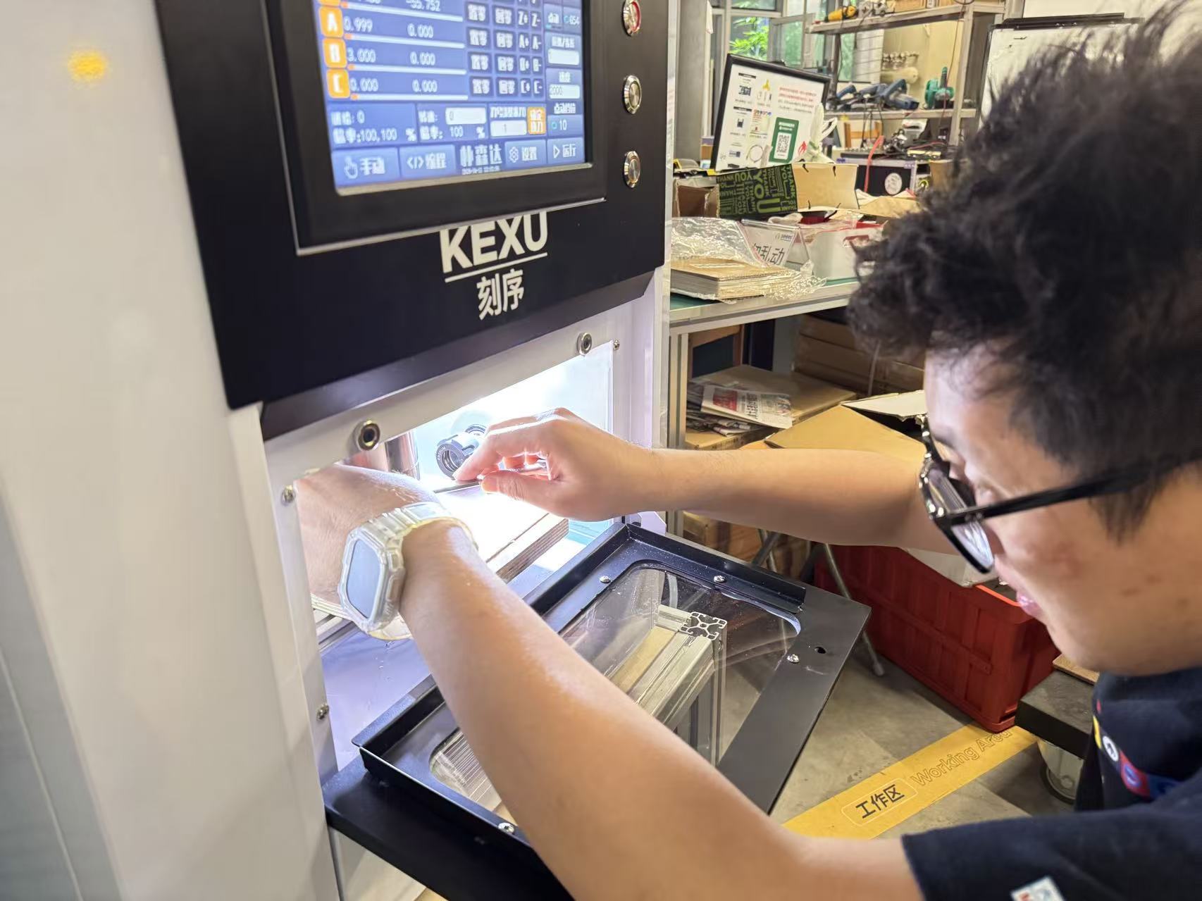
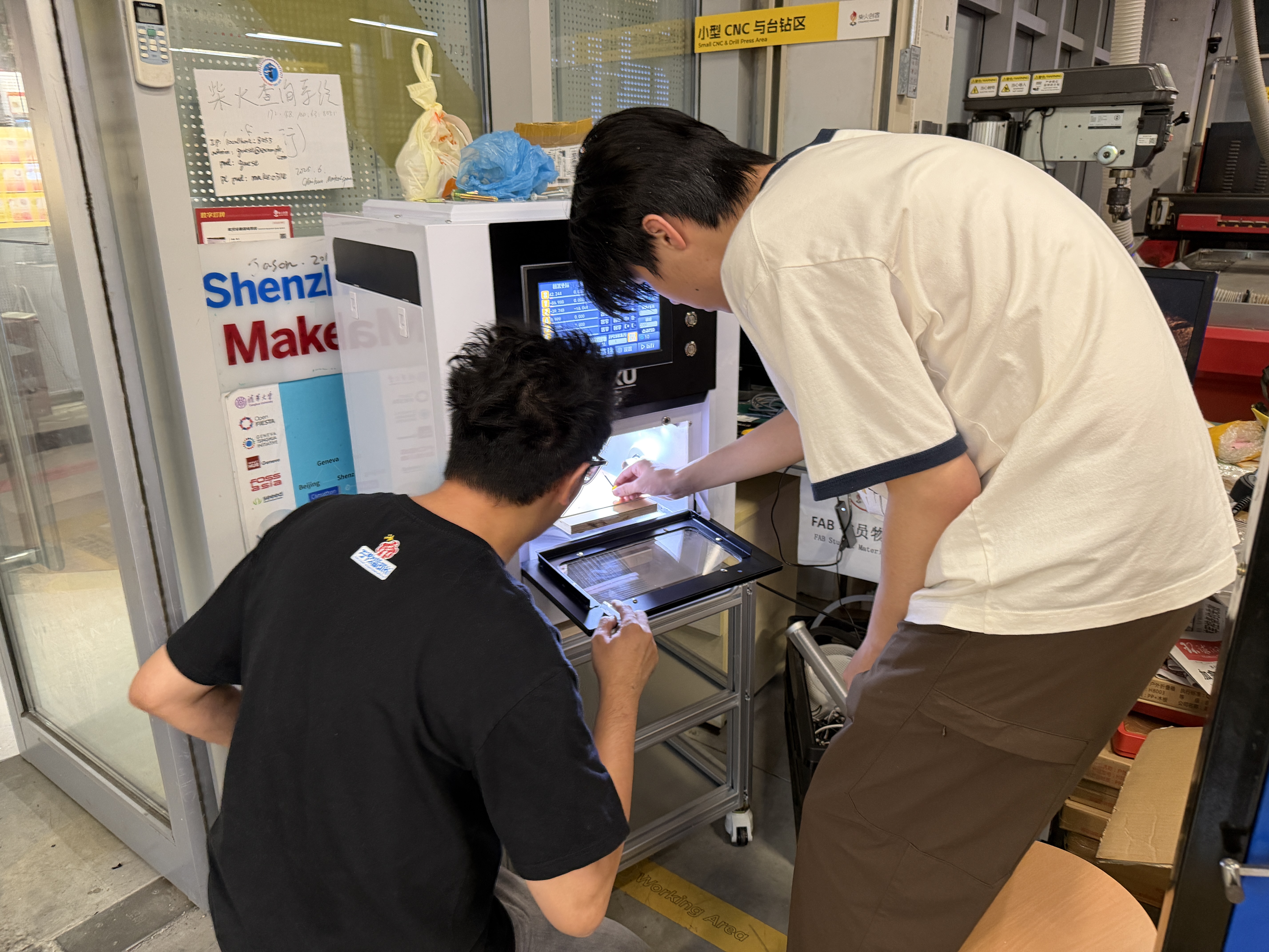
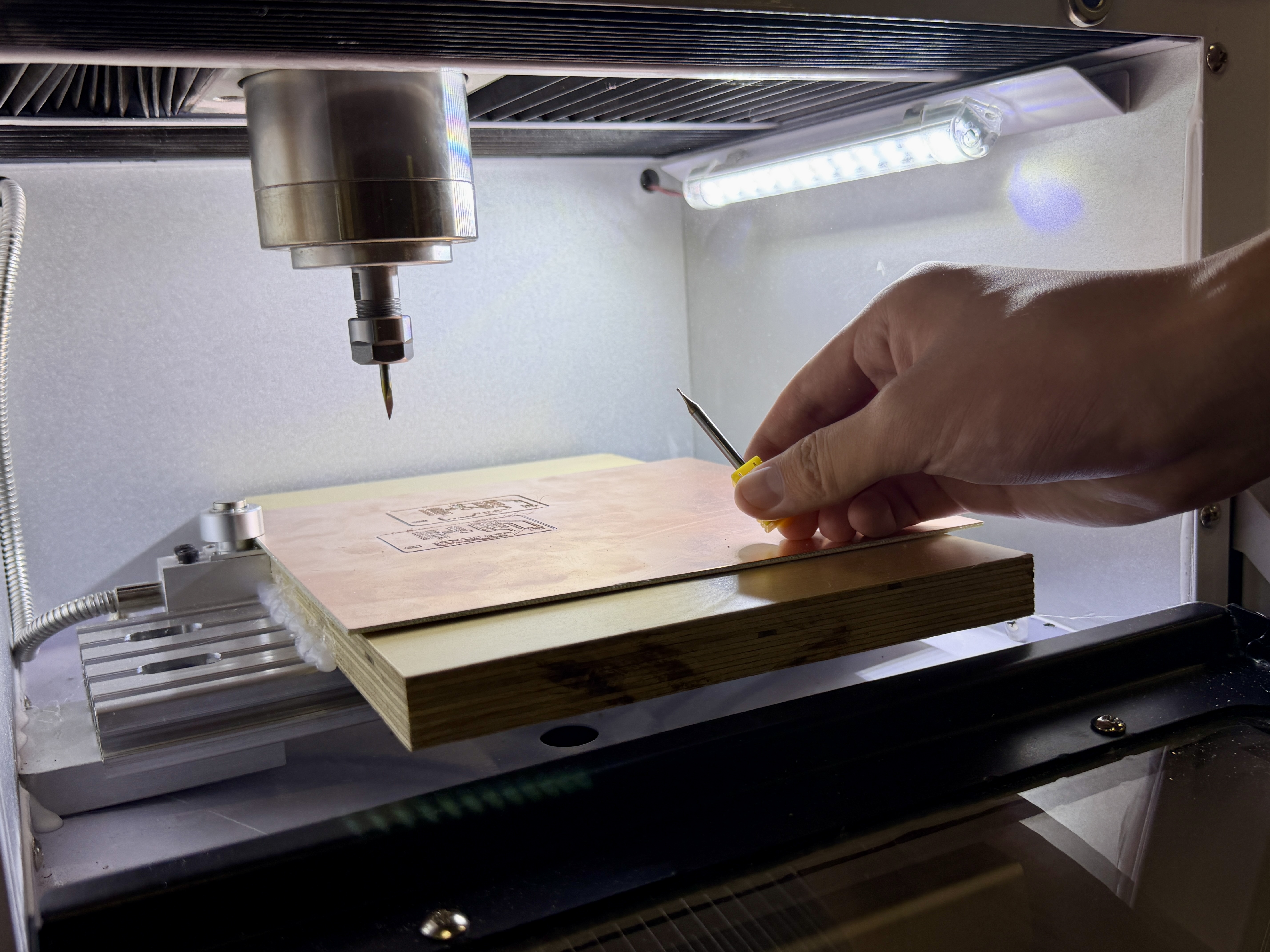
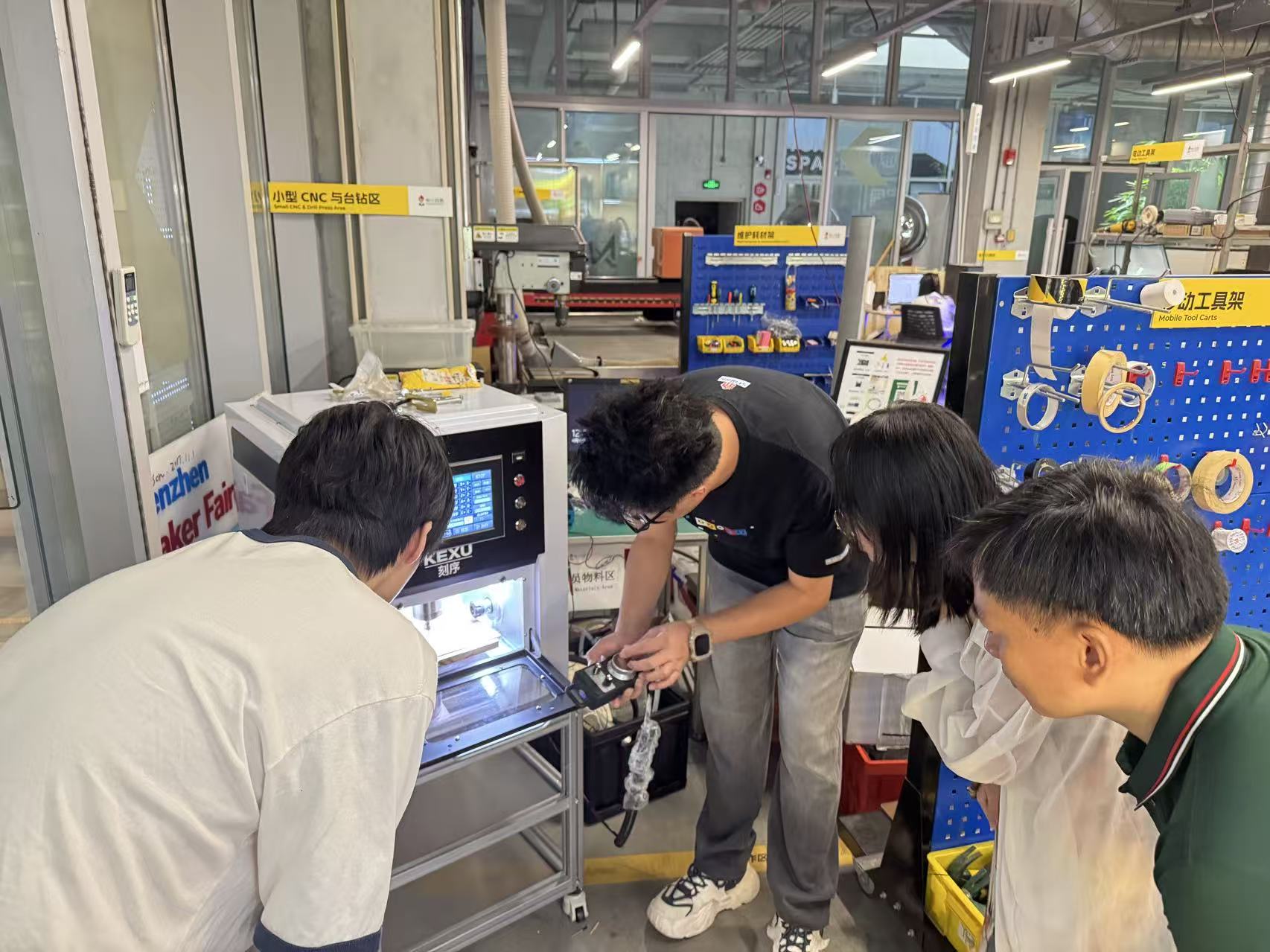
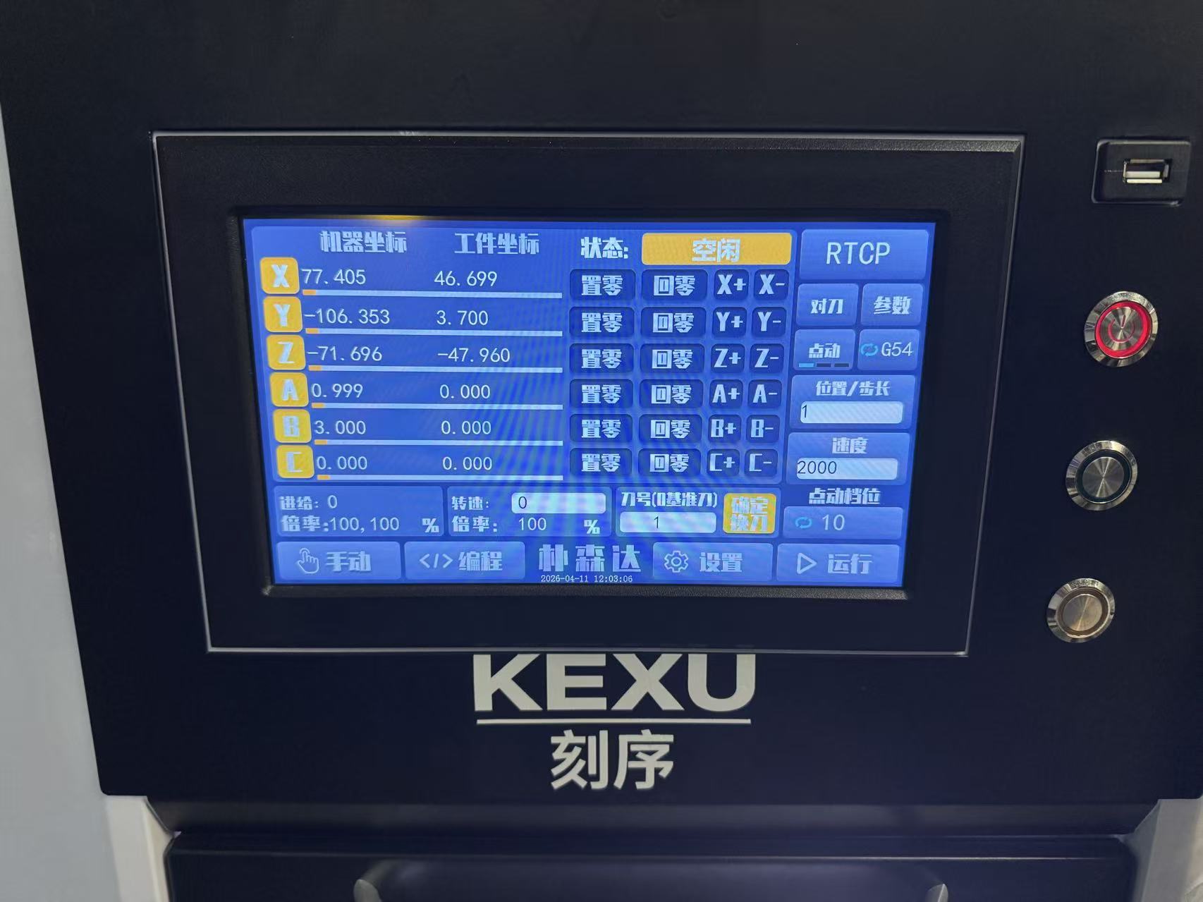
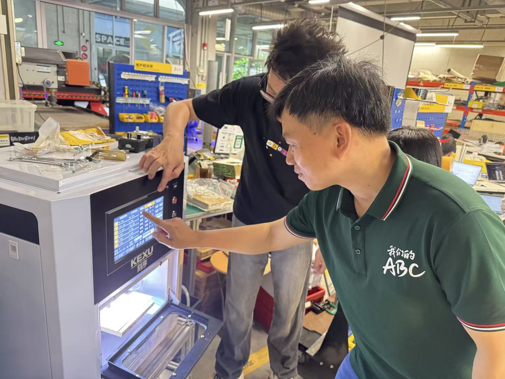
I copied both finished programs to the CNC USB / shop PC, loaded the trace file first, then swapped to the outline file after a tool change. Clamping, touch-off, spindle checks, and safety steps are on the group assignment page; the videos below pick up once the post-processed G-code was running.
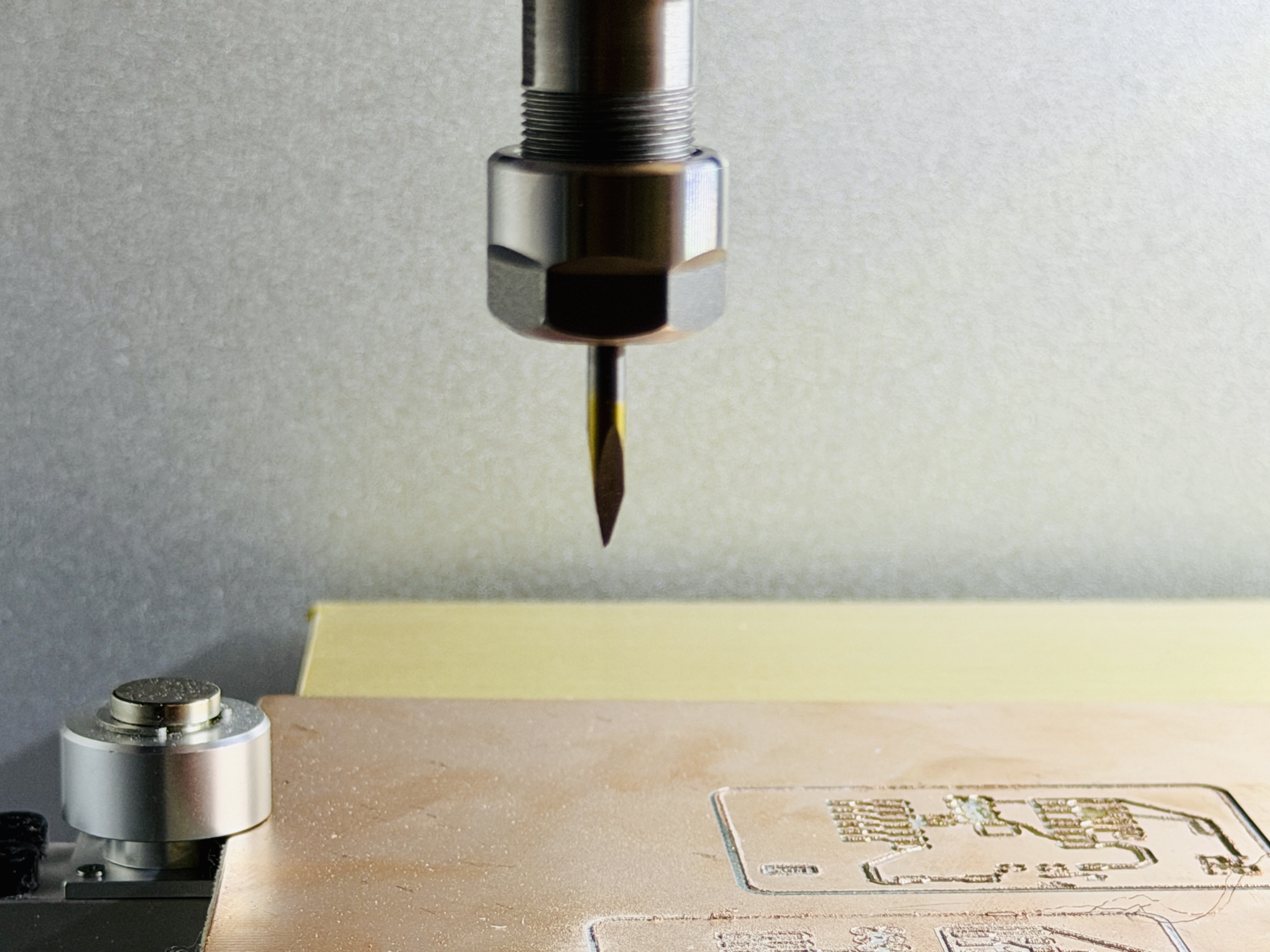
On the mill: run, deburr, inspect
I clamped single-sided copper-clad on the Chaihuo mill and stayed at the machine for the first isolation pass. Feed and spindle sounded rougher than ideal, which showed up on the copper afterward — a reminder to cross-check Mods feeds against the nameplate before the production run.
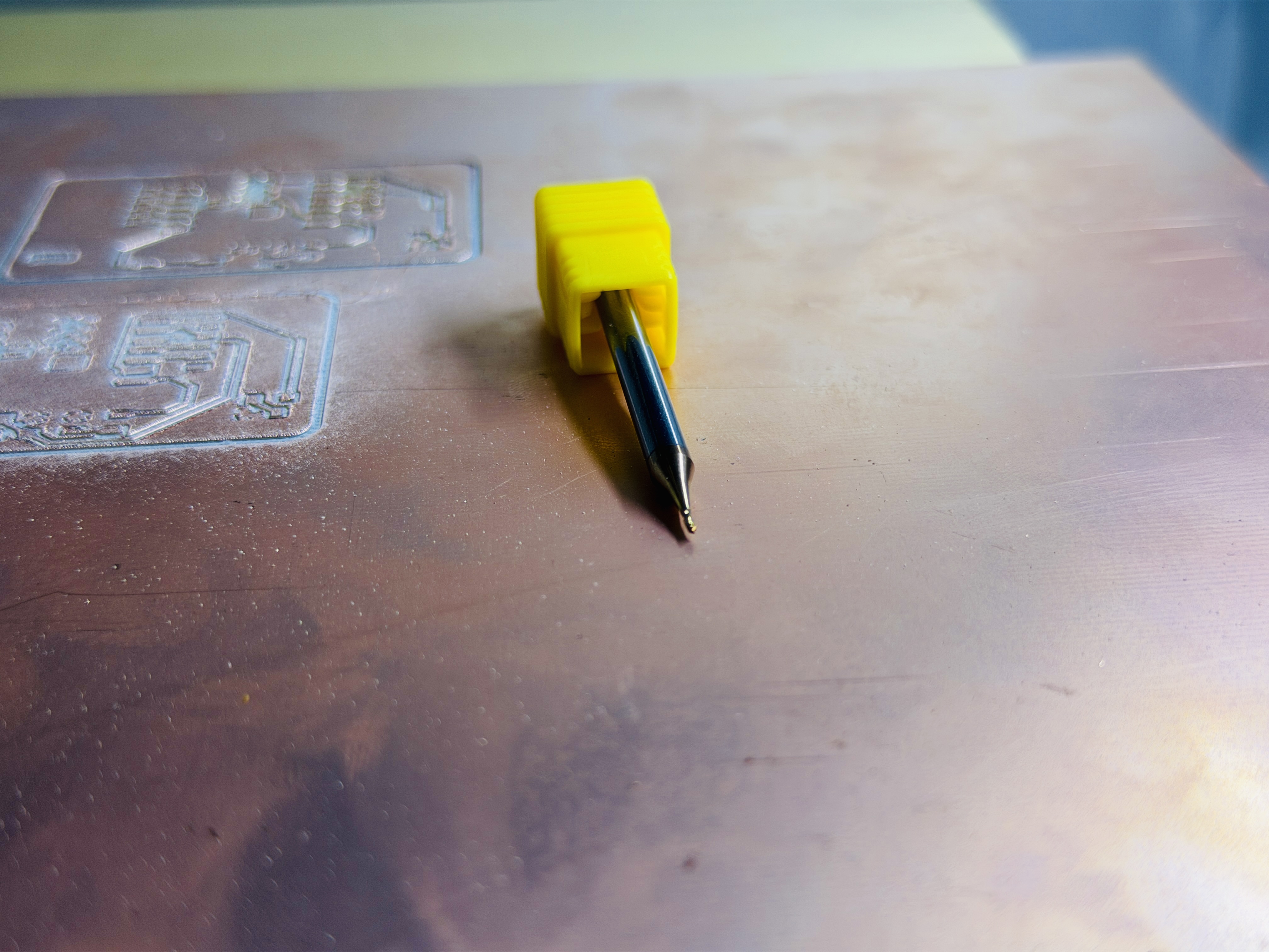
Right off the machine the board looked electrically suspicious. Burrs and ragged copper slivers sat between traces. I think the spindle speed was a bit low for the feed we used, so the bit smeared metal instead of shearing cleanly. Before I dared to solder a module, I lightly sanded the top copper with P800 (~800 grit) sandpaper, brushing along the isolation channels until the slivers were gone and the edges looked matte instead of feathery.
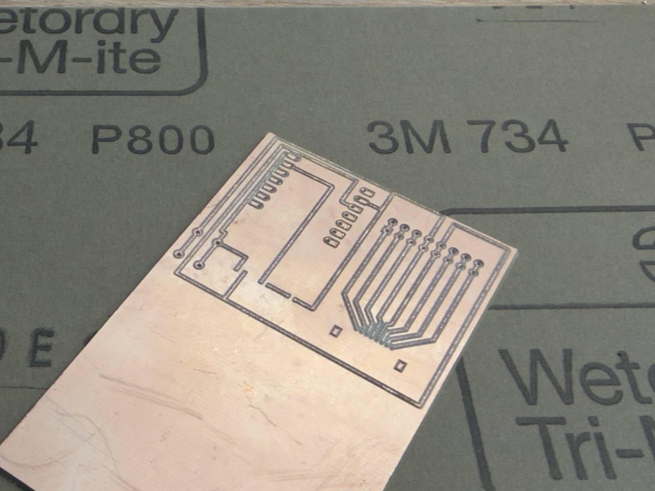
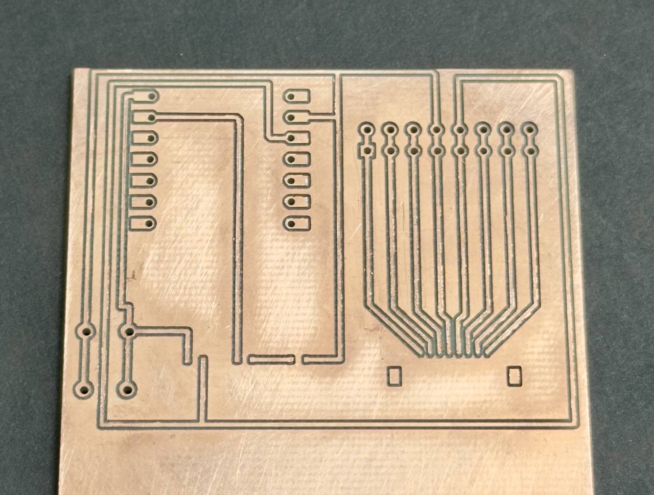
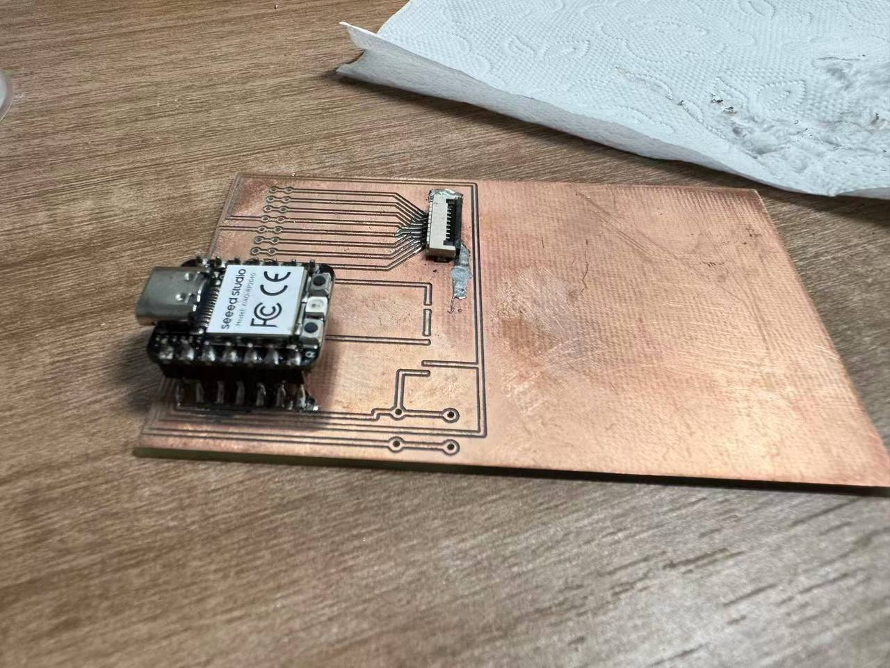
Milled board: deburr, brief solder attempt, continuity
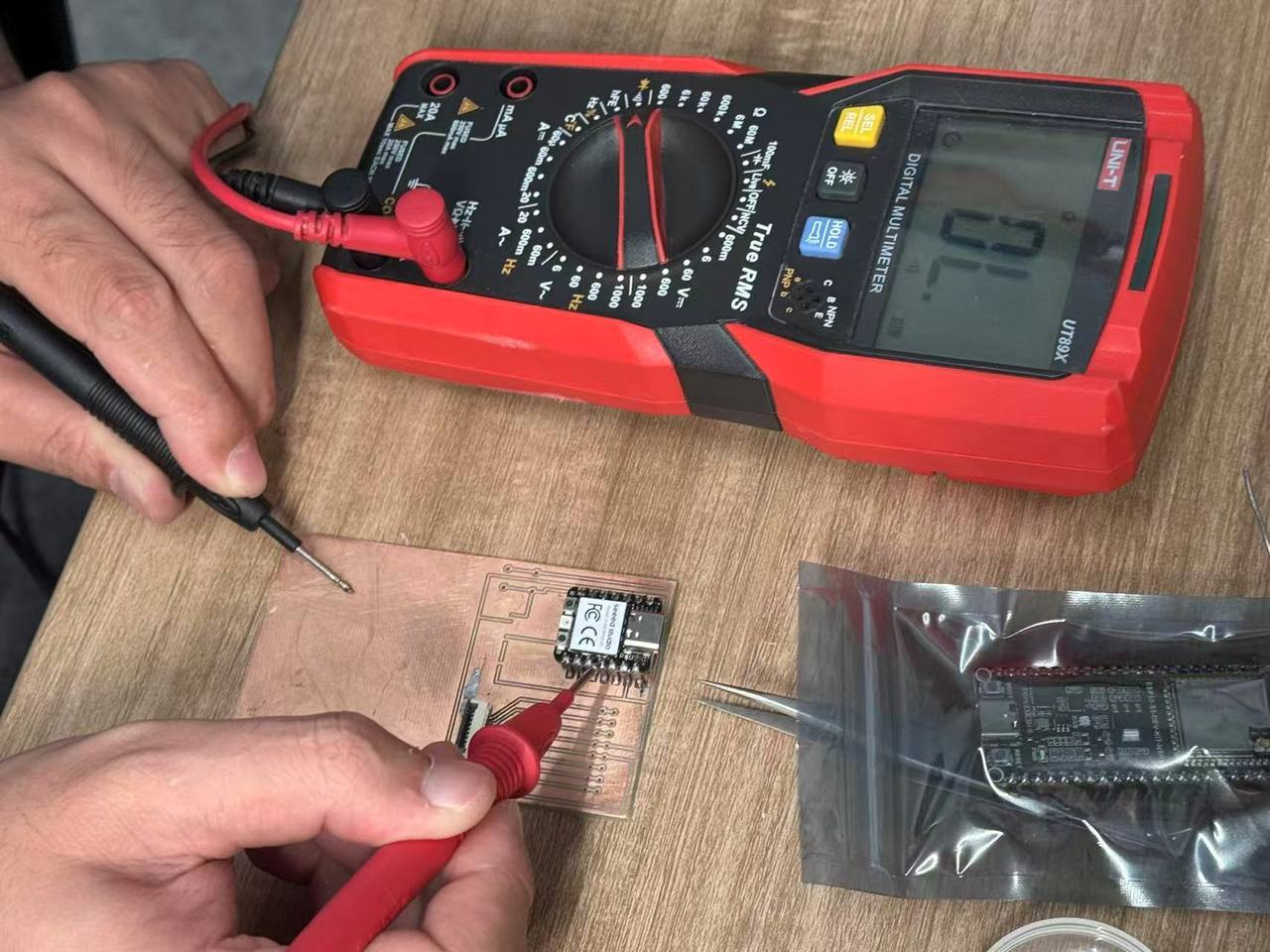
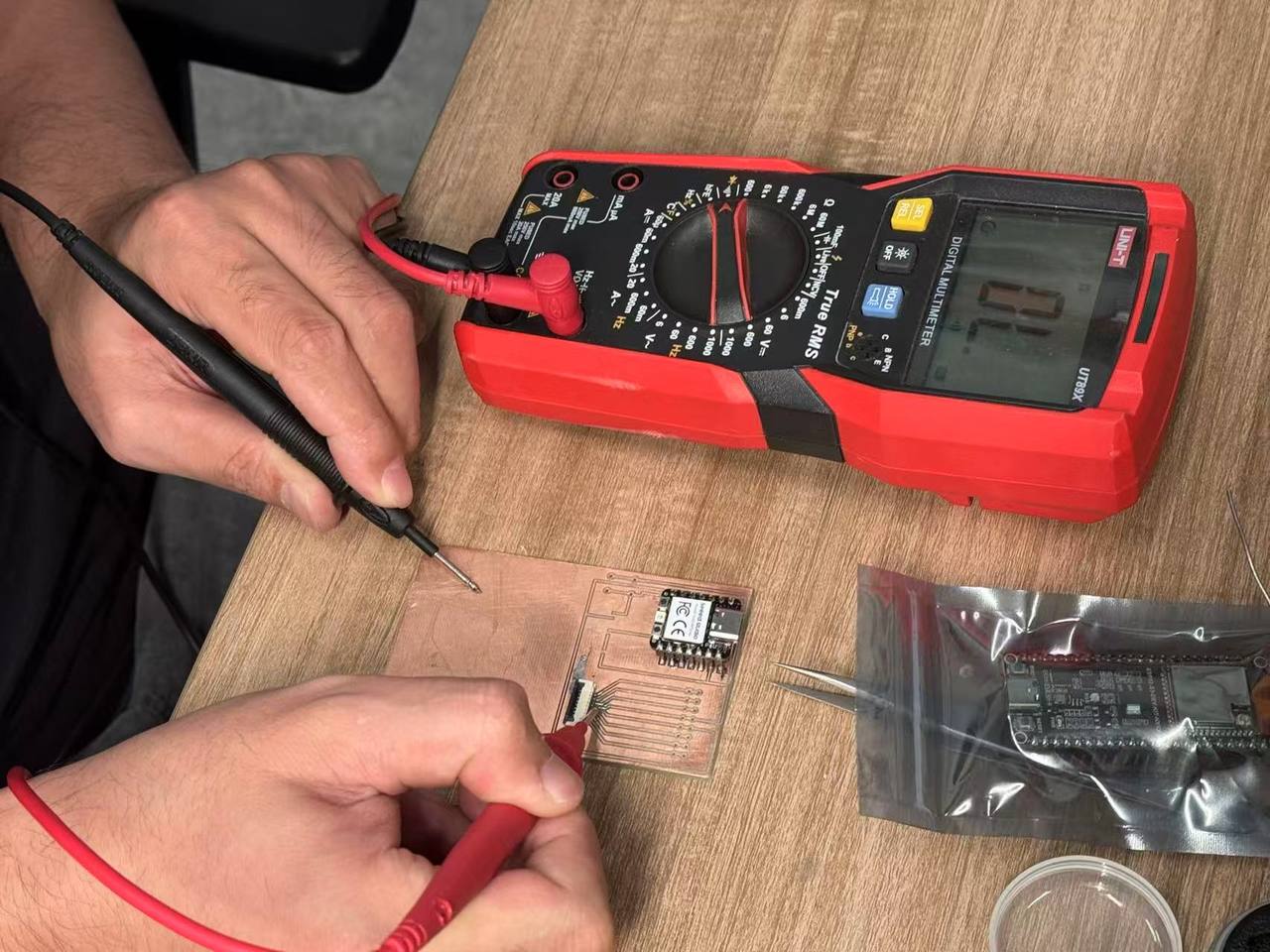
On the milled copy I deburred, tried to tack a XIAO + FPC, and stopped when the castellated pads felt too tight against the isolation. No mask, thin fingers, and leftover burrs made rework risky. I still ran multimeter checks on that board (photos below) to prove the layout was not shorted before abandoning it for JLC assembly.
Before USB power I checked shorts to the ground pour with a multimeter in continuity mode: probe from each connector pad to the surrounding copper fill and to neighboring nets. I did this separately for the XIAO footprint and the FPC pads so a bridged burr would not kill the 3.3 V rail on first plug-in.
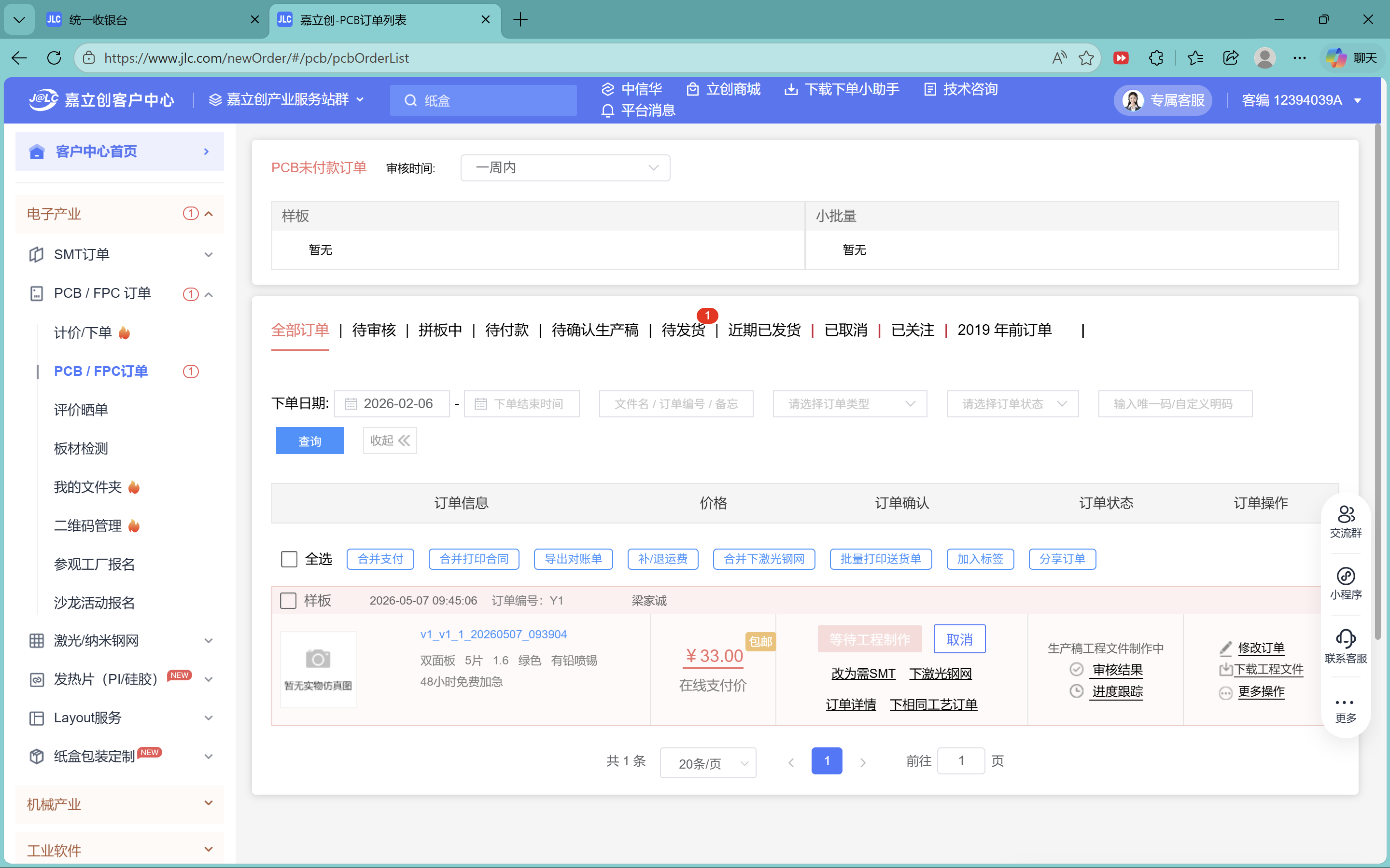
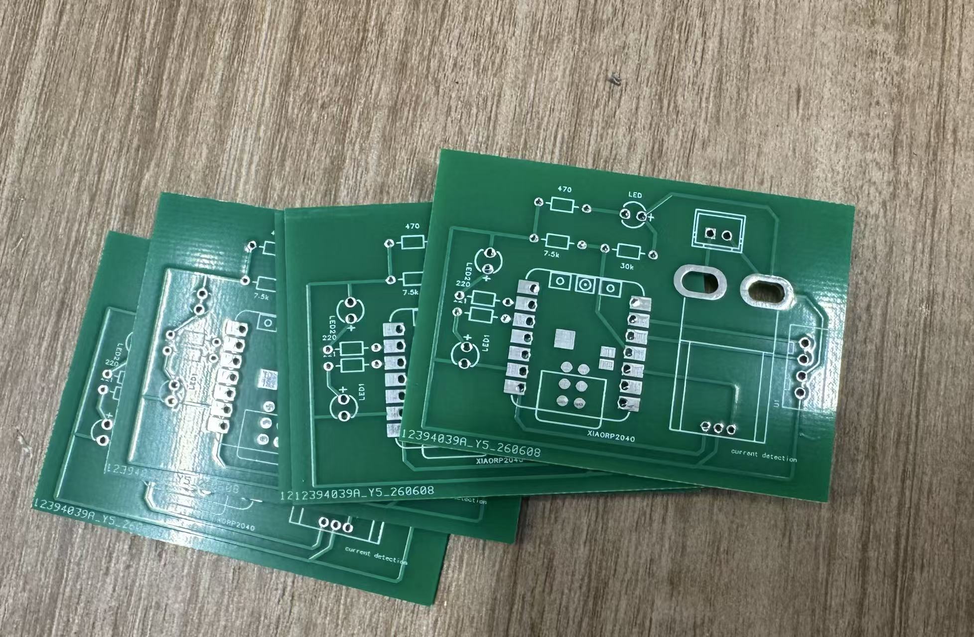
Board house: JLCPCB order, assembly, and functional test
Milling taught me the layout was routable, but the birthday-spirit carrier still needed plated holes, solder mask, and rev 2’s side panel for the NanoStat/Pico stack. I ordered two hub revisions from JLCPCB, plus separate panels for the WROOM display board and the charging-dock board. The hub I stuffed, programmed, and show below is rev 2. The other two boards arrived the same week; I log them here as production evidence even though full assembly waits for packaging (Week 10 WROOM output, final project dock enclosure).
Revision 1: dense layout, no integration margin
I laid out a first PCB that packed the circuit tightly. Electrically it was fine for a first cut, but there was no unused copper area left next to the main circuit where I could later mount a small microcontroller carrier or breakout for sensors. For the birthday-spirit idea I need a predictable place to attach my NanoStat (ESP32 Pico–footprint) board and related sensor hardware without cramming everything into one cluttered copper island.
Revision 2: reserved side area for the Pico module
On the second spin I kept the same core circuit intent but moved outlines and poured/open regions so there is a dedicated blank panel beside the dense logic. That zone is for mechanically attaching (e.g. adhesive standoffs or double-sided tape, pending mechanical review) the NanoStat module without overlapping traces or interfering with reflow on the main section.
Ordering through the JLCPCB desktop client
I uploaded Gerbers through the 嘉立创 / JLCPCB client, checked layer previews and board thickness, then pushed the job through their quoting flow. Keeping filenames and revision notes aligned between EDA and the upload dialog avoided mixing rev1 and rev2 uploads.
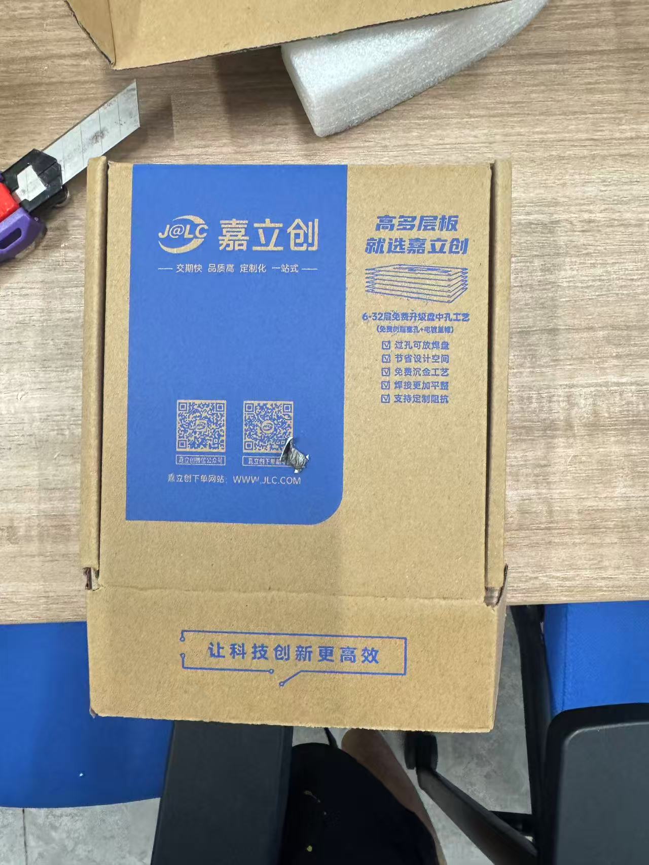
Boards arrived
The fabricated panels showed both revisions clearly; handling them highlighted how much easier plated holes and solder mask make bring-up compared to quick milled copper, especially for dense SMT footprints I plan to assemble next.
Fabricated boards: photos after delivery
The close-ups below are physical boards photographed after the JLC shipment arrived, same revisions as above, shown as fabricated copper and solder mask rather than EDA captures.
WROOM display PCB (board #2): design and fab
Forest Fairy splits sensing from the face. Hub board #1 stays between the chassis and the flowerpot; this leaf-shaped WROOM carrier is board #2. I laid it out in EasyEDA with an ESP32-S3 WROOM footprint, screen harness pads, power input, and decoupling. I plan to solder the WROOM module onto this panel and mount the finished board inside the mobile base (left side of the chassis in my packaging sketch, Week 16). From there it drives the pot-mounted ST7789 over a wire harness and listens for HostLink I²C from the XIAO hub.
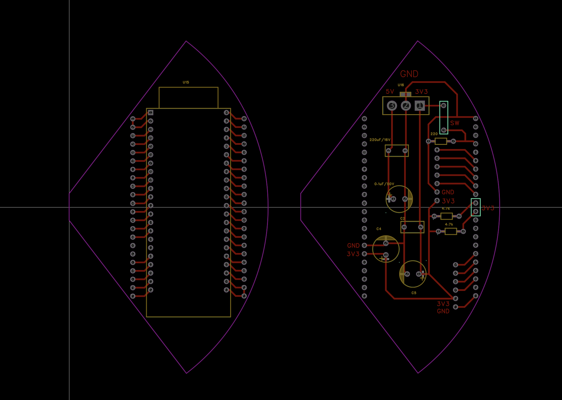
Charging-dock PCB (board #3): design and fab
The robot docks on a separate 充电桩 (charging station). That enclosure needs
its own PCB for dock power, current sensing, and status hardware — separate from the mobile hub.
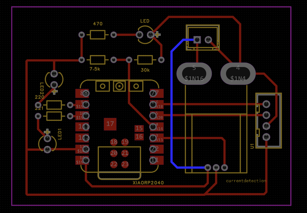
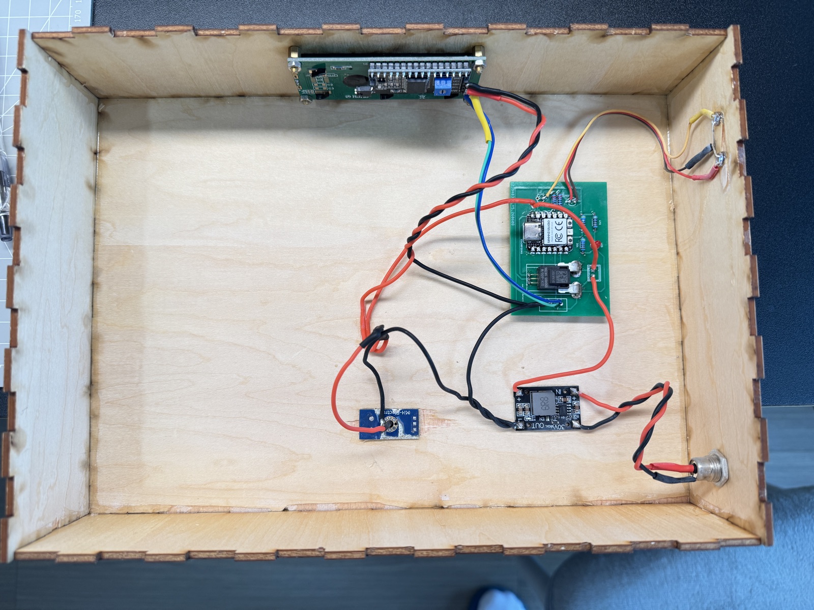
I drew this board in 嘉立创 EasyEDA as a double-layer layout
(双层板): top and bottom copper with plated vias, ordered through the same JLC
batch as the hub and WROOM panels. The schematic centres on a Seeed XIAO RP2040,
a STK-600/M Hall current module (currentdetection), a
30 kΩ / 7.5 kΩ divider on BAT+ for charge voltage, two
status LEDs on D8/D9, and a 4-pin LCD header on
D0–D4. It lives inside the laser-cut dock, not on the robot base;
wiring to the DC jack, magnetic contacts, and front-panel LCD continues on
final-project.html.
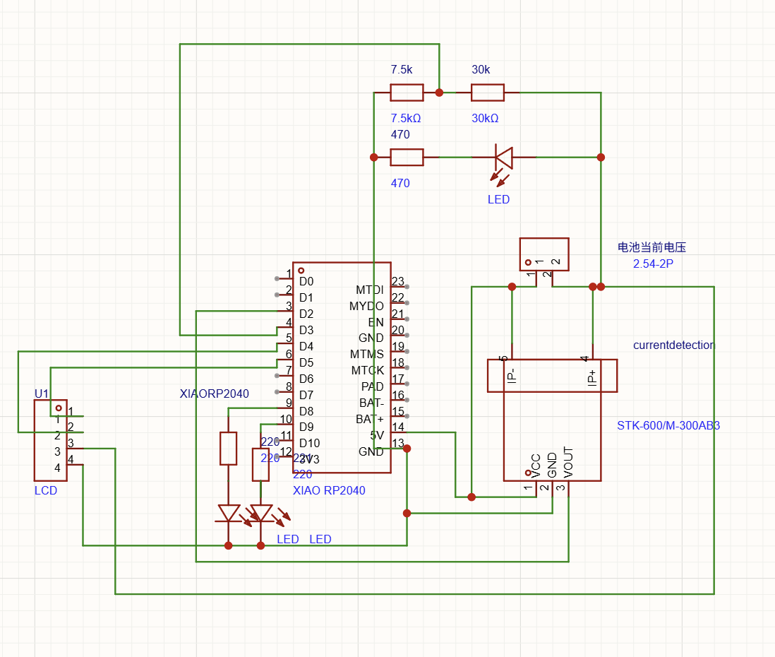
U1, and status LEDs.
currentdetection silk.
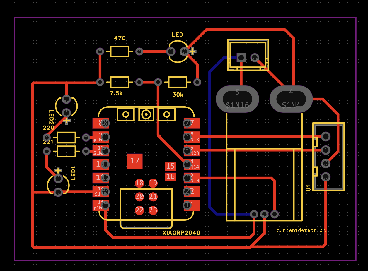
Design file:
design-files/week08/charging-station.eprj2
— 嘉立创 EasyEDA project (double-layer charging dock).
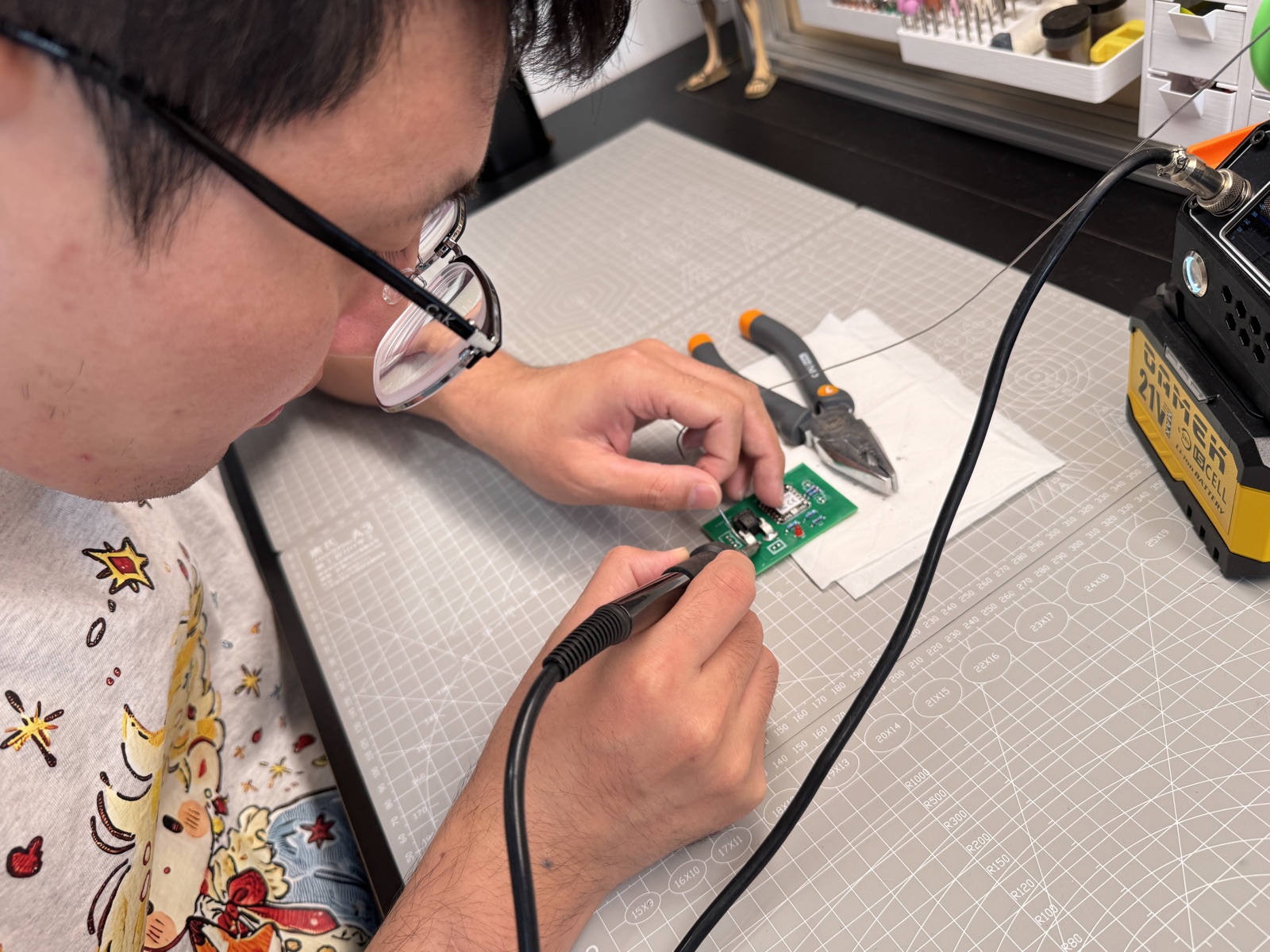
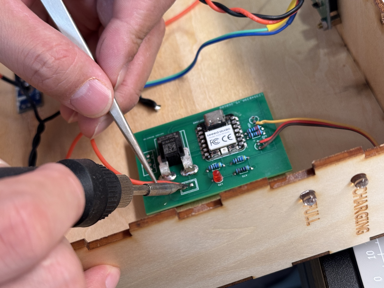
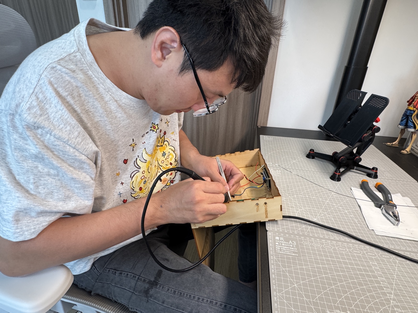
Stuffing and soldering (charging dock)
I stuffed this dock board the same week the panels arrived, using an iron around
330–350 °C, a conical 0.8 mm tip, and no-clean
flux on the green mask. I started with the XIAO RP2040, aligned it to the
footprint, tacked opposite corners, and then flowed each castellated pad without bridging its
neighbour. The STK-600/M current module needed more heat because the large
through-hole sensor has both mechanical tabs and signal pins, so I held the body with pliers
while tinning each leg. After that I soldered the passives and LEDs, including
470, 7.5 k, 30 k, and 220
resistors, then meter-checked the divider before powering the XIAO. Only after the PCB passed
continuity did I mount it in the finger-joint box and run power, sensor, and LCD leads to the
side-panel jack and magnetic contacts.
Programming: USB upload and live serial proof
The board I designed and assembled also had to run a program, not just pass continuity. On
the JLC rev 2 panel I first used
code/week08-xiao-bringup.ino as a
smoke test in the Arduino IDE, with board set to XIAO ESP32S3 and Serial
Monitor at 115200 baud. That sketch blinked the user LED and printed
[Week 8] Carrier alive, which told me USB upload, reset, and serial were alive.
After that I moved to the integrated hub firmware: the XIAO runs
s3-upload/src/main.cpp
with
pico_stat_bridge.cpp,
while the Pico sidecar runs
pico-upload/src/main.cpp
and sends STAT,… lines over UART. The useful proof is on the XIAO USB port:
Serial Monitor shows those lines forwarded with the [PICO RX] prefix.
Upload flow: connect USB-C to the soldered XIAO → select the CDC port → upload → open Serial
Monitor at 115200 baud. Pass criteria for Week 8: repeating
[PICO RX] STAT,ver=1,valid=1,…,reason=ok,… lines — proof the programmed hub
talks to the Pico sidecar on the same PCB I stuffed.
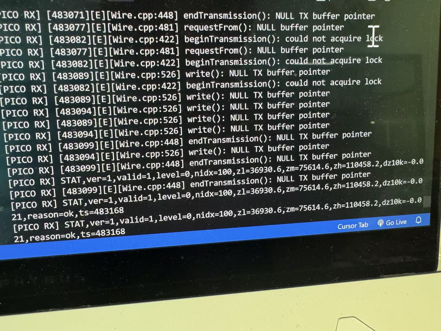
[PICO RX] STAT,…,reason=ok — UART bridge
working on the JLC rev 2 board. Early Wire errors were from bring-up
before I²C sensors were connected; the STAT stream is the functional output I kept for
assessment.
DHT11 + light sensor reads on the same carrier continue in
Week 9 (
week09-s3-serial-env.ino).
I used Cursor to draft the bring-up sketch and the integrated hub / Pico bridge firmware in
week08-xiao-bringup.ino and
final-project-upload/s3-upload/. I still checked pin
names against the JLC board, uploaded over USB, and fixed UART issues from Serial Monitor before calling the hub
working.
5. Conclusion
I now have both production paths on one page. The milled run proved the Week 6 layout is routable and caught a wrong Mods preset (V-bit instead of 1/64″ flat). I did not re-mill; deburr and continuity on that copper were enough process evidence. The JLC rev 2 board is the one I soldered, programmed, and kept for the final project hub. Removable Pico fly wires are a practical compromise: I can flash the sidecar without desoldering the UART/power pins the hub needs at runtime.
Next time I would either widen milled clearances or skip milling entirely for castellated modules this dense. For rev 3 I might route the Pico header to a small socket instead of dupont leads, but the plug/unplug workflow is good enough for now. The WROOM panel waits for Week 10 output work; the charging-dock board is stuffed and wired in the dock box (see dock soldering). Hub rev 2 remains the live firmware target for on-robot sensing.
The evidence I would point to on this page is the full
Gerber → PNG → Mods → post-processed G-code path, the single
lab milling run with deburring and continuity checks, the
charging-dock assembly, and the hub programmed
on JLC rev 2 with serial proof. The source is linked
beside the proof, including week08-xiao-bringup.ino
and the hub + Pico firmware. The board-house workflow is also documented from JLC client upload
through delivery for the hub, WROOM, and charging-dock boards, with the shared Chaihuo mill notes
kept in the group assignment.
Group assignment
Guangzhou (Chaihuo) group documentation: in-house PCB fabrication on the lab CNC mill (operating notes and safety).
In-house PCB fabrication, CNC milling: operating notes
Equipment: Lab PCB CNC mill / engraver (single-
or double-sided copper-clad stock, isolation routing plus outline cutting;
exact model checked from the nameplate and local training).
Use case: Quick-turn prototypes, coursework boards, small
batches; it does not give a professional fab’s plating,
solder mask, or surface finish.
Overview: The process uses a small-diameter end mill to cut isolation channels in copper. A separate pass can cut the board outline. Design data must match tool diameter, cut depth, and work zero; mismatches often cause opens, shorts, or dimensional errors. Minimum trace width, spacing, and tool specs are defined by your lab’s published rules.
I. Recommended operating sequence (aligned with on-site steps)
Our lab workflow was simple: secure stock and tool, set zeros, then run the toolpath.
1. Prepare machining data and verify
- Finish schematic and PCB layout in an EDA tool (e.g. KiCad, Altium, Eagle), then export Gerber (copper, outline, drill layers as required) and drill files; if the lab uses dedicated CAM software, merge layers and set the origin per its instructions.
- In CAM, confirm units (mm), mirroring (top copper on a single-sided board is usually not mirrored; bottom copper per software guidance), and trace-width compensation against the actual tool diameter.
- Check that the outline is closed and does not conflict with fixture keep-out zones.
(This step is done at the computer; no floor photo.)
2. Load and secure the copper-clad board
- Clean the table and the underside of the stock so chips do not cause warp or uneven thickness.
- Place the board within the machine’s usable travel, with clearance for clamps and the toolpath; for double-sided work, plan dowel or optical alignment if the lab provides it.
- Clamp with lab-approved fixturing with enough holding force, and ensure clamps / bolts stay outside the toolpath envelope.
3. Change the tool (end mill, V-bit)
- Install or remove tools only with the spindle fully stopped and the machine in a safe state (per lab procedure).
- Seat the tool for the collet type and tighten to the specified torque; check flute length and stick-out for enough reach without excess overhang that causes chatter.
- Match the tool diameter to the CAM settings (common isolation milling uses roughly 0.1 mm to 0.2 mm cylindrical end mills; confirm against lab inventory).
4. Position the cutter
- Jog the tool to a safe height above the board so rapid moves cannot hit the stock or clamps.
- Align the tool roughly with the programmed origin (board corner or locating feature) to match the CAM work coordinate system.
- Confirm the dust shoe, guards, tool length, and clamps do not interfere.
5. Touch off and set work zero
- XY zero is often a board corner or locating feature and must match the CAM origin definition.
- Z zero is often on the top of the copper-clad surface or a lab-defined reference; Z error yields shallow cuts (copper not fully cleared) or deep cuts (substrate damage, broken tool).
- The two images below show the initial state before touch-off and zero-related steps; the exact method (touch plate, shim, paper drag, etc.) follows on-site training.
6. Test cut and production run
- For a new file, use a reduced feed override or single-block mode first and watch whether the first isolation pass fully clears copper and whether the sound is normal.
- The operator must stay at the machine; on any fault, hit emergency stop immediately.
- After the run, inspect for residual copper and burrs between traces; deburr if needed and spot-check continuity with a multimeter.
II. Safety and precautions
- Personnel and motion: Do not clear chips by hand near a running spindle; do not wear gloves on rotating parts; tie back long hair; know where the emergency stop is.
- Tool and workholding: A loose tool or loose board can eject; after each load or tool change, push gently to verify the board cannot shift.
- Dust and copper swarf: Use dust collection; avoid inhaling copper dust; stop the machine before cleanup.
- Electrical: Do not touch electrical parts with wet hands; route cables away from moving parts.
- Program and coordinates: Mismatched zero, tool diameter, stock thickness, and CAM data is a common cause of shorts, opens, and crashes; after a board change or tool change, re-touch off or re-verify Z.