Week 9: Input devices
Input devices week. The group work looked at what signals actually do on copper and wire (slow ramps, noisy edges, decoded buses). For my individual assignment I documented two analog input paths on boards I designed: (1) the Week 8 JLCPCB hub with a light sensor and DHT11 on the Seeed XIAO ESP32-S3; (2) the Forest Fairy charging dock with a DFRobot Gravity 50 A current module plus a resistor divider for charge voltage — both read through ADC pins and logged on serial at 115200.
Individual assignment: input devices on my PCB
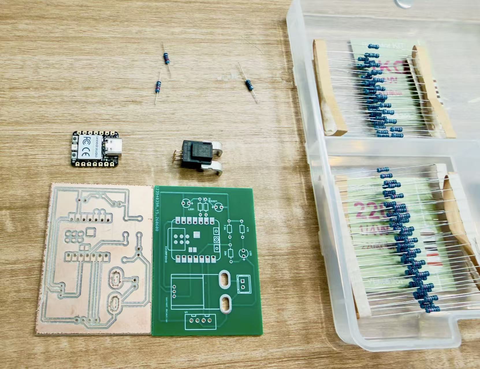
Fab Academy Input Devices asks me to measure something: add a sensor to a microcontroller board I designed and read it. The module FAQ also says the assessed interface should not stay on a breadboard, so this week I used the board provisions from my electronics-design work: MCU pads, sensor signal/power pads, and off-board harness points. I covered two carriers from the same final project — the sensor hub and the charging dock — both fabricated in Week 8.
Board context (Week 8) vs scope (Week 9)
The fabricated board from Week 8 is meant to host two compute / sensor blocks on one panel: a soldered Seeed XIAO ESP32-S3 and a mechanical landing zone for a NanoStat module (ESP32 Pico–class footprint, reserved in revision 2 for final-project plant impedance work). The important Week 9 point is that the board already provides sensor connections: 3.3 V, GND, one DHT11 digital data net, and one light-sensor ADC net routed to the XIAO side.
I kept Week 9 evidence on two tracks. On the hub I show the XIAO reading light and humidity/temperature from parts soldered on the same PCB. On the dock I show a Seeed XIAO RP2040 reading charge current from a Hall module and charge voltage from a divider, then printing both on USB serial. The final-project upload later adds the Pico/NanoStat plant-impedance node; I archive those source files below so the full data path is visible.
1. Task
For my birthday-spirit final project I need environmental sensing near the plant and power telemetry on the charging dock. This week I proved both input paths on fabricated copper rather than treating them as breadboard tests.
Sensor hub (XIAO ESP32-S3)
The MCU will not sit in the same enclosure as the light and DHT heads, so I landed those transducers on the Week 8 hub, read them through the XIAO, and mirrored values on a small UI while tuning placement. The NanoStat site stays unused for now.
On the sensor hub, the inputs in scope were the DHT11 humidity / temperature sensor on D2 (GPIO3) and the photoresistor-style light divider on D3 (GPIO4). The XIAO ESP32-S3 is soldered on the Week 8 PCB and reads both through its 3.3 V GPIO / ADC pins. I left the NanoStat footprint empty this week: no module, no firmware, and no layout change. The rainbow ribbon is intentional because the light and DHT11 heads need to move to better locations in the final enclosure while the PCB remains the hub.
Charging dock (XIAO RP2040)
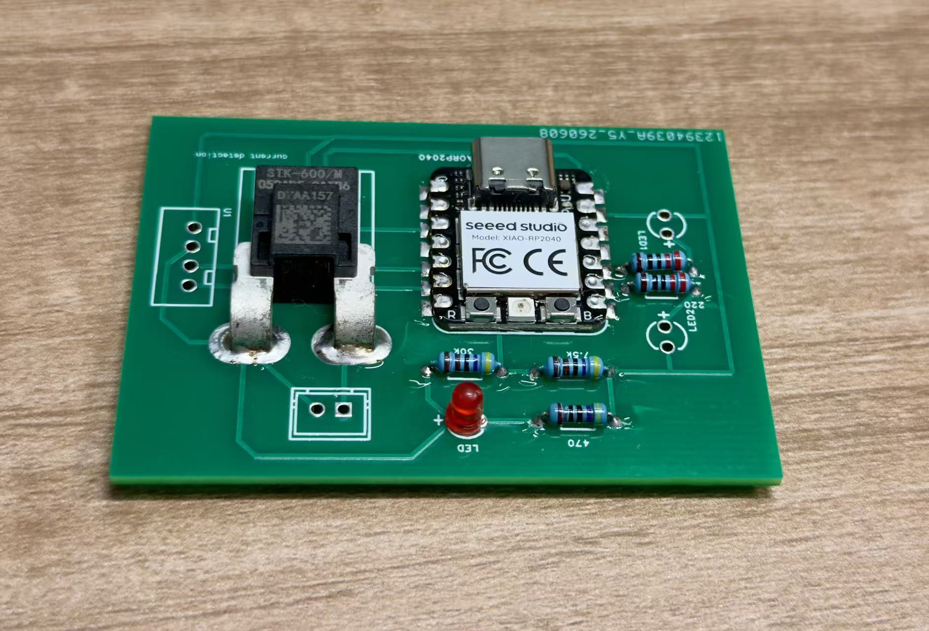
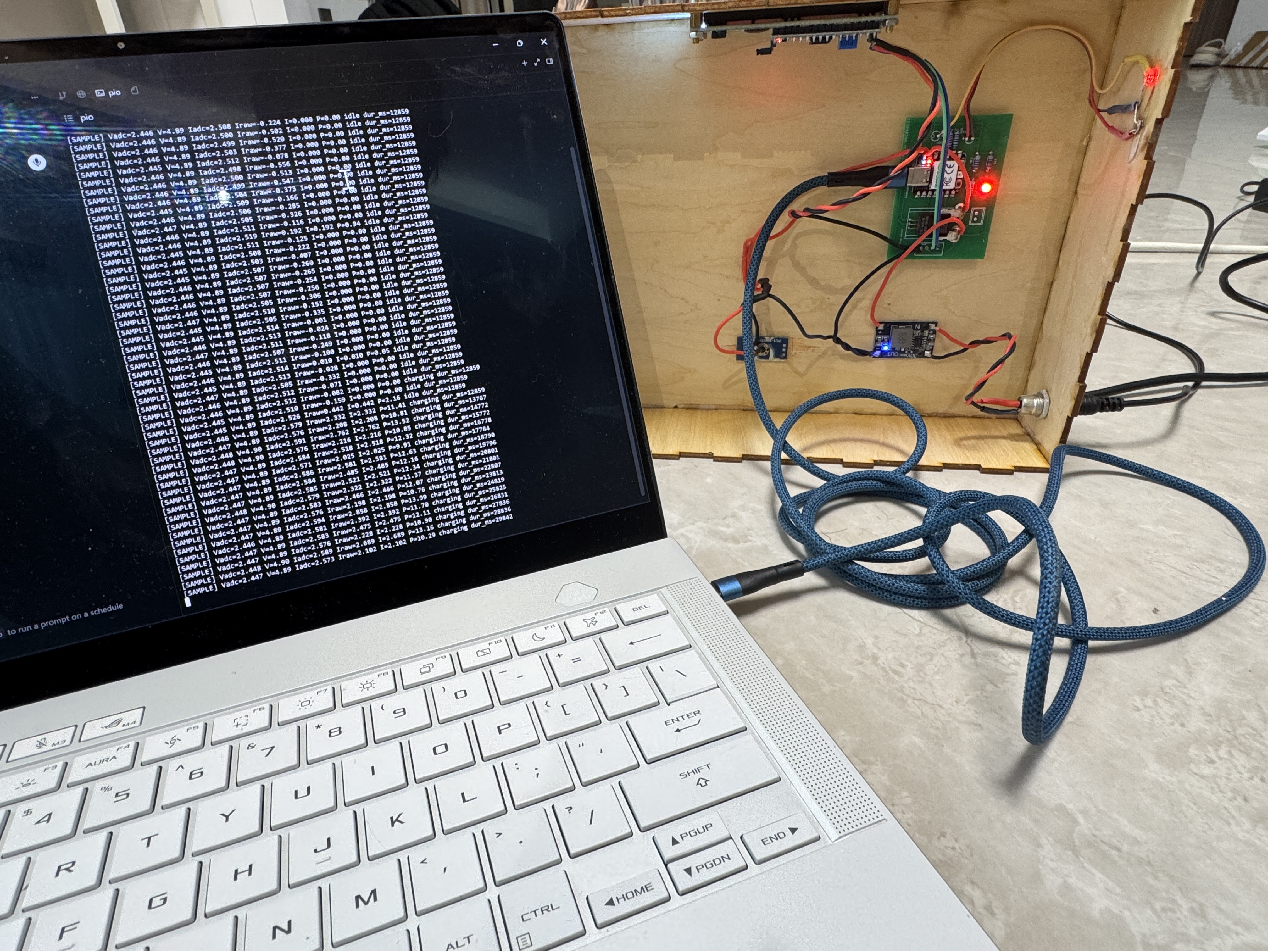
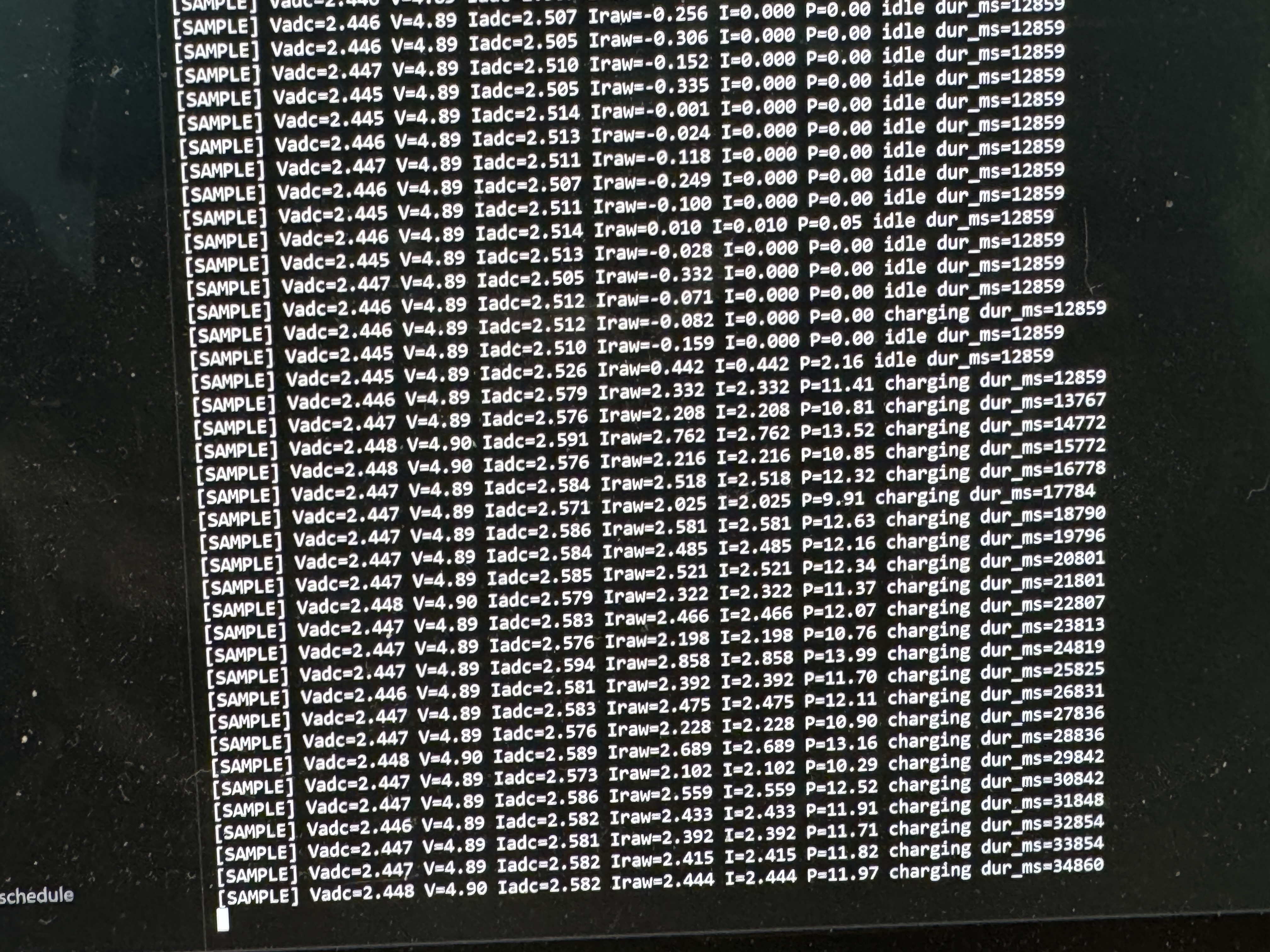
The dock needs to know whether a robot is drawing current and what voltage is present at the pogo contacts. I soldered the Week 8 charging-dock PCB, wired a Gravity 50 A analog current module (SEN0098-V2, STK-600/M Hall sensor) to A2, and routed the charge bus through a 1:2 resistor divider to A3. Firmware averages 16 ADC samples per channel, applies the divider and Hall linear formulas, and prints voltage, current, power, and charge duration on serial at 115200 8N1.
On the charging dock, the measured inputs were the Hall module analog output on
A2 (GPIO28) and the divider tap on A3 (GPIO29). Firmware
calculates current with
I = (VA2 − Vzero) / sensitivity and charge voltage with
Vcharge = VA3 × 2, because the hardware divider halves
the rail before it reaches the ADC. The LCD and status LEDs are outputs, so I mention them
only as context; Week 9 evidence is the analog input read and the serial log from the
Seeed XIAO RP2040 on the dock PCB.
Connection diagram
This is the same system layout I later used in Week 11, expanded here to make the input-device connections explicit. For Week 9 the key connections are the two sensors on the XIAO hub (D2 / GPIO3 DHT11, D3 / GPIO4 light) and, on a separate board, the dock ADC inputs (A2 current, A3 voltage divider). Power and ground are shared across modules whenever data lines cross between boards.
flowchart LR
  DHT["DHT11 humidity + temperature sensor
VCC 3.3 V / GND / DATA"]
  Light["Light sensor divider
3.3 V - LDR - ADC tap - resistor - GND"]
  Xiao["Week 8 JLCPCB sensor hub
Seeed XIAO ESP32-S3"]
  Pico["ESP32 Pico + NanoStat
plant impedance input"]
  Wroom["ESP32-S3 WROOM UI board
ST7789 + FT6336"]
  Display["Environment / Plant pages
live values on screen"]
  Uno["Arduino UNO motion node
later final-project output"]

  DHT -- "DATA -> XIAO D2 / GPIO3
single-wire timed digital signal" --> Xiao
  Light -- "ADC tap -> XIAO D3 / GPIO4
12-bit analogRead()" --> Xiao
  Xiao -- "I2C master: SDA D4 / GPIO9
SCL D5 / GPIO8, addr 0x55" --> Wroom
  Pico -- "UART1 115200 8N1
Pico TX GPIO1 -> XIAO D7 / GPIO44" --> Xiao
  Wroom --> Display
  Wroom -- "UART1 9600 8N1
WROOM G45 TX / G35 RX" --> Uno
2. Learning
I re-read the academy sensing notes and the DHT11 timing diagram. The humidity chip is not “I²C simple”: it needs a strict start pulse and bit sampling on one pin. The light path is the opposite problem, essentially DC from a divider, so I watch reference voltage, ADC resolution, and noise from the USB front-end.
Group work this week ( below) showed that slow analog looks boring on a scope until you zoom in, while one-wire sensors fail quietly if the wire is loose. Both mattered when I moved from jumper tests to soldered leads.
Working principle of the sensors
The DHT11 is a digital humidity/temperature sensor. It measures RH and temperature internally,
then sends calibrated bytes over one data line. I use the Arduino DHT library on
GPIO3 for the start pulse and bit sampling, then read
readHumidity() and readTemperature(). If either value is
NaN, the sketch treats that sample as a failed read instead of printing a fake
number.
The light sensor is a voltage divider. The photoresistor resistance drops as light increases,
so the tap voltage moves. The XIAO reads GPIO4 with a 12-bit ADC. Firmware keeps the raw count
for debugging and maps it to a percentage with 100.0 * adc / 4095.0. That is not
a lux meter; it is a repeatable brightness input for deciding whether the plant area is dark or
bright.
Charging dock: Hall current module + voltage divider
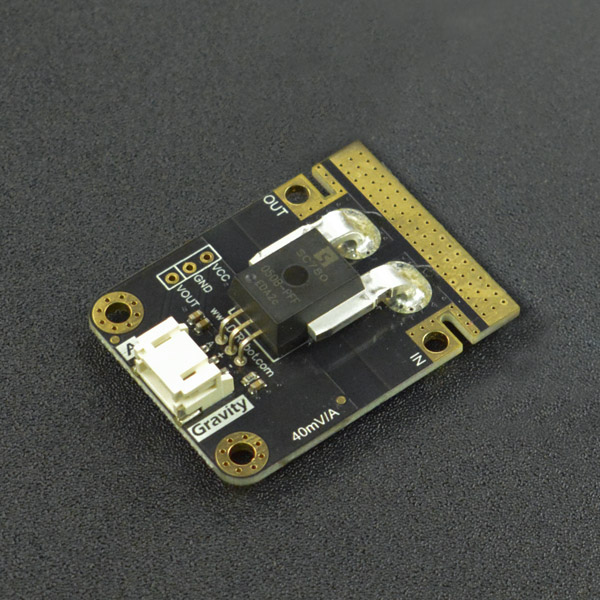
The dock uses a
DFRobot Gravity 50 A (AC/DC)
current module (part SEN0098-V2). It is built around an STK-600/M Hall-effect linear
sensor: the module outputs an analog voltage that moves roughly linearly with
bus current (±50 A range, ~120 kHz bandwidth). That is an isolated measurement — the
high-current path does not share ground with the MCU sense path the way a shunt resistor would.
I feed the signal into the XIAO RP2040 12-bit ADC on A2 and treat zero amps as
a non-zero resting voltage (Vzero), then subtract before dividing by
the calibrated V/A slope.
Charge voltage is higher than 3.3 V, so the dock PCB includes a resistor
divider (ratio 1:2) on A3. Firmware reads the tap, converts the ADC
count to volts at the pin, then multiplies by 2 to recover the rail:
Vcharge = (ADC / 4095 × 3.3 V) × 2. I average 16 samples per
channel before converting so USB noise does not flicker the printed values.
3. Plan
I used the Week 8 JLCPCB board as-is, with the XIAO pad populated and
the NanoStat keep-out left empty. The first job was to solder the light front-end and DHT11,
then bring out signal, power, and ground on rainbow wire with some strain relief at the board
edge. Before flashing firmware I matched the nets to the silkscreen: D2 for
DHT11 data and D3 for analog light. Then I uploaded a minimal XIAO read loop,
checked serial first, and mirrored the same values on a display so I could move the sensor
heads and watch placement effects. On the dock PCB I soldered the XIAO RP2040, mounted the
Gravity current module, checked that A2 and A3 stayed below 3.3 V, flashed the
charging_dock
firmware, and used the serial voltage / current / power lines as the pass test.
4. Build and readout
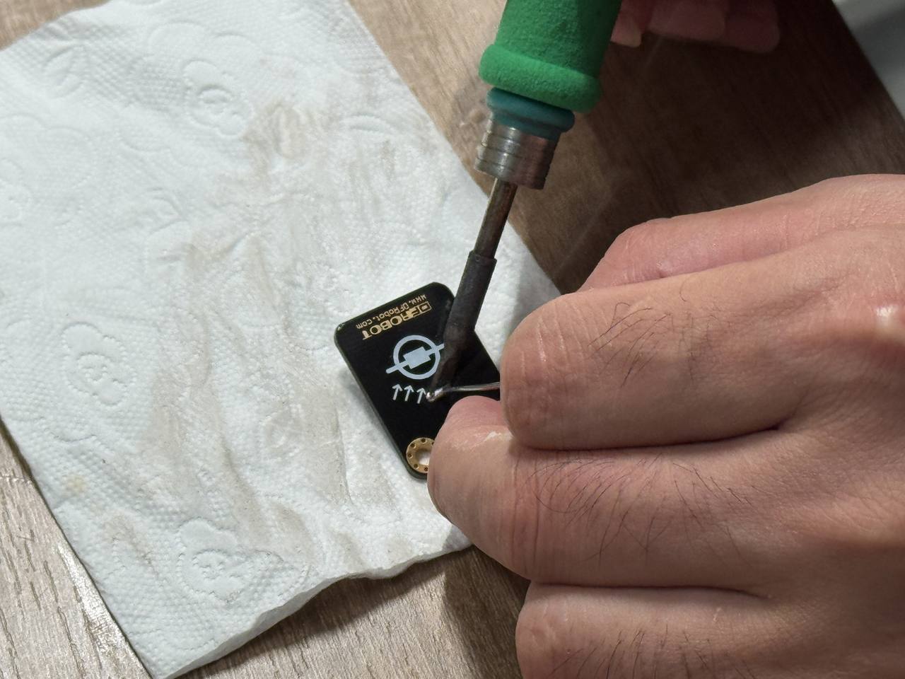
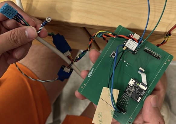
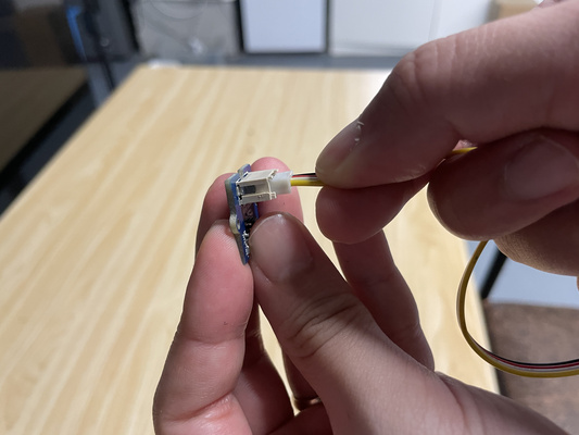
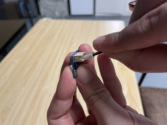
Soldering the light sensor and bring-out
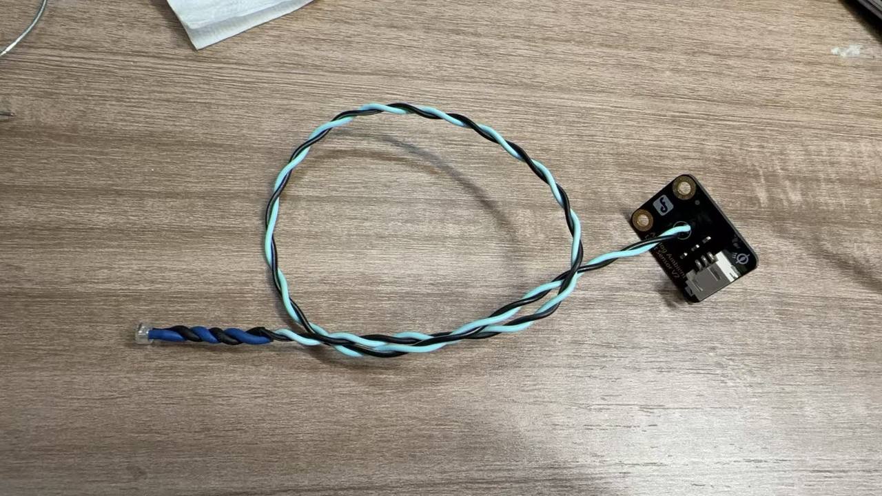
I hand-soldered the light sensor legs to the copper I routed for the divider, checked continuity with a meter, then added the rainbow bundle so the sensor head can live off-board in the final mechanical layout.
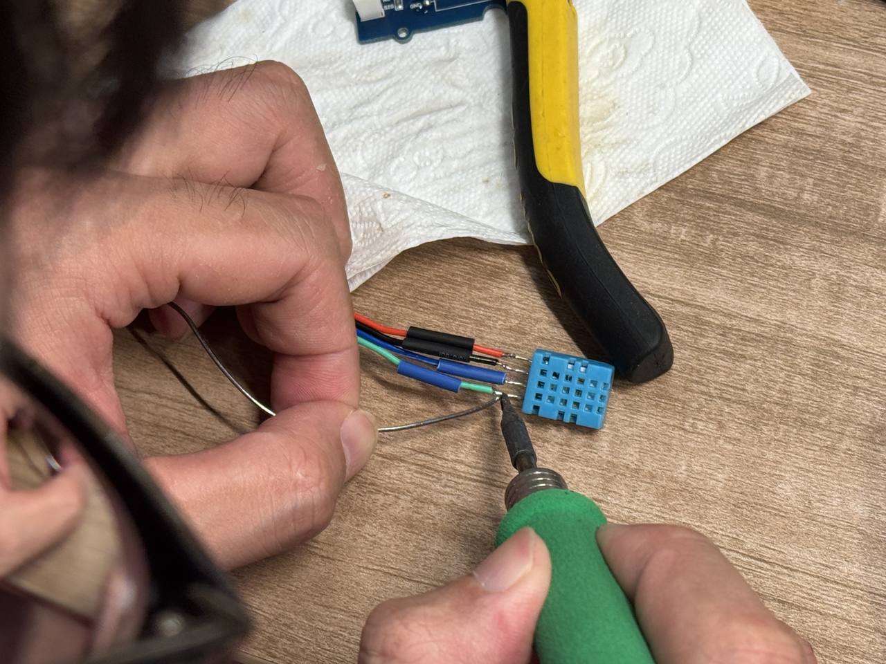
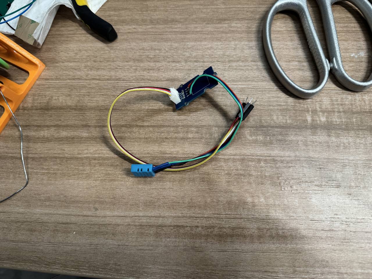
Soldering the DHT11 and bring-out
The DHT11 got the same treatment: anchor on the PCB, long leads for placement flexibility. I labelled the ribbon ends in my notebook so I would not swap data and power during final assembly.
Firmware and pin map
Week 9 evidence starts with serial print on the XIAO hub. I trimmed
the sensor loop from my S3上传程序 bench tree so the assignment sketch focuses on
input reading first; the full upload then packages the same values and sends them by I²C
to the WROOM UI. The file I treat as canonical for this week is
code/week09-s3-serial-env.ino,
which matches the hub print format used by the integrated firmware's
sampleSensorsAndPush() block. I also kept the earlier
code/week09-xiao-light-dht.ino
bring-up sketch because it shows the simpler one-line log and the Arduino
D2/D3 aliases from the first harness test. The full final-project
source is linked for traceability:
final-project-upload/s3-upload/src/main.cpp
reads DHT11 / light and packs TelemetryPacked with
i2c_env_link.h;
env_i2c_slave.cpp
and wroom-upload/src/main.cpp
receive and draw the environment packet; and
pico-upload/src/main.cpp
is the later Pico / NanoStat input source that prints STAT,... lines for the
S3 bridge.
| Signal | XIAO silkscreen | GPIO | Type |
|---|---|---|---|
| DHT11 data | D2 | GPIO3 | Single-wire digital |
| Light level (divider tap) | D3 | GPIO4 | Analog read → % of full scale (12-bit ADC) |
Every ~2.5 s the hub reads dht.readHumidity() /
readTemperature(), analogRead() on the light pin, and prints a
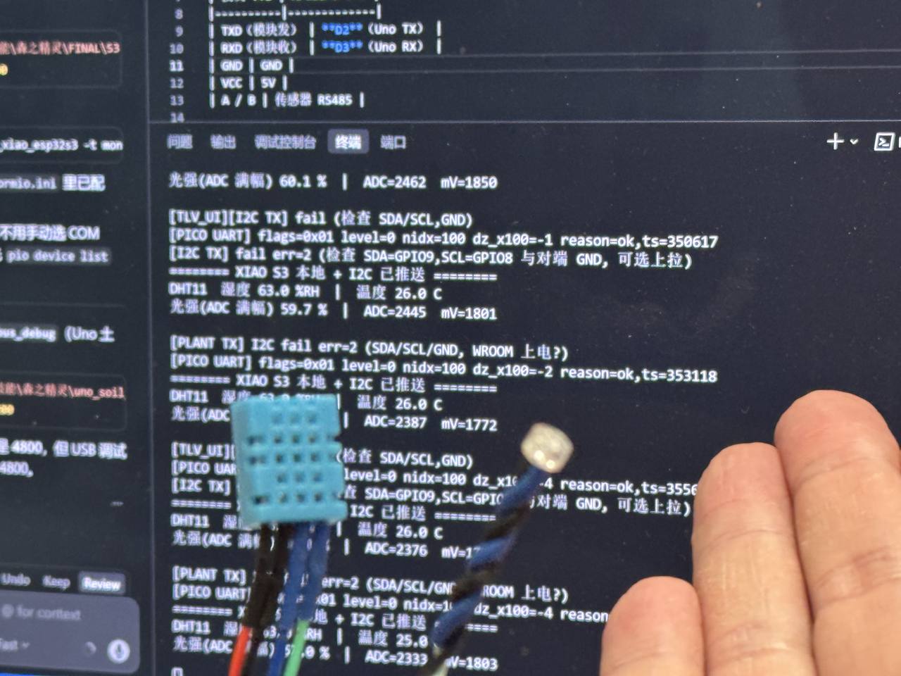
banner block at 115200 8N1 (USB CDC on the XIAO S3). Example:
======== XIAO S3 本地传感 ========
DHT11  湿度 45.0 %RH  |  温度 23.5 C
光强(ADC 满幅) 12.3 %  |  ADC=504  mV=405
NaN from the DHT usually means a loose data wire or a timing glitch: I re-seat D2 before blaming library code.
How the final-upload program reads and moves the data
In the full S3上传程序, the same read loop runs inside
sampleSensorsAndPush(). It samples humidity and temperature, checks
!isnan(), reads analogRead(kPinLight), converts the ADC count to a
percentage, and then calls pushTelemetry(). That function stores the values in
an 8-byte TelemetryPacked frame: magic byte 0xA5, command
0x01, DHT-ok flag, rounded RH percent, temperature multiplied by 10, and light
percent multiplied by 10. The S3 then writes the frame to the WROOM over I²C address
0x55.
On the WROOM side, env_i2c_slave.cpp receives bytes in an I²C interrupt,
pushes them into a ring buffer, and lets the main loop parse complete frames. It rejects
impossible values such as RH above 100% or light above 1000 tenths of a percent, updates an
EnvFromS3 snapshot, and increments a data-version counter so the UI redraws
only when the sensor data actually changes.
MCU reads sensors successfully
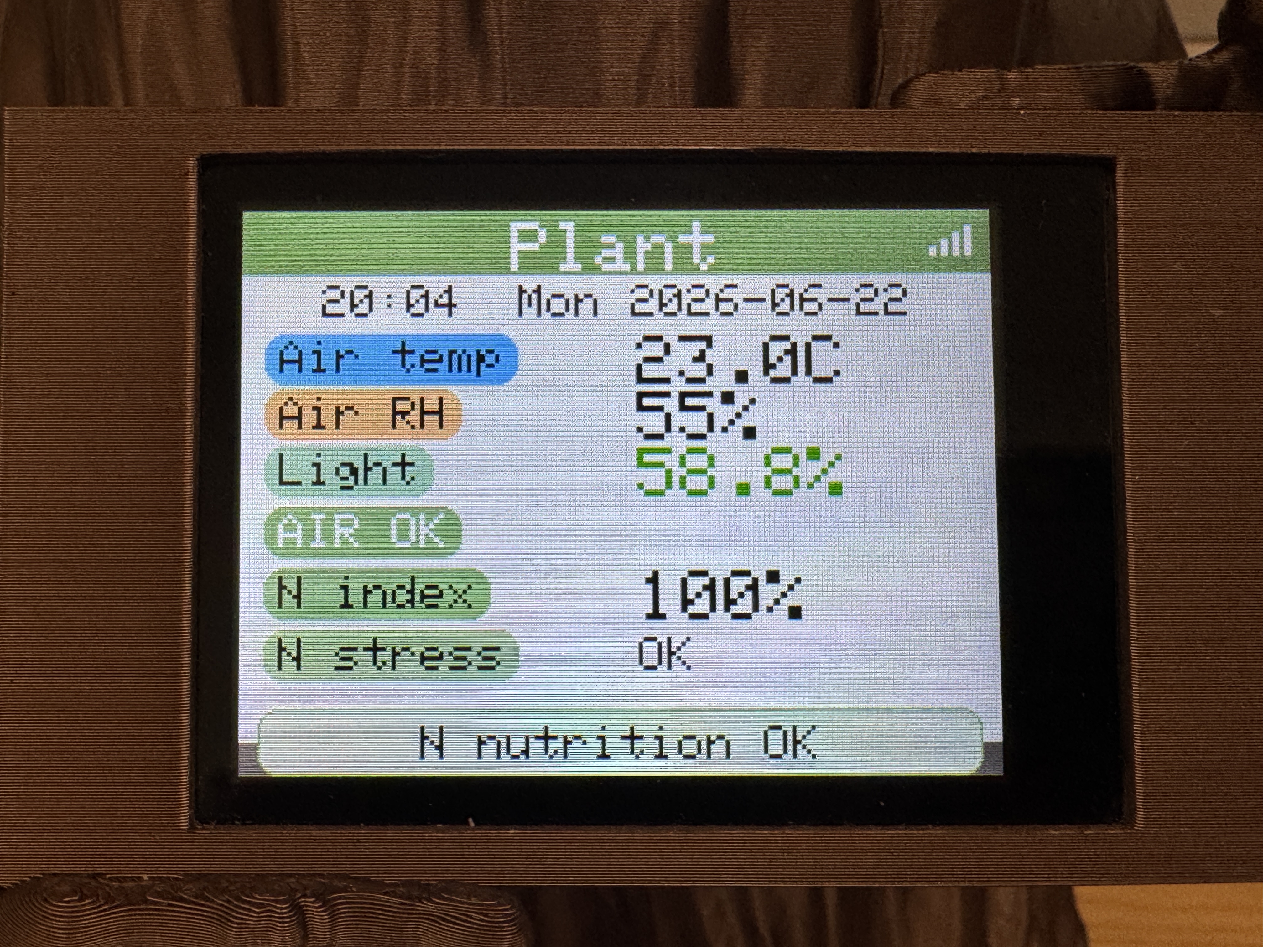
Displaying the same signals on a UI
Serial is enough for grading logic, but I also wanted a face-level check while moving the sensor heads around. I ran I²C from the XIAO on the PCB to a small OLED module on a breadboard (only the display stayed on headers; sensors and MCU are on copper). The screen shows humidity, temperature, and light percentage together.
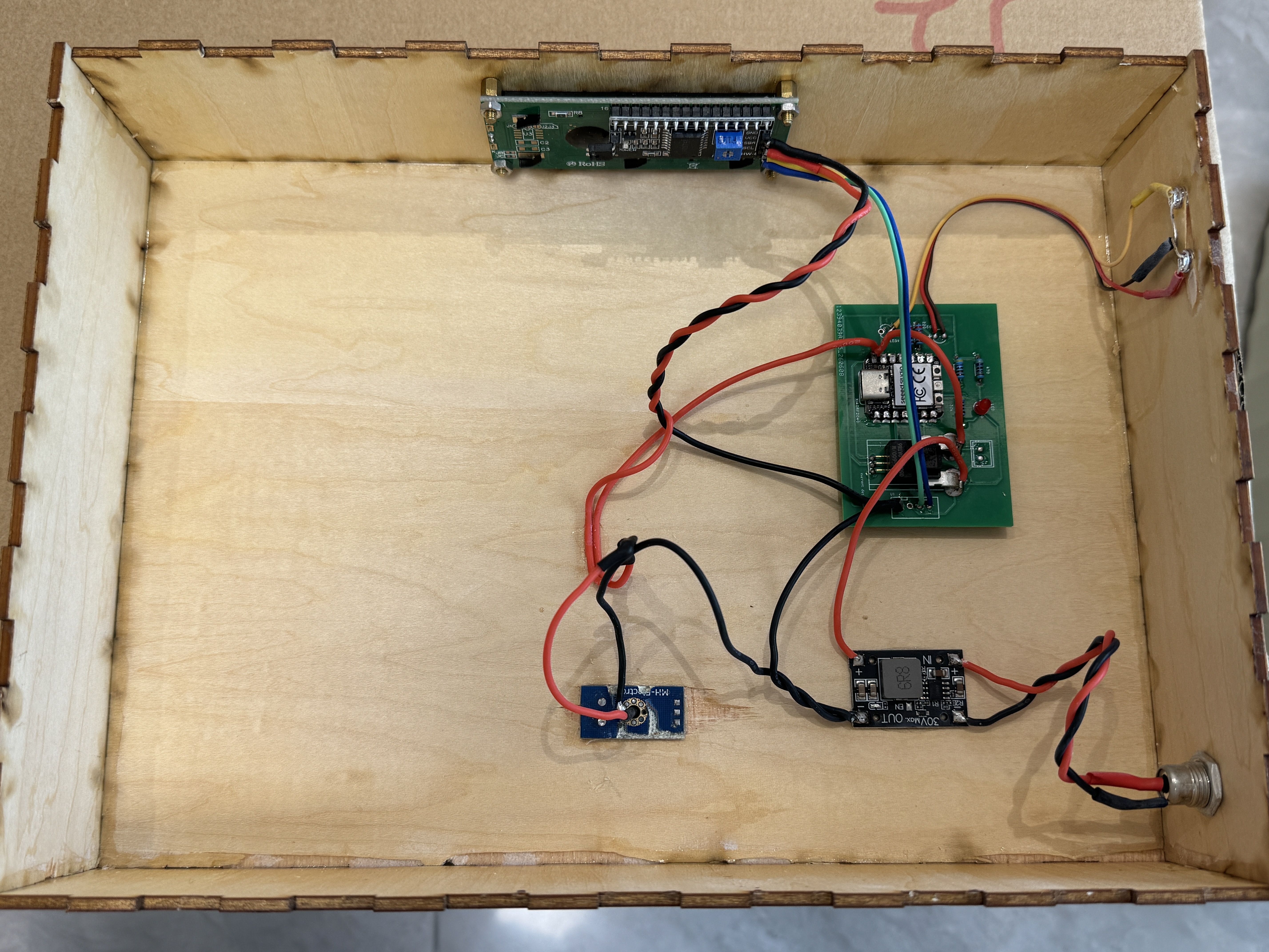
Charging dock: current sensor + voltage divider readout
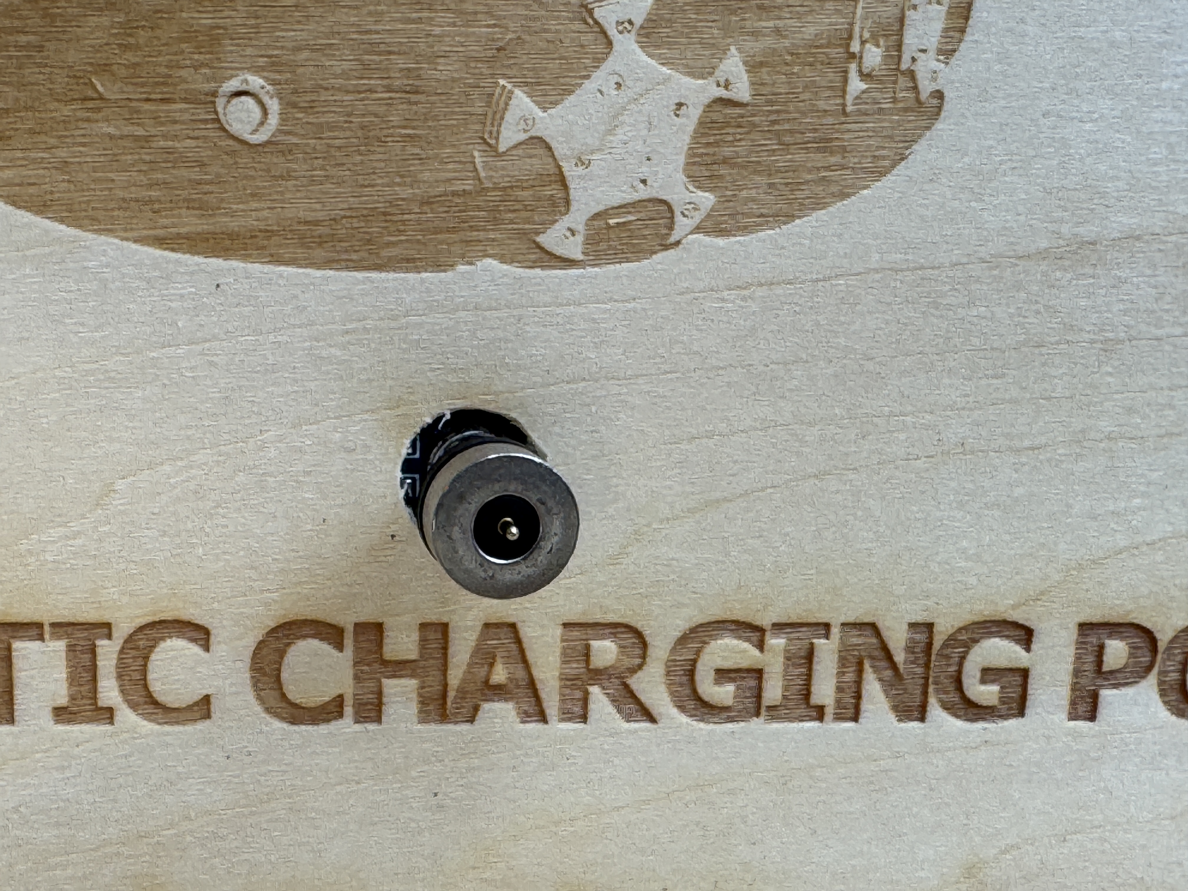
The dock is the second Week 9 input-device story. I wanted the enclosure to report how much current the robot draws and what voltage is on the charge port before I trust the magnetic contacts in the final assembly. The PCB was designed in Week 6 and fabricated in Week 8 ( charging-dock panel); this week I stuffed it, bolted on the Hall module, and checked that the ADC math matched a meter on the pogo outputs.
Source tree:
code/final-project-upload/charging_dock/src/main.cpp
(PlatformIO /
platformio.ini).
Below is the Week 9 core: average ADC reads, apply the divider and Hall formulas, then
print on serial once per second.
| Signal | XIAO pin | GPIO | Conversion |
|---|---|---|---|
| Charge voltage (divider tap) | A3 | GPIO29 | V = Vadc × 2 |
| Charge current (Hall module out) | A2 | GPIO28 | I = (Vadc − 2.514) / 0.028 (field-calibrated) |
static float readAdcVoltage(uint8_t pin) {
  uint32_t sum = 0;
  for (int i = 0; i < 16; ++i) {
    sum += analogRead(pin);
    delayMicroseconds(200);
  }
  return (sum / 16.0f / 4095.0f) * 3.3f;
}

static float computeVoltageV(float adcVA3) {
  return adcVA3 * 2.0f;   // 1:2 divider on the charge rail
}

static float computeCurrentA(float adcVA2) {
  return (adcVA2 - 2.514f) / 0.028f;   // Hall zero + V/A slope
}

// loop(): every 1 s @ 115200
Serial.print(F("[SAMPLE] Vadc=")); Serial.print(adcVA3, 3);
Serial.print(F(" V="));           Serial.print(voltageV, 2);
Serial.print(F(" Iadc="));         Serial.print(adcVA2, 3);
Serial.print(F(" I="));            Serial.print(displayCurrentA, 3);
Serial.print(F(" P="));           Serial.print(powerW, 2);
Serial.print(F(" dur_ms="));       Serial.println(g_chargeDurationMs);
After flashing, I opened the USB serial monitor at 115200 and checked that voltage tracked the divider (A3 × 2) and current moved when I loaded the charge port. The sketch also drives a 1602 LCD and status LEDs, but the graded input-device evidence here is the ADC path and the serial lines below.
Vadc, Iadc) beside
converted V and I so I can re-calibrate Vzero
and sensitivity without re-flashing blind.
Problems I hit
The first failure was DHT11 NaN after I lengthened the wires. The one-wire
protocol is sensitive to edge timing, so I re-soldered the data pin and kept that conductor
shorter than the power pair; most failures disappeared after that. The light reading had a
different weakness: because the divider references 3.3 V, USB sag appears as a few
percent of drift, so for this week I logged both raw ADC and percent instead of pretending it
was a calibrated lux meter. I also had to stop blaming libraries too quickly. A couple of
mistakes were just PIN_DHT / PIN_LIGHT not matching the silkscreen
row I had soldered. On the dock, the Hall module resting voltage was not exactly the datasheet
midpoint. I logged Iadc at no load, updated kCurrentZeroV in
charging_dock,
and re-checked that serial I stayed near 0 A until I drew real load current.
5. Conclusion
I used Cursor to code the assignment sketches in
week09-s3-serial-env.ino and
week09-xiao-light-dht.ino, plus the charging-dock ADC
loop in charging_dock/src/main.cpp.
I still calibrated kCurrentZeroV from live serial readings and checked DHT timing on the hub before
treating either path as done.
I can measure ambient light and RH/temperature on the Week 8 sensor hub, and charge voltage/current on the dock PCB, with both input interfaces on fabricated copper instead of a breadboard shim. The hub panel still has a NanoStat landing zone, but I left it empty this week. The rainbow harnesses on the hub are for the final mechanical layout; the dock Hall module and divider are fixed on the board I designed.
Next steps for input sensing: tuck the light and DHT heads into the plant enclosure and keep
this read loop. Next steps for the same PCB: mount and wire the NanoStat in
a later week when I merge plant impedance with the hub firmware (e.g.
week15 … s3-hub).
Design files: KiCad project: Week 6 electronics design; fabricated panels: Week 8 electronics production. Source: week09-s3-serial-env.ino (trimmed assignment sketch); week09-xiao-light-dht.ino (early); original final-upload files: S3 hub, WROOM I²C receiver, WROOM UI, Pico/NanoStat input; charging dock ADC + serial. Group reflection: group assignment on this page (scope / LA practice).
Group assignment (Chaihuo Makerspace)
The Fab brief asked us to probe input-device analog levels and digital waveforms with a multimeter, oscilloscope, and logic analyzer, and write down what we saw, not to polish a product. Our cohort reused the Seeed Grove ecosystem on the input side and treated every screenshot as lab notebook evidence.
A fuller regional write-up with the same structure lives on the Fab Academy site: Week 9, Group Assignment: Input Devices (Fab26 Chaihuo). What follows here is our mirror: English notes and media we actually captured in the room.
How we thought about input devices
We kept reminding ourselves that sensors translate physics into voltage or timed bits. Analog inputs, such as a wiper or LDR divider, often look like steady DC when the thing being measured moves slowly, but they still carry noise and settling behaviour worth measuring. Digital inputs can be single wires with switch bounce, quadrature pairs, or framed packets. That is why the scope and logic analyzer answer different questions: one shows shape, the other helps decode meaning.
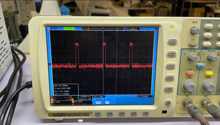
Lab gear we used
We used the DT-660B digital multimeter for rails, continuity, and slow sensor DC while someone moved a knob. The OWON EDS102 CV oscilloscope gave us two analog channels at 100 MHz / 1 GSa/s, and we avoided autoset so the volts/div, time-base, coupling, and trigger choices stayed visible to us. For protocol work we used the Alientek DL16 logic analyzer; its sixteen channels and ≥50 MSa/ch buffer captures were enough for the UART and I²C decoding we needed.
The rule we repeated before each measurement was: tie scope/LA ground to circuit ground before touching signal probes. A floating ground gave us nonsense traces once, so we checked ground before moving the signal probe on the next measurements.
Devices we characterised together
| Device | Principle | Signal type | Instrument |
|---|---|---|---|
| Grove rotary angle sensor | Potentiometer | Analog DC (slow) | DMM + scope |
| Grove button | Mechanical contact | Single-ended digital | Scope |
| Grove rotary encoder | Quadrature switches | Two square waves | Scope (CH1+CH2) |
| Grove RTC (DS1307) | I²C clock IC | I²C | Logic analyzer |
| Grove I²C OLED (SSD1306) | Display updates | I²C traffic reference | Logic analyzer |
| Grove GPS (Air530) | NMEA UART | Serial @9600 8N1 | Logic analyzer + host capture |
Grove four-pin harness sanity check
Grove cables bundle GND, VCC, SIG1, SIG2. When we used loose jumpers, we caught one power/signal swap before powering the board. A quick visual check saved us from debugging a problem we would have created ourselves.
Scope baseline workflow we repeated every bench session
At the start of each scope session we used Utility → Factory Setting → confirm to clear old settings from the previous user. For single-channel captures we hid CH2, then turned it back on when the rotary encoder needed quadrature. CH1 stayed on DC coupling, with time-base adjusted so one to three cycles, or one slow ramp, filled the screen without clipping vertically. The trigger sat inside the signal swing, around 2.5 V for a 0–3.3 V logic-like waveform, because otherwise a healthy signal looked unstable. When the probe corners looked dull or rang badly on the front-panel square-wave calibrator, we trimmed the probe compensation before measuring the real circuit. The Measure soft keys gave frequency, VPP, and duty readouts, which kept us from estimating every value by counting divisions.
Analog: rotary angle sensor
The Grove module is a 10 kΩ pot wired rail-to-rail with the wiper exposed. At 3.3 V we measured about 0.00 V → 3.28 V from end to end with the handheld meter. The voltage changed smoothly, so the track did not look damaged.
On the scope we slowed time-base (~500 mV/div vertical, ~200 ms/div horizontal) so knob rotations drew ramps rather than pops. Result: essentially DC plus tens-of-millivolt ripple when the knob was still. That is small enough for this class exercise, and the transitions were smooth enough that heavy firmware filtering was not necessary.
Analog: faster-changing waveform sanity capture
We also chased an analog output whose voltage visibly danced inside one sweep window so we could practise triggering slightly above idle — resting traces jitter otherwise even when hardware behaved.
Digital: button on a pulled-up GPIO
We moved the probe to the microcontroller pin (XIAO ESP32-C3, internal pull-up enabled) so we measured the same node firmware samples. Idle sat around 3.3 V, presses pulled it low, and mechanical bounce showed as rapid chatter before settling — textbook reason we debounce in software or with RC networks.
The idle-high rail picked up tiny USB ripple yet stayed confidently above CMOS recognized-high threshold; documenting ripple is more useful than pretending rails are flat.
Digital: rotary encoder quadrature
Two square waves ~90° apart: whichever channel edges first spells direction. Each detent produced one clean A/B cycle — exactly what interrupt-driven decoders expect.
Protocol: I²C (RTC + OLED reference)
DS1307 at address 0x68 shared the bus with an SSD1306 OLED we already
trusted. The XIAO master polled once per second; logic analyzer inputs were
D0→SCL, D1→SDA with decoder set to I²C.
Clean captures showed clocks bursting ~100 kHz, data toggling only while SCL low per spec, decoder listing address byte, R/W, register pointer, seven time-bytes with ACKs. OLED-heavy segments stretched transactions dramatically — instant illustration why bus capacitance and pull-ups matter: long loose wires without pull-ups rounded edges until decoders threw framing errors; restoring 4.7 kΩ-ish pull-ups at 3.3 V put teeth back on edges.
Protocol: UART GPS (Air530 @9600 baud)
TX idles high, the start bit goes low, eight data bits arrive LSB-first, and the stop bit releases high:
classic 10-bit ASCII frames. Indoors we still saw text streaming even when fixes were
garbage (empty fields / zeros); outdoors $GPRMC / $GPGGA
sentences filled with real coordinates once the antenna saw sky.
We measured the narrowest pulse width at about 104 µs as a baud-rate sanity check. Its inverse is about 9600 baud, which is useful when a UART module is not labelled.
What stuck with us
Match the instrument to the question: scopes for waveform shape, logic analyzers for packet meaning. Ground first; our “broken probe afternoon” traced to floating grounds or swapped Grove legs. Trigger inside the swing, or jitter starts to look like bad hardware. I²C without pull-ups rounds edges until decoders report bad frames. We wrote volts/div, time/div, and trigger level beside each screen capture so we could retrace the setup later.