Week 6: Electronics design
Electronics design week. I compared EDA tools, chose KiCad, and ran the schematic → PCB flow for a carrier around Seeed XIAO RP2040: FPC and pin-header breakouts toward a display, a tactile switch with pull-up, an indicator LED with series resistor, plus decoupling and routing. The steps below are what I actually clicked through so someone else could repeat the workflow; screenshots cover the schematic and PCB editor. After the first fab order I spun a second PCB revision (smaller FPC, 1×6 header, ESP32-S3 for Nanostat programming/UART). See Revision 2 below.
Individual assignment: KiCad dev board
How I approached the week
I compared a few EDA options and stayed on KiCad because I want to own Gerbers and keep the project in Git without a paid seat. The long section below is deliberately step-by-step. ERC, net labels, and “update PCB from schematic” were where I got stuck until I treated the schematic as logic only and the board as the only physical truth. If anything in your build differs (panel connector pinout, pull-up value), swap the numbers but keep the same discipline: verify pins against the datasheet before you order.
Each step states the goal, what to click in KiCad, and why it matters for a board that actually powers up.
I used KiCad 7 (menus are similar in 8.x). If you replicate the circuit, verify pin numbers, voltage, and
your display’s flex pinout against the datasheet. Labels like WE/RE/CE
here are temporary net names for a memory-style interface and must match your panel.
How this board meets the assignment
My map from Fab “electronics design” expectations to what is on the sheet and the PCB:
| Requirement | This design |
|---|---|
| Controller | Seeed XIAO RP2040 with a DIP-style symbol/footprint for hand-soldering and breadboard-friendly bring-up. |
| Input |
Tactile switch (SW1) on GPIO with a
pull-up (R1): released = logic high,
pressed = tied to GND. You can reuse the same pattern for
BOOTSEL or reset-style lines if you route them on a
variant board. Always define idle state with a resistor so the pin never
floats.
|
| Output |
FPC (J1) toward a flex display, plus an
on-sheet LED (D1 + R2) for a
simple “firmware alive” indicator while bring-up debugging.
|
| Connectivity |
No on-board wireless; USB through the XIAO module for
power and serial. Optional 2×8 header (J2)
parallels the same display-related nets for probes, jumpers, or a
breakout.
|
| Fab stock / Fab library | I chose passives and connectors that match lab inventory and footprints in the Fab / course KiCad libraries (0603/0805, headers, FPC land patterns). Match package, pitch, and voltage rating to the BOM before you order or stuff the board. |
Step 1: Choose EDA and create a KiCad project
I compared three common options: KiCad (free, open-source, cross-platform), Eagle (Autodesk / Fusion ecosystem), and Altium Designer (commercial, common in industry). For Fab Academy style work (small runs, owning your own Gerbers, sharing projects on Git), KiCad is the most straightforward default.
The KiCad mental model took me a while to get right. The schematic is only the logical design: symbols, nets, and ERC rules. It is not copper yet. Every symbol still needs a matching footprint, because the footprint is the land pattern I will actually solder. After that, the PCB editor is where the physical decisions happen: placement, tracks, pours, clearances, and DRC. Once I understood that split, the workflow became less mysterious. I created a new KiCad project, checked the symbol and footprint libraries, added the XIAO / Fab library tables from the lab, opened the schematic editor, and saved the sheet before placing anything. From then on, every schematic change had to be pushed with Update PCB from Schematic, otherwise the board and the logic quietly drift apart.
Step 2: Draw the schematic (symbols, nets, power)
The sheet centers on Seeed XIAO RP2040 (U1), a
tactile switch with pull-up, an LED branch, and
connectors toward the display bus (FPC J1 and
2×8 header J2). Below is the order I actually clicked
through in the schematic editor; each screenshot matches one step.
2a. Place components
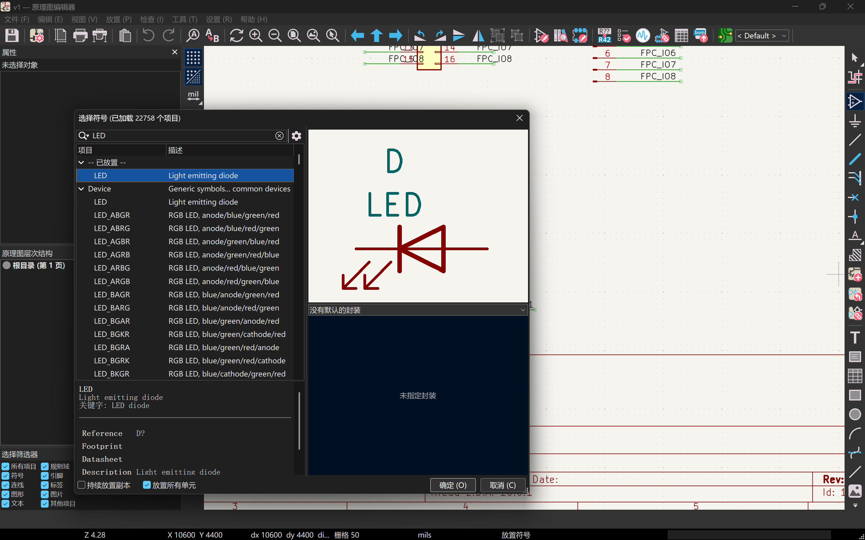
In the schematic editor, click the third icon in the right toolbar (Add symbol), search the library, and place parts on the sheet. The capture uses an LED as the example, but the same flow applies to the XIAO module, switch, resistors, and connectors.
2b. Place power symbols
Click the fourth icon in the right toolbar to add
power symbols (GND, +3V3, and so on).
Every supply pin needs a deliberate return path; I place both rails before I start
wiring signal nets.
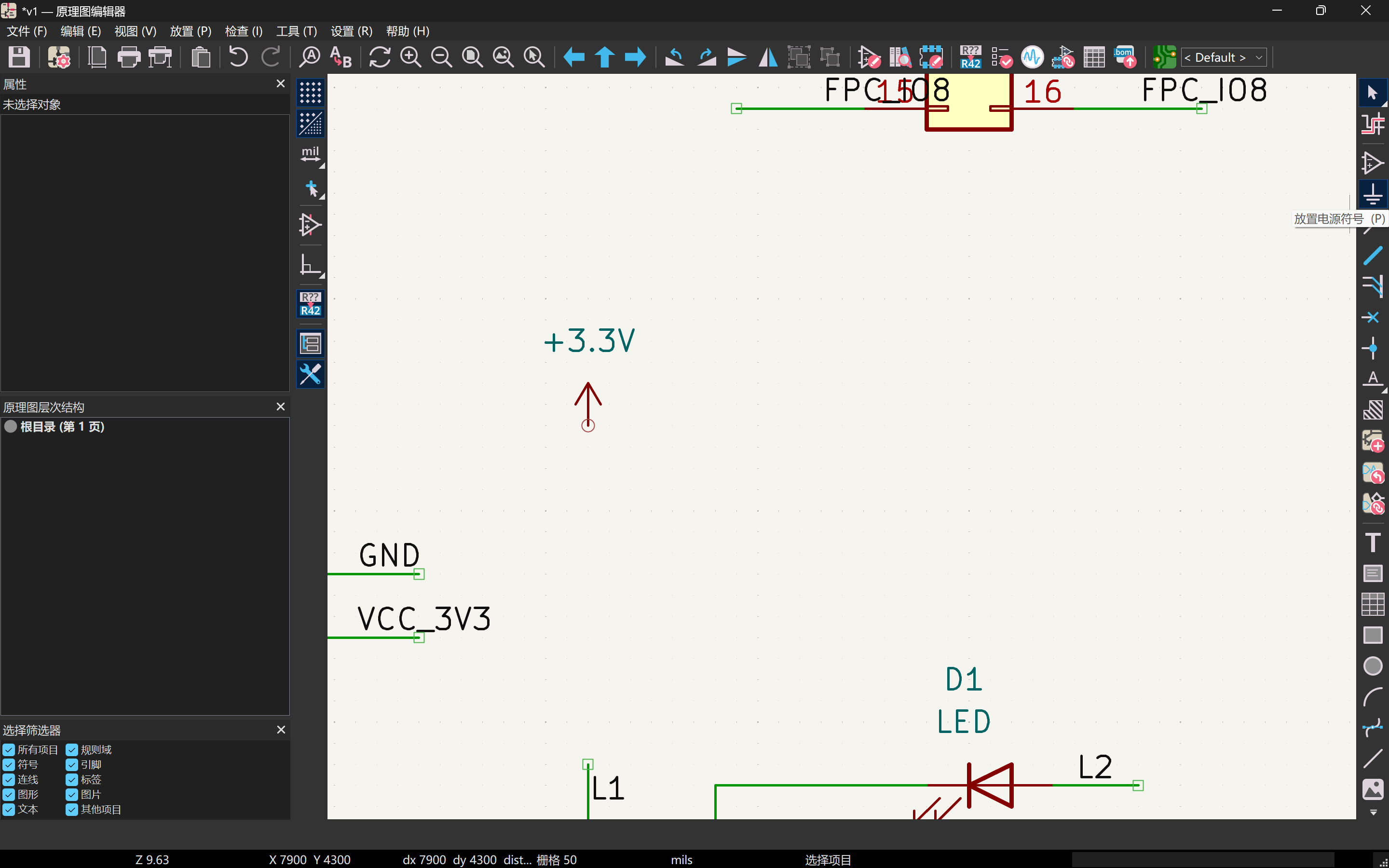
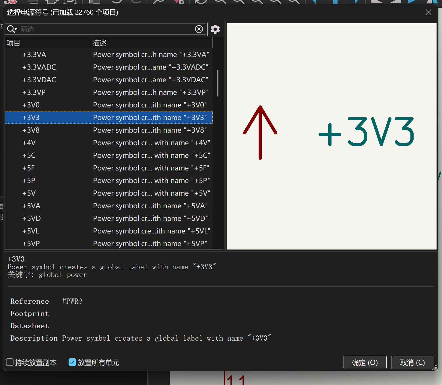
2c. Select the 3V3 symbol
From the power-symbol chooser, pick +3V3 (or the label your sheet
uses, such as VCC_3V3). Place one instance near each block that needs
logic supply; duplicate with C once the first copy is on the sheet.
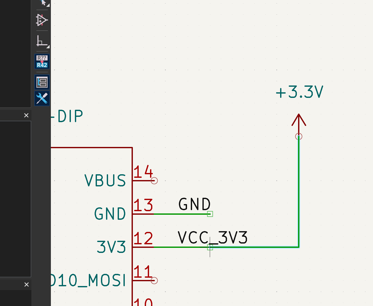
2d. Connect 3V3
Wire each +3V3 symbol to the matching supply pins on
U1 and to pull-ups (for example R1 on the switch net).
Use the wire tool or click pin-to-pin; same net name ties distant nodes together
when you add net labels later.
2e. Wire signals and mark unused pins
Finish the signal paths: switch + pull-up on L1, LED + series resistor
on L2, display nets on J1/J2. For MCU or
connector pins that stay unused, place a no-connect flag (the
small X) so ERC does not treat them as floating inputs.
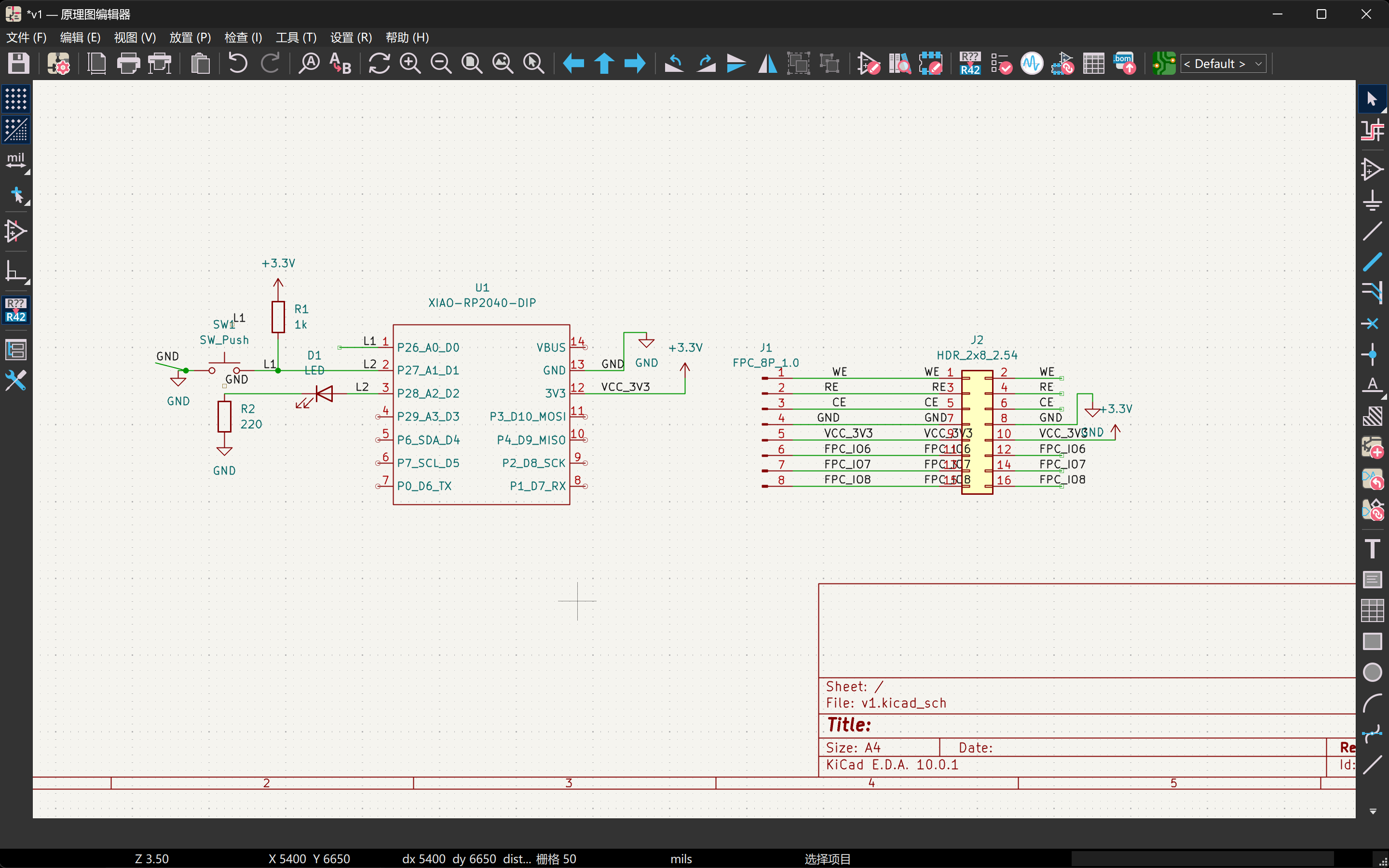
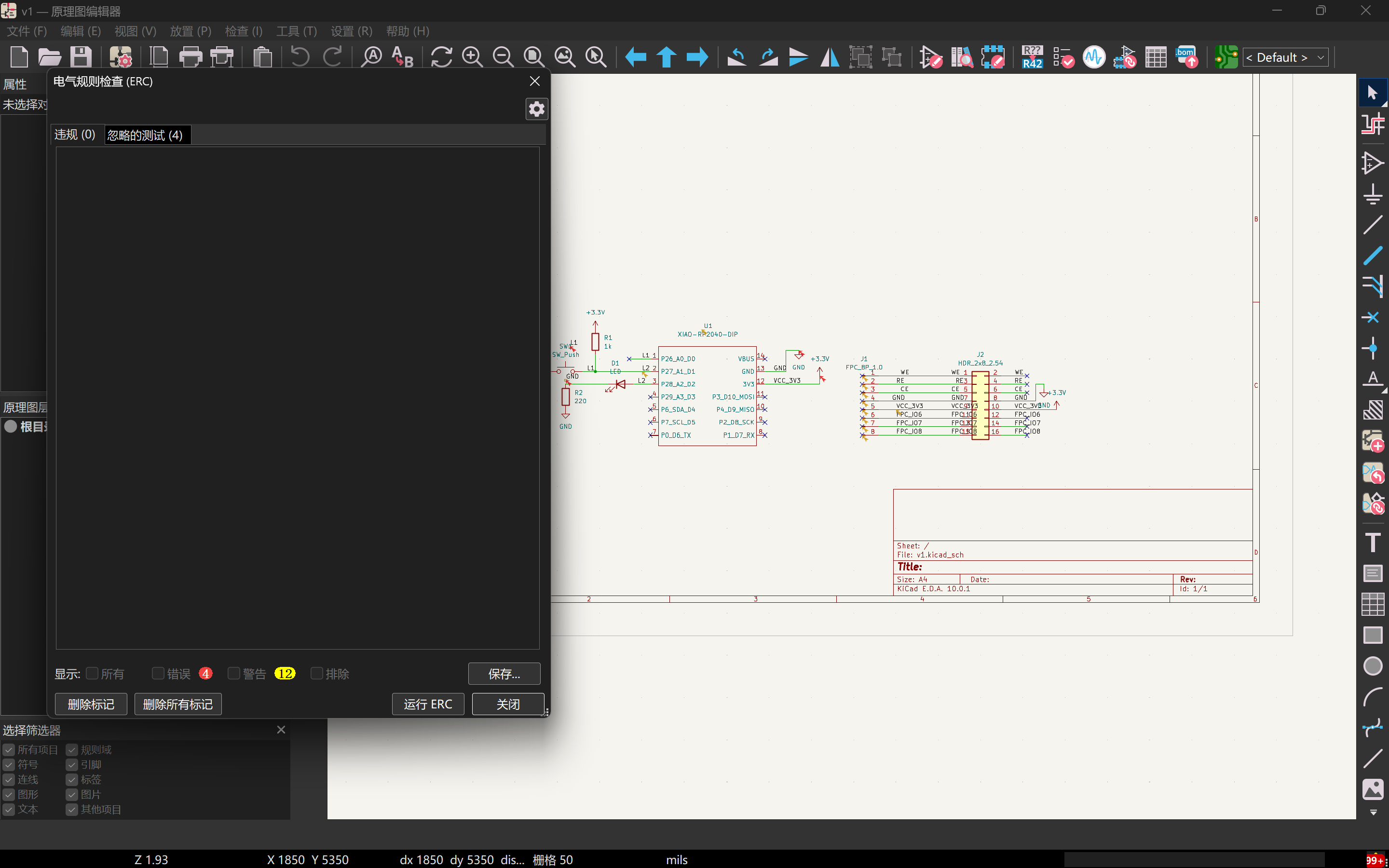
2f. Run ERC
Run Inspect → Electrical Rules Checker. Fix errors (missing
GND, floating inputs, power pins not driven) before syncing to PCB.
The capture below is the pass I kept before moving on to footprints.
Step 3: Footprints and “Update PCB from Schematic”
For each symbol, assign a footprint that matches the part you will solder:
passives as 0603/0805/etc., SW_Push to the exact switch from the
drawer, J1 to the FPC’s vendor land pattern (or a verified KiCad
footprint with the same pitch and stagger). Then:
- Tools → Assign Footprints… Work left-to-right: filter library, pick footprint, apply. Missing footprints mean DRC cannot be trusted yet.
- Open the PCB Editor. Run Tools → Update PCB from Schematic… Accept initial placement (everything may stack in a pile; that is normal).
-
Set File → Board Setup…: board thickness if known, minimum
track/space compatible with Fab milling or your PCB vendor’s 6/6 or 8/8 mil
class rules, via sizes, and netclass widths for power if you widen
3V3.
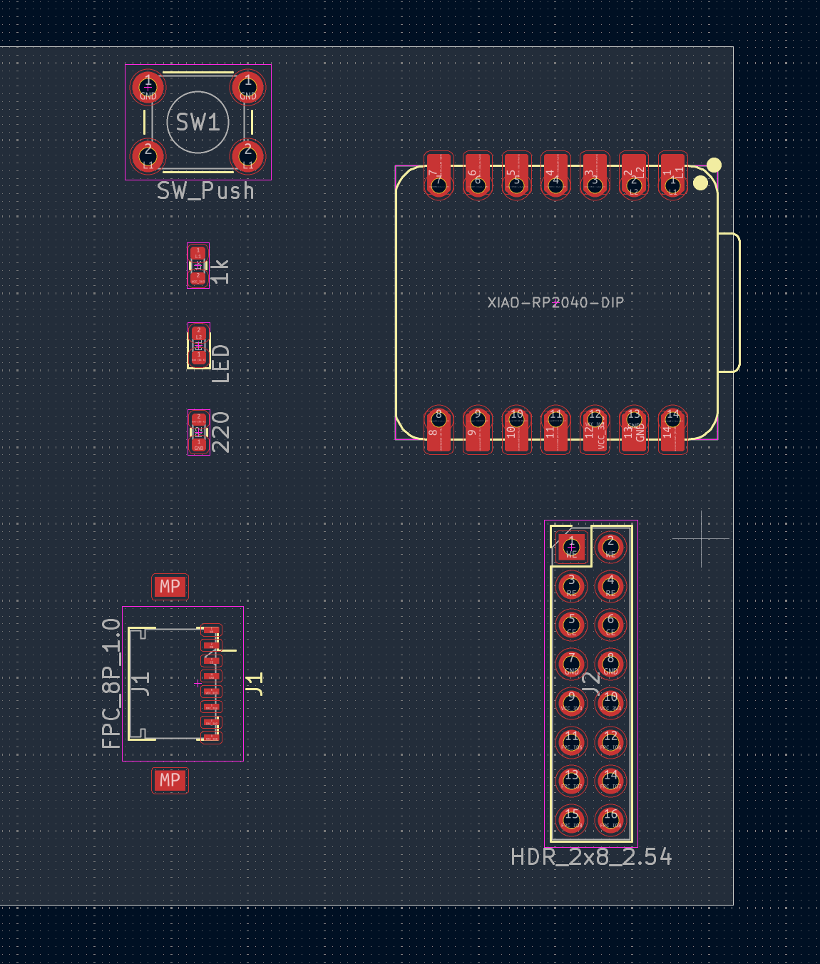
Step 4: Placement: outline, connectors, bypass caps
Before routing, I dragged the footprints out of KiCad's first messy pile and treated
placement as a mechanical problem. The XIAO had to sit with its USB edge exposed at
the board edge, with keepout for the connector shell. The FPC had to
sit on the side where the flex cable can bend naturally, and I checked pin 1
against the silkscreen before locking the orientation. I moved the switch to an edge
I could actually reach after assembly. The small decoupling capacitors on
3V3 and GND stayed close to the module pins, with short,
direct routes instead of decorative placement halfway across the board.
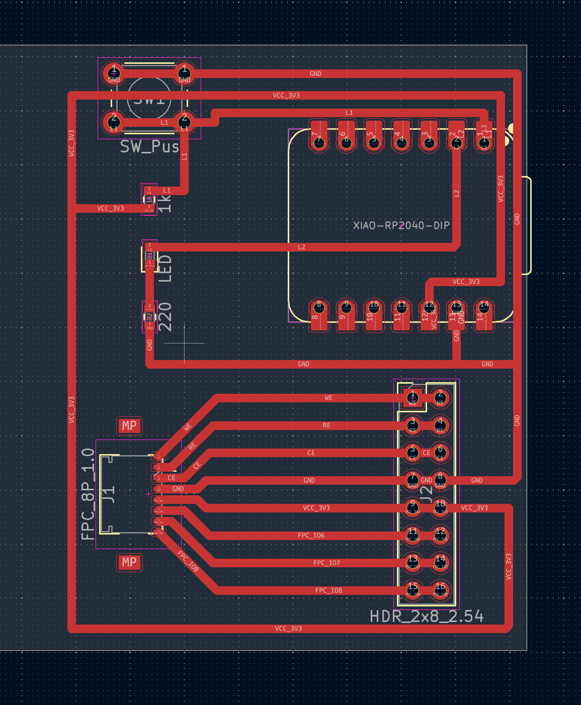
Step 5: Route copper, pours, and run DRC
I routed in the order that caused the least trouble: display / bus lines and
switch-style nets first, then GND pours, then cleanup around escapes
and vias. For the FPC breakout, I kept lanes organized and avoided
broken ground under return paths; I did not force equal length because this interface
did not require it. The switch net stayed short and close to its ground return instead
of wandering near noisy edges. After each meaningful routing pass I re-ran
DRC, fixed clearance and drill complaints, and only moved on when the
remaining warnings had a reason I could explain.
This layout is the direction I want for my final project carrier: RP2040 XIAO for software support, flat flex to the display, and a switch pattern I can reuse for configuration lines in firmware.
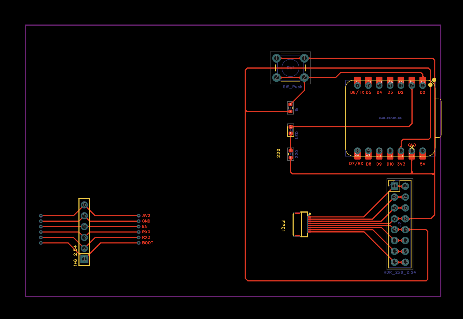
Revision 2: connectors, Nanostat flashing, ESP32-S3
After I had already paid for and received the first PCB batch (about CNY 100), laying the real board next to the rest of my system made a few mismatches obvious, so I went back into KiCad for a second spin rather than cutting up the old outline and adding jumper wires everywhere.
In revision 2 I replaced the original display FPC with a smaller FPC footprint that matches the flex connector I actually want on the mechanical stack, and I added a 1×6 pin header right beside that area so those signals are easy to break out, useful for probing, dongles, or short harnesses during bring-up without only relying on the flex.
For the final project I plan to dock a Nanostat board that brings out six pads dedicated to flashing / field updates; among them, two pads are UART (serial) and must reach the main MCU. Earlier iterations were drawn around XIAO RP2040; this revision moves the design to Seeed XIAO ESP32-S3 so those two UART lines from the Nanostat interface can tie straight into the ESP32-S3 for download and serial logging, while the six-pad footprint still carries the wider programming pattern the Nanostat expects. The schematic steps in Step 2 still reflect the RP2040 sheet I practiced on before the layout spin; mentally swap the MCU block for ESP32-S3 when you map GPIO names and USB/UART straps to this board revision.
Design files (download)
KiCad sources for this week’s board (revision 1, XIAO RP2040 carrier).
Open both in KiCad 7/8: schematic first, then the matching PCB. If the browser shows plain
text instead of saving, use Save As… or right-click →
Download linked file so the extension stays
.kicad_sch / .kicad_pcb.
Figures on this page live under images/week06/…; design sources under
design-files/week06/….
Group assignment
Guangzhou (Chaihuo) group documentation: using lab test equipment to observe an embedded microcontroller board.
Abstract
In the lab, the group used a digital multimeter and a digital storage oscilloscope to measure voltage and observe signals on a running embedded board (custom purple PCB with ESP32-WROOM, OLED, pushbuttons, and LEDs, USB-powered). Dial positions, wiring, and instrument readings were recorded to meet the Week 6 group assignment: use lab test equipment to observe the operation of an embedded microcontroller.
Location: Chaihuo Makerspace
Instruments: Digital multimeter DT-860B; digital storage
oscilloscope OWON EDS102CV
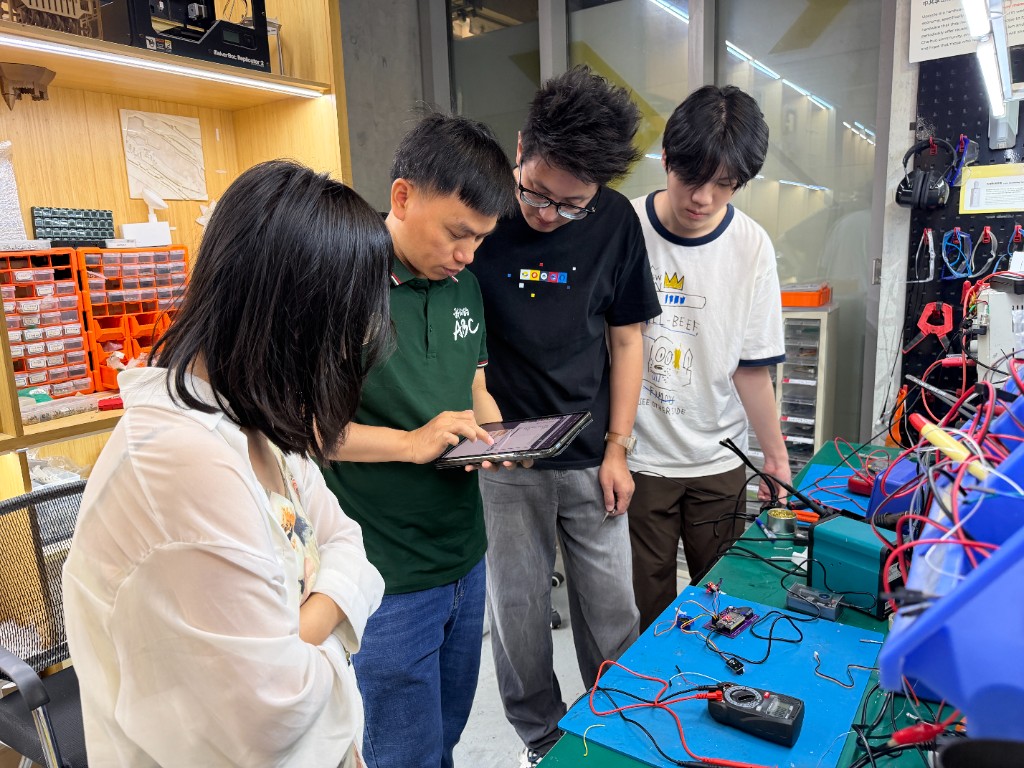
1. Teamwork and lab setup
Before measurements, the group reviewed wiring and the measurement plan at the bench and checked steps against reference material on a tablet.
Using the meter and scope at the bench forced me to slow down and tie each reading back to what the firmware was doing on the purple PCB, not just write down a number.
Breadboard / dev-board wiring was completed in the same space; the multimeter, jumper wires, and microcontroller board were visible on the table for shared work.
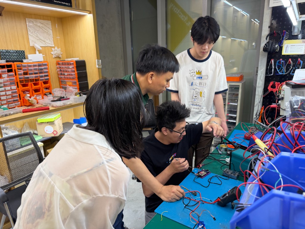
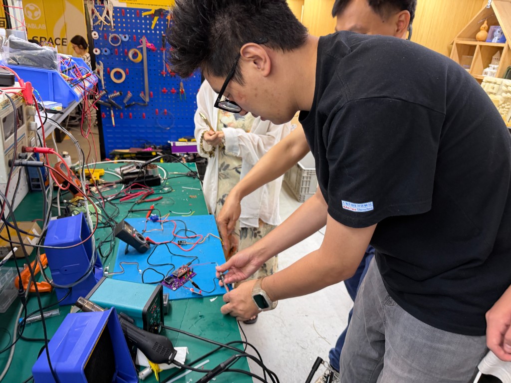
At the Chaihuo Makerspace station, members soldered or probed the purple PCB using an iron or probes together with test gear; the multimeter, soldering station, and bench power equipment were arranged on the bench.
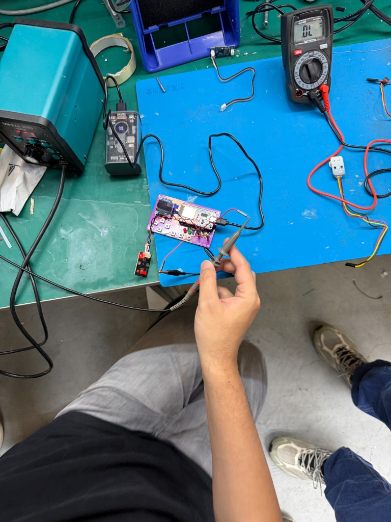
2. Device under test
| Item | Description |
|---|---|
| Main board | Custom purple PCB with on-board ESP32-WROOM module |
| HMI | Small OLED display, several tactile pushbuttons, multiple LED indicators |
| Power | USB cable to the board edge (debug / power); a portable power module was also used on the bench (see oscilloscope setup photos) |
| Peripherals | Small red sensor daughterboard on a multi-wire harness (red / black / white, etc.); on-board and peripheral LEDs could be lit during tests to confirm operation |
All measurements below were taken with the board powered and firmware running.
3. Multimeter
3.1 Model and range
We used a DT-860B multimeter on the DC voltage range, checking probe placement and range before touching the powered board. The black lead went to COM, and the red lead went to the VΩmA (μA) jack because we were measuring voltage, resistance, and low-current style checks only. The 10 A jack stayed unused in this session, which helped avoid the common mistake of putting the meter in the wrong current path.
3.2 DC voltage (parallel)
Set the dial to the DC voltage (DCV) range, 20 V scale (suitable for ~5 V logic / supply). Place the probes in parallel across the supply or load.
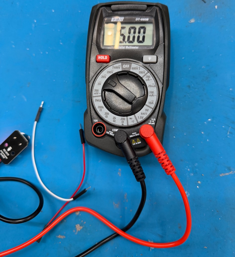
The reading was 5.00 V (interpreted per the selected voltage range), indicating a stable DC level at that node for comparison with oscilloscope high / low levels.
3.3 Probe short check (continuity / low-resistance)
Before measuring the circuit, touch the two probe tips together to confirm probes, leads, and meter inputs are OK; the display in the photo shows 001 (low-ohms / continuity-style indication per this meter and range).
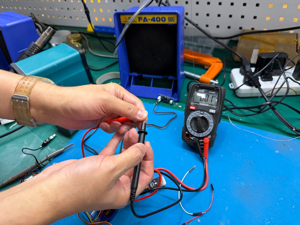
Safety: For current, break the path and connect the meter in series with the correct jack and range. For voltage, use parallel placement; do not short high-current paths. When in doubt, start on a higher range.
4. Oscilloscope
4.1 Model
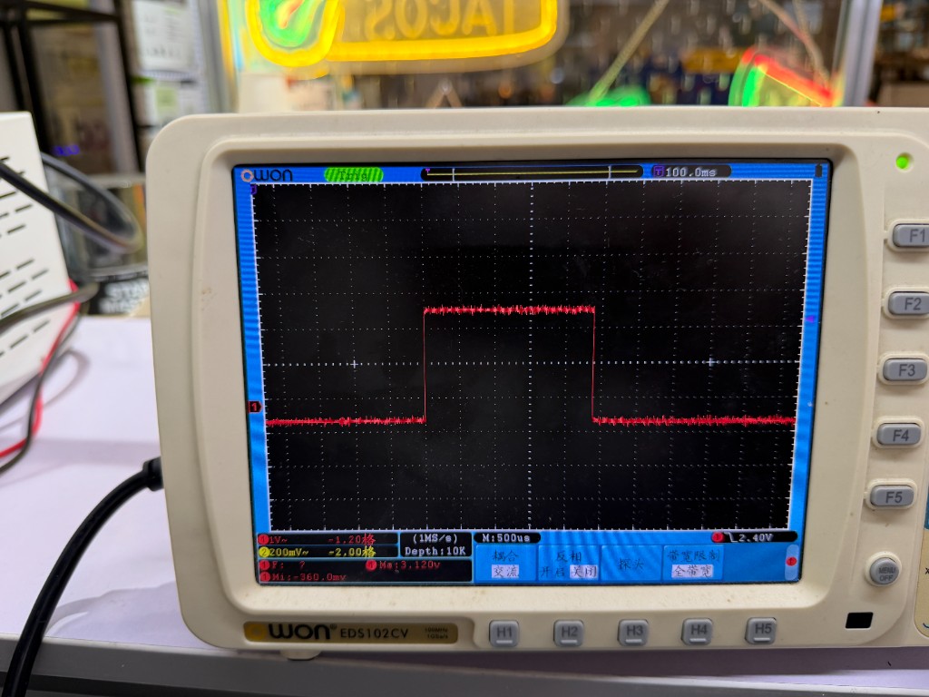
The scope for this session was an OWON EDS102CV digital storage oscilloscope.
4.2 Probe wiring
Clip the probe ground (alligator clip) firmly to circuit GND; touch the probe tip to the pin or test point. Keep the ground lead short to reduce ringing.
Overall setup (oscilloscope, DUT, USB power, and probe):
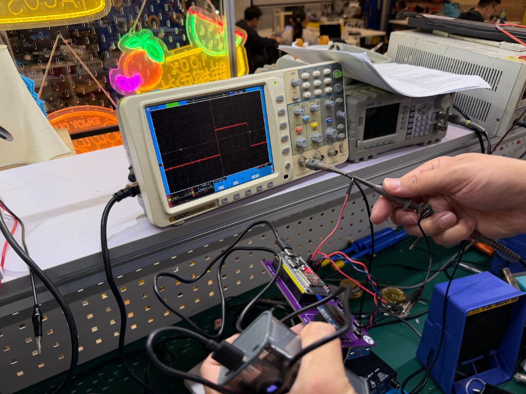
4.3 Waveform capture
Using the OWON EDS102CV, the group observed the signal on the selected pin, adjusted vertical and horizontal scales and trigger until the trace was stable, then captured the screen image below.
5. Bench supply and logic analyzer
The bench included a soldering station and DC power-related equipment. This report does not include separate bench supply panel readings. A logic analyzer was not used this week.