Week 15 — System Integration
Assignment
Design and document the system integration for your final project.
Here is my plan for the week.
What I Did This Week
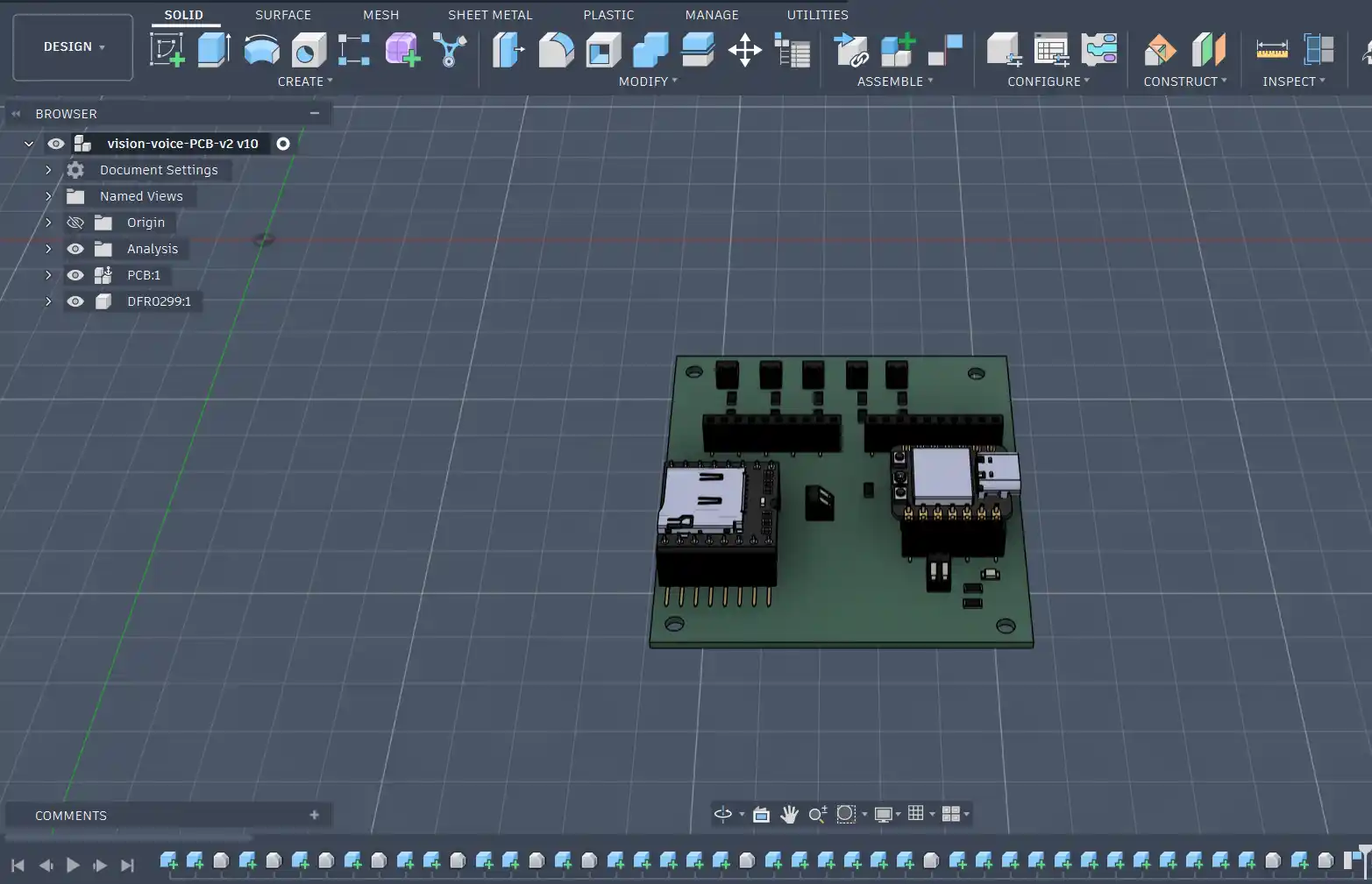
This week was all about bringing Vision Voice together as one actual system instead of a bunch of separate components. The main thing I did was design and mill the final Vision Voice PCB — the full board with every component considered. I also connected everything up and did a test run of the whole system. The ADS1115 modules haven't arrived yet so I did a short-wire workaround for now, but everything else — OLED, MPU6050, DFPlayer, speaker, button, LiPo — is running through the real PCB. It worked first try which honestly felt really good after all the component testing from the previous weeks. ^-^
The Vision Voice System Plan
Before I opened KiCad I wanted to be clear on how Vision Voice actually comes together as a complete system. The idea is that it is fully self-contained — no phone, no laptop, nothing external. Just the glove and the wrist casing.
The glove has 5 flex sensors, one on each finger. The wires from those sensors run down the back of the hand into a casing on the wrist. Inside the casing is the PCB which holds everything — the XIAO ESP32-C3 which is the brain, two ADS1115 ADC modules that read all 5 flex sensors over I2C, an MPU6050 IMU that reads the hand orientation, a DFPlayer Mini that plays audio from an SD card, an OLED display that shows the detected gesture as text, a button for calibration and playback, and a LiPo battery to power it all. The XIAO runs a kNN gesture recognition algorithm that takes the flex sensor readings and the orientation data together and figures out which ASL gesture is being made, then shows it on the OLED and plays the audio through the speaker.
Here is the full system block diagram showing how all the subsystems connect:

This diagram was generated by Claude AI. Click here to view the prompt.
Components
| Component | What it does |
|---|---|
| XIAO ESP32-C3 | Main microcontroller, runs the kNN model |
| ADS1115 x2 (0x48, 0x49) | Reads all 5 flex sensors over I2C |
| MPU6050 | Reads hand orientation (accel + gyro) |
| OLED SSD1306 0.96" | Shows detected gesture as text |
| DFPlayer Mini | Plays audio files from SD card |
| Flex sensors x5 | One per finger, detects bend angle |
| LiPo 3.7V | Powers everything |
| Push button | Short press for audio, long press to calibrate |
| Speaker | Audio output |
How Everything Talks to Each Other
| Bus | What's on it |
|---|---|
| I2C on D4/D5 | OLED 0x3C, MPU6050 0x68, ADS1115 #1 0x48, ADS1115 #2 0x49 |
| UART on D6/D7 | DFPlayer Mini |
| GPIO D1 | Button |
Planning the PCB with Claude AI
Before I touched KiCad I used Claude to plan out all the connections and figure out some things I wasn't sure about. I'm only covering the wiring and connection decisions here since that's what actually affected the PCB design.
Connector types for each component
I needed to figure out how each component physically attaches to the board. The OLED sits on the face of the wrist casing and the MPU6050 goes on the back of the hand — both need long flexible wires to reach, so I went with direct solder pads on the PCB for those instead of connectors. The ADS1115 modules, XIAO, and DFPlayer all go on SMD female pin headers so they can be removed if needed. Everything else — flex sensors, battery, speaker, button — uses screw terminals so the wires are easy to swap without soldering.
Finding the right resistor value
I wasn't sure what resistor values to use for the flex sensor voltage dividers so I ran a test first before committing to anything on the PCB. I used 10kΩ + 4.9kΩ SMD resistors and uploaded this quick sketch that Claude helped me write to check the range:
#define FLEX_PIN A0

int minVal = 4095;
int maxVal = 0;

void setup() {
  Serial.begin(115200);
  pinMode(FLEX_PIN, INPUT);
}

void loop() {
  int val = analogRead(FLEX_PIN);
  if (val < minVal) minVal = val;
  if (val > maxVal) maxVal = val;
  int range = maxVal - minVal;
  Serial.print("Current: "); Serial.print(val);
  Serial.print("  |  Min: "); Serial.print(minVal);
  Serial.print("  Max: "); Serial.print(maxVal);
  Serial.print("  |  Range: "); Serial.println(range);
  delay(100);
}
The range came out to around 1835 between fully open and fully closed which is really clean. So 10kΩ + 4.9kΩ is what went on the PCB.
Battery wiring
Since the XIAO sits on female pin headers the BAT pad underneath isn't reachable after it's mounted. The fix was to solder a wire directly to the BAT pad before mounting the XIAO, then run that wire to the LiPo screw terminal. The DFPlayer VCC also goes to that same terminal because it needs battery power directly and not the XIAO's 5V pin.
Button logic
I kept it to 1 button. Short press plays the audio, long press calibrates. No reason to add a second button when the logic already handles both.
Decoupling capacitors
I added 100nF ceramic capacitors on the VDD pins of both ADS1115 modules. The ADS1115 datasheet says these are needed because the chip draws transient current during conversion and without the cap it can make the analog readings unstable.
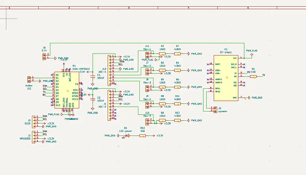
Step 1 — Schematic in KiCad
I started a new KiCad project called vision-voice-PCB-v2.
I opened the Schematic Editor and started adding all the component symbols from the library.
I dropped everything on the canvas first before wiring anything — XIAO, DFPlayer, both ADS1115 connectors, OLED and MPU6050 solder pad connectors, all the screw terminals, resistors, capacitors, and the power LED.
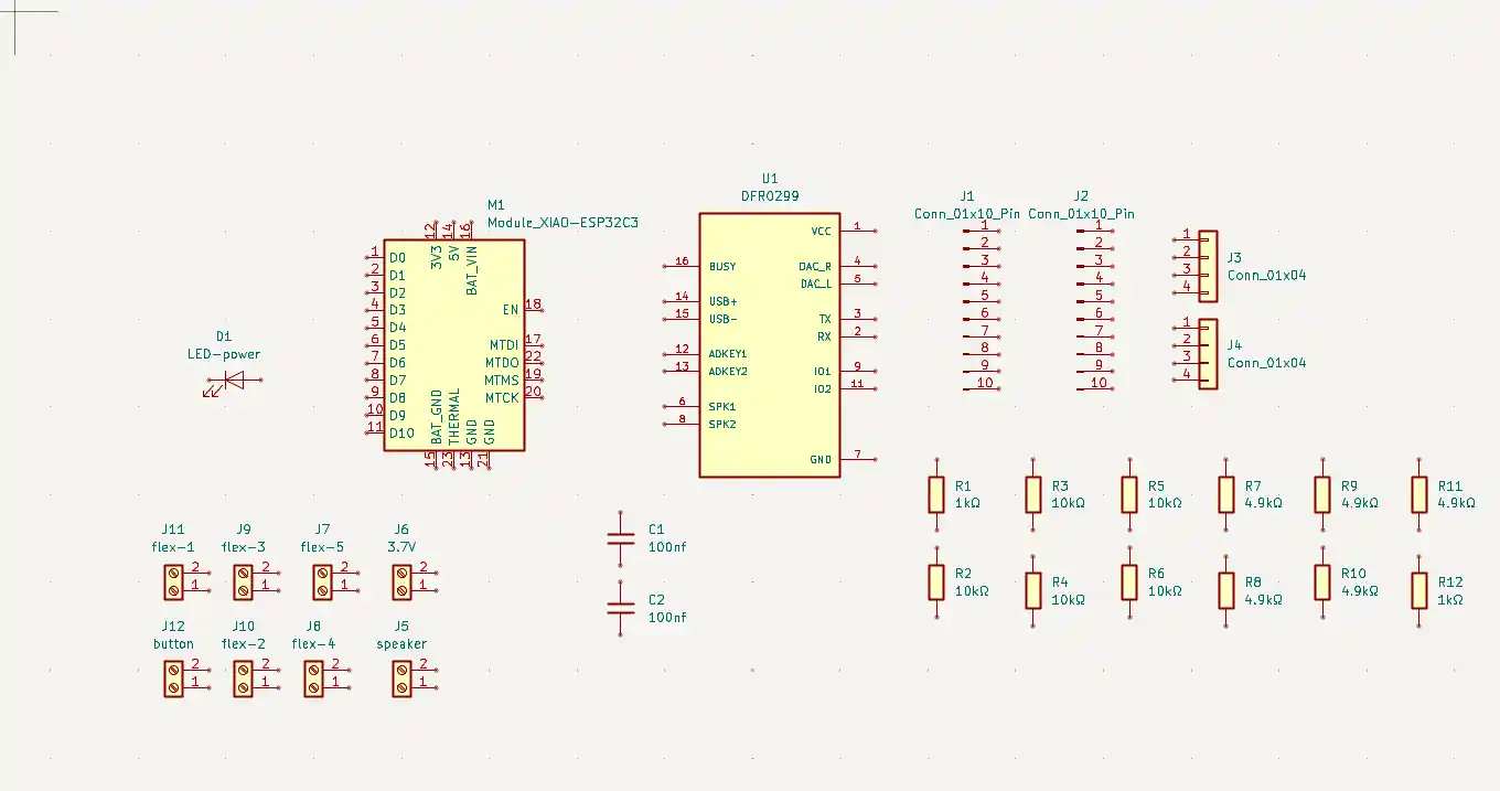
Then I started wiring. I used net labels for all the shared nets — SDA, SCL, 3.3V, GND, BAT_POS — so the schematic stays clean and readable instead of wires crossing everywhere.
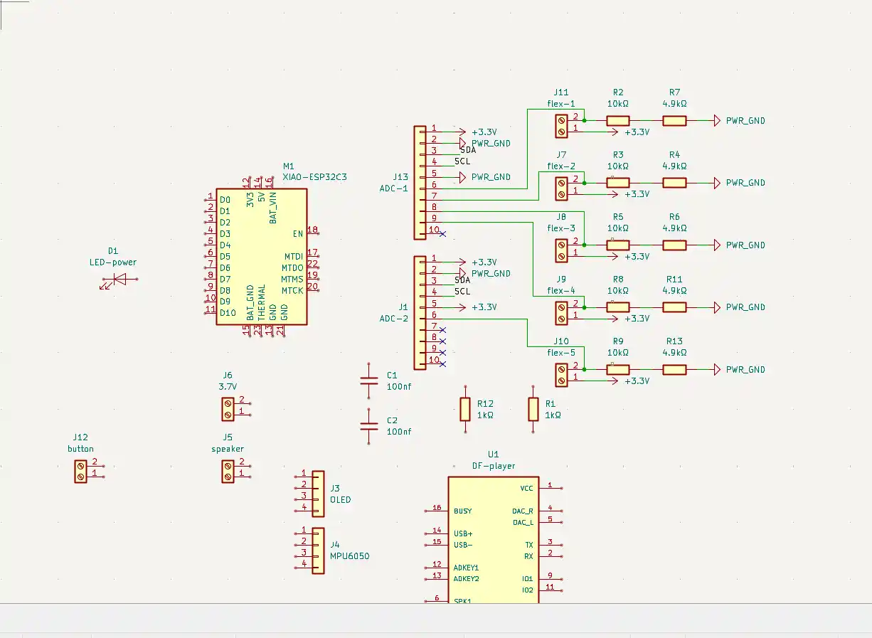
Here is the finished schematic with everything connected.
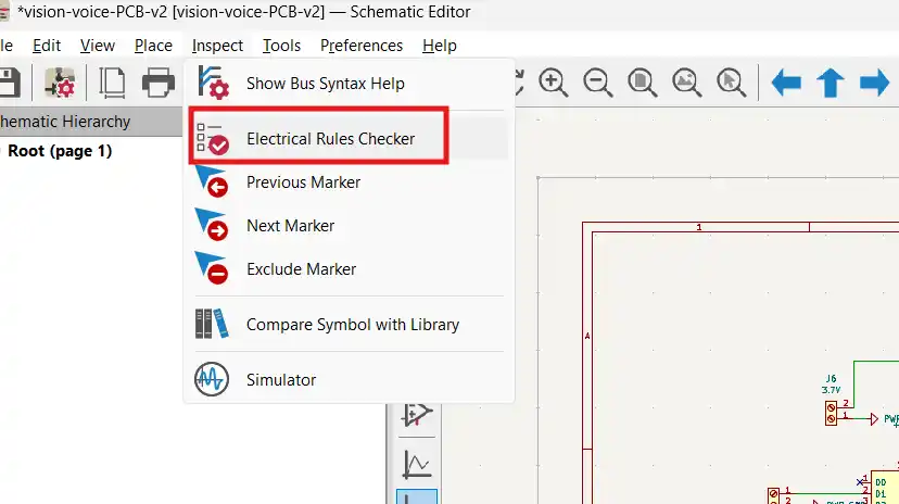
I ran the Electrical Rules Checker to catch any issues.
I had a couple of errors — missing PWR_FLAG symbols on the power nets and a dangling label. Fixed both and ran it again. Final result was 0 errors and 1 warning.
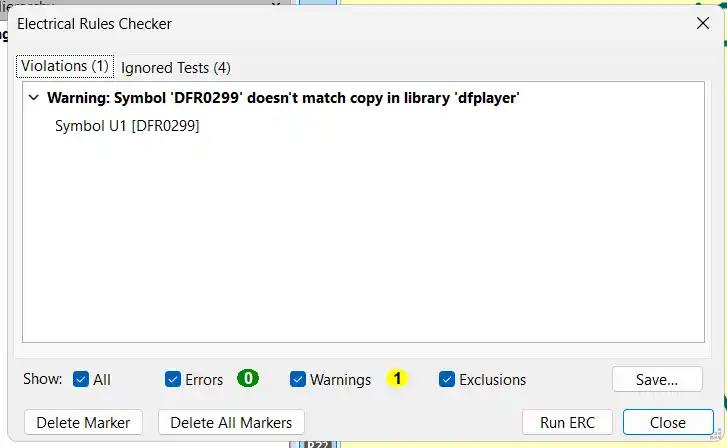
The warning is just a symbol mismatch on the DFPlayer because the symbol I downloaded is slightly different from the library version. It doesn't affect anything electrically so I left it.
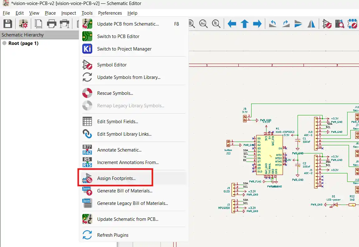
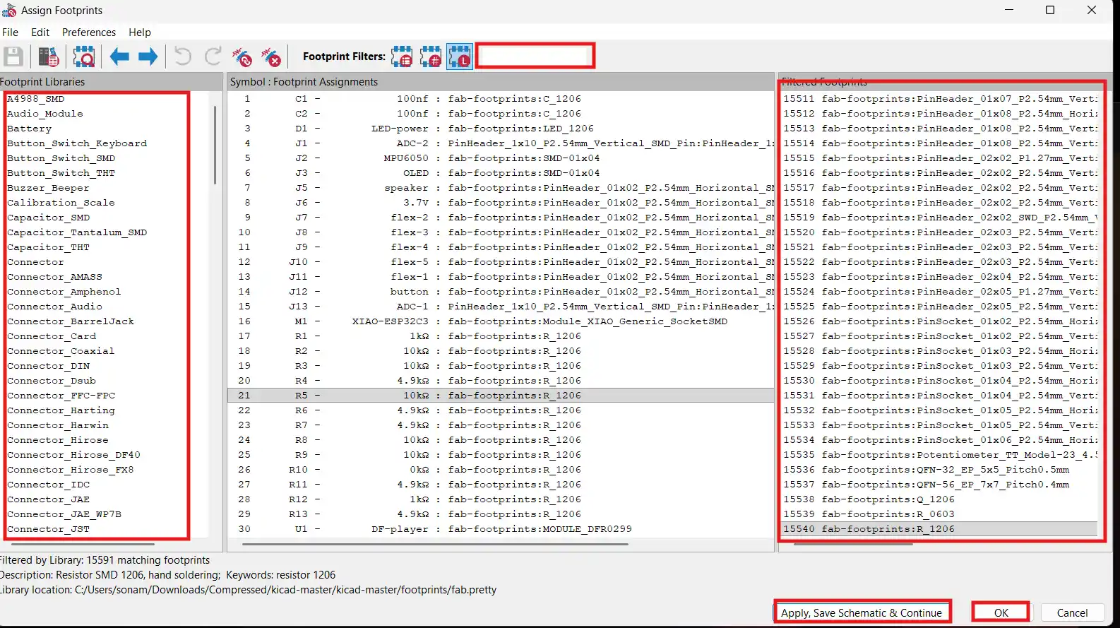
After the schematic I went to Tools → Assign Footprints and matched everything to the fab-footprints library.
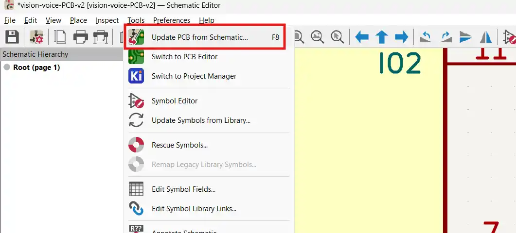
Then I pushed it to the PCB editor using Tools → Update PCB from Schematic.
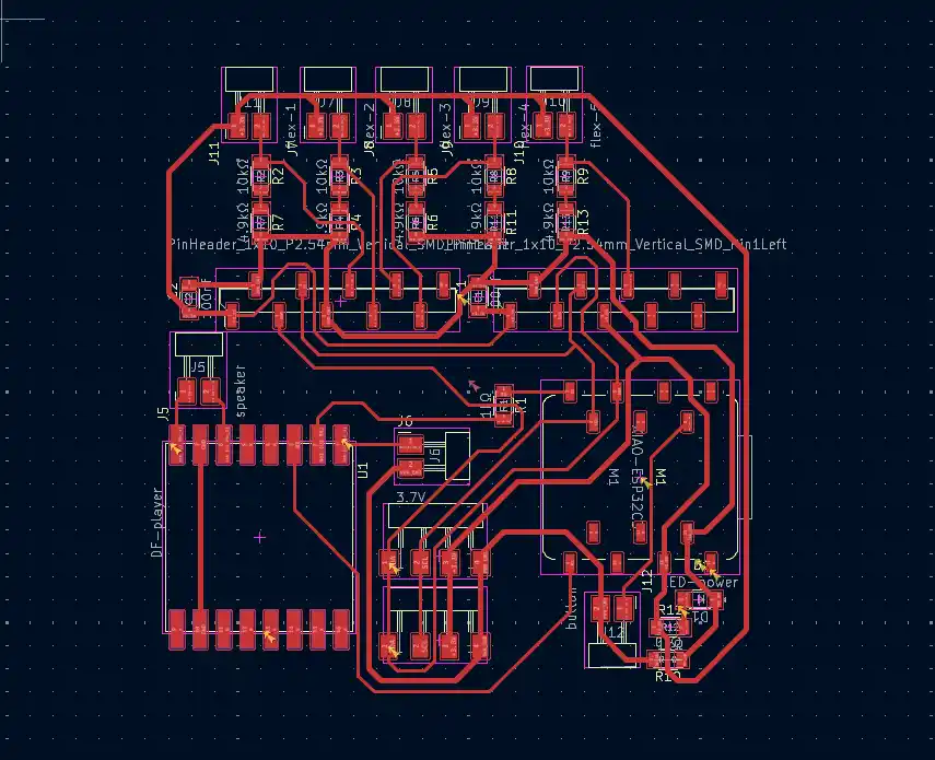
Step 2 — PCB Layout and Routing
All the footprints came into the PCB editor with 61 unrouted connections as ratsnest lines.
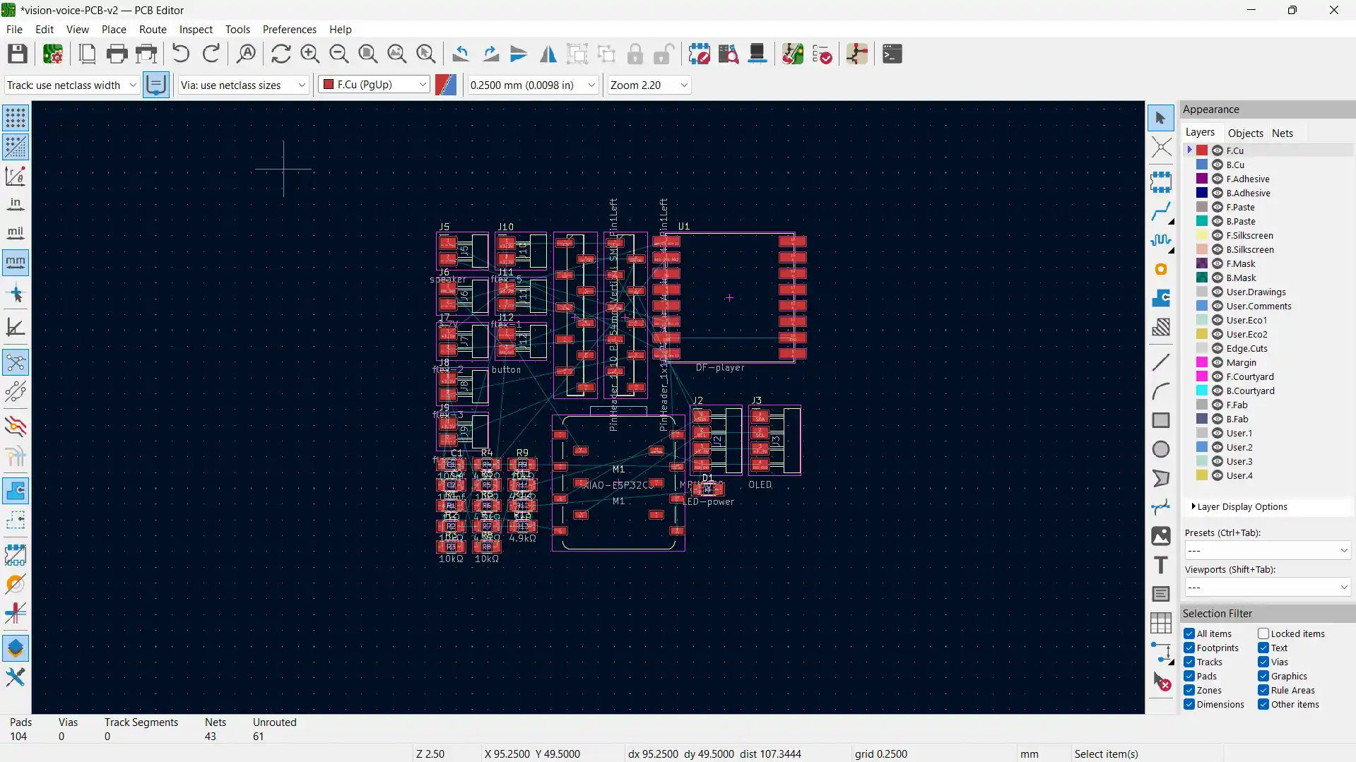
I placed everything thinking about how Vision Voice will actually be used. The flex sensor screw terminals go along the top edge since the glove wires come in from there. DFPlayer goes on the left with the SD card slot facing the board edge so I can swap the card without opening the casing. XIAO is oriented so the USB-C port faces the right edge for charging and programming without opening anything. Battery and speaker screw terminals go at the bottom.
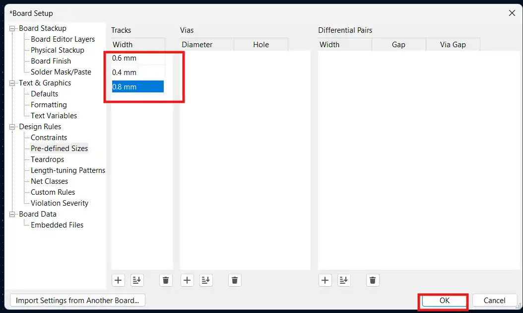
Before routing I set my trace widths. I went to the track width dropdown and clicked Edit Pre-defined Sizes.
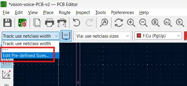
I added 0.4mm, 0.6mm, and 0.8mm. Signal traces use 0.6mm and power traces use 0.8mm.
Then I routed everything by hand. Single sided board so everything had to connect without any vias. I kept the 100nF caps right next to the ADS1115 VDD pins so the decoupling traces stay short.
Step 3 — Exporting for Milling
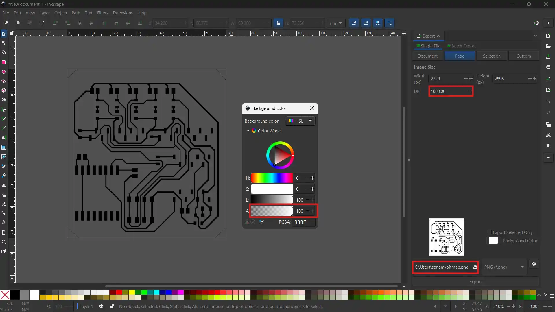
Same export process as the previous electronics weeks. File → Plot, SVG format, exported the F.Cu layer and Edge.Cuts layer separately.
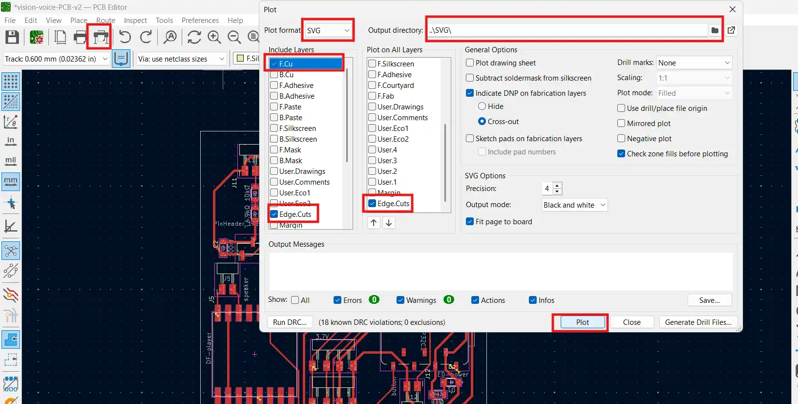
Opened the F.Cu SVG in Inkscape.
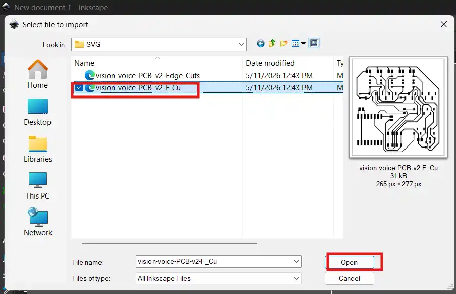
Set the export DPI to 1000 so Mods CE has enough resolution to read the traces properly.
Loaded both PNGs into Mods CE using the Roland SRM-20 mill PCB program.
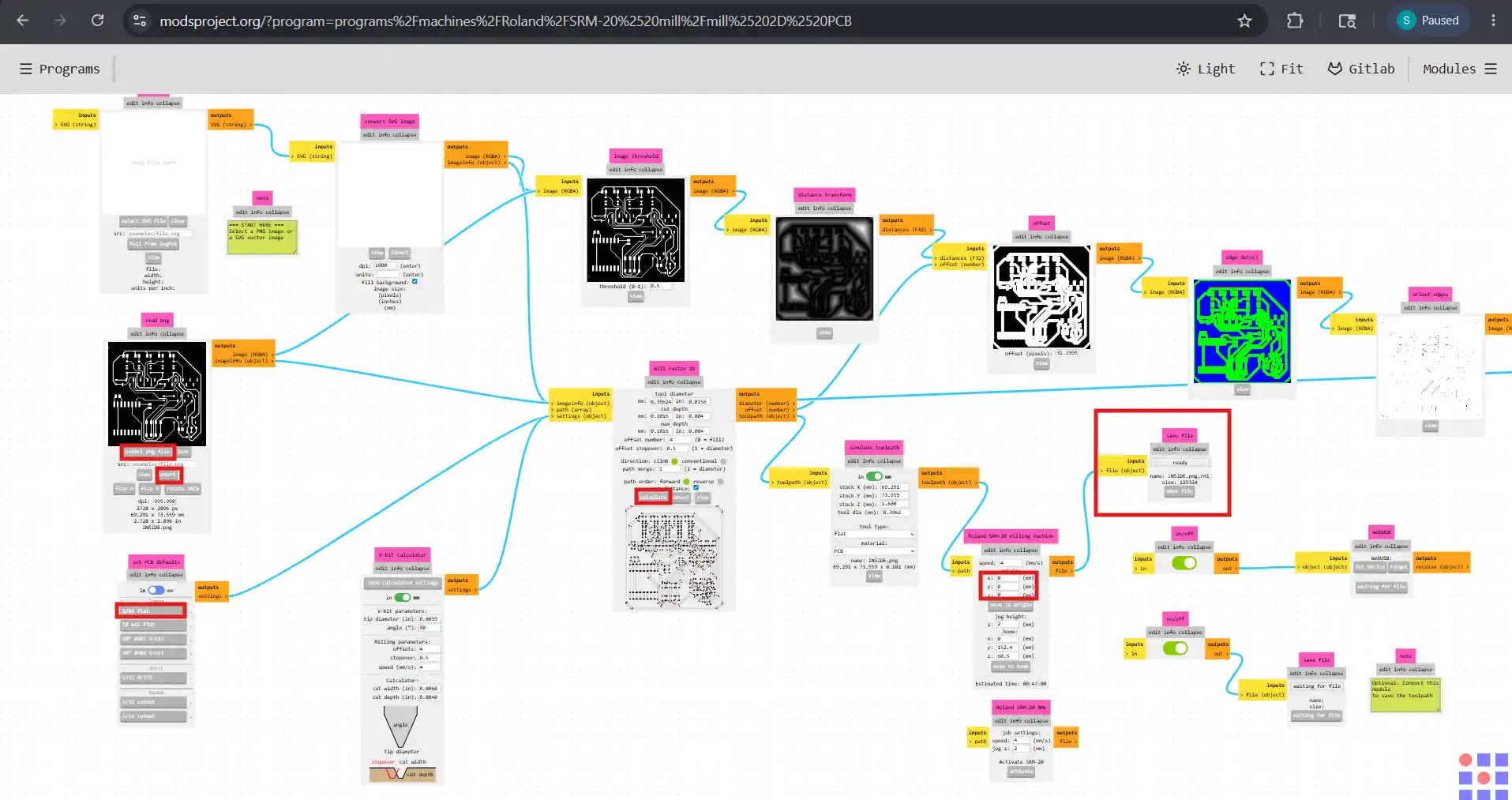
The colorized toolpath preview shows all the paths the mill will follow.
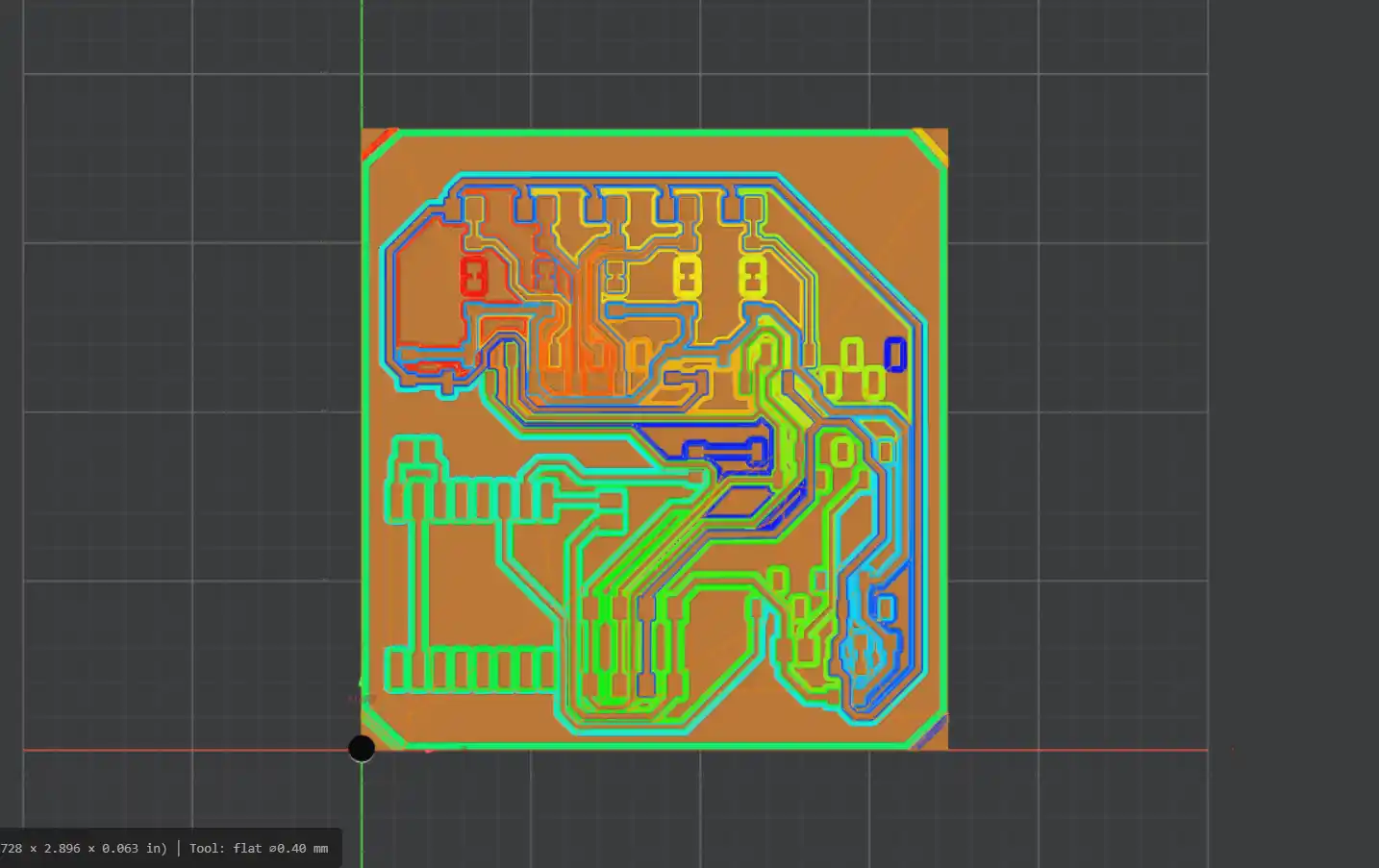
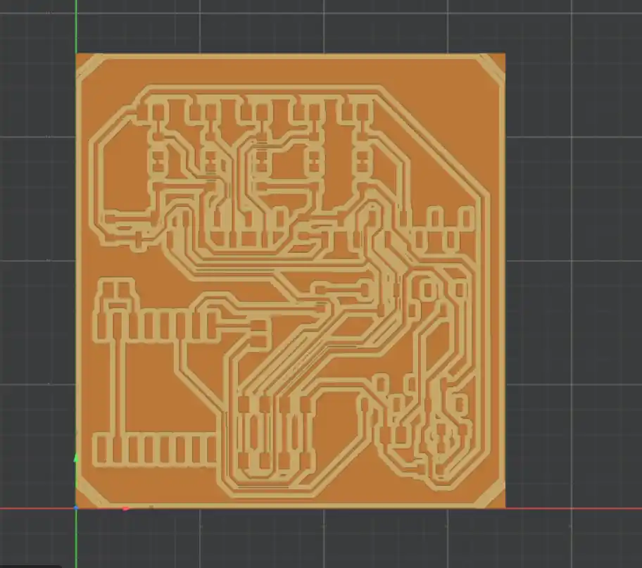
The 3D view confirmed everything looked clean and properly isolated.
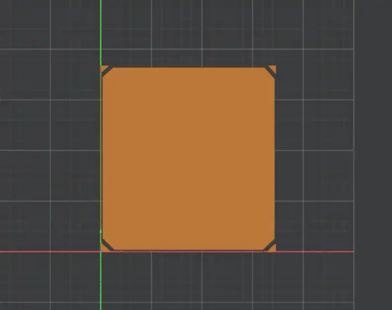
Generated a separate RML file for the edge cuts. The board outline has chamfered corners.
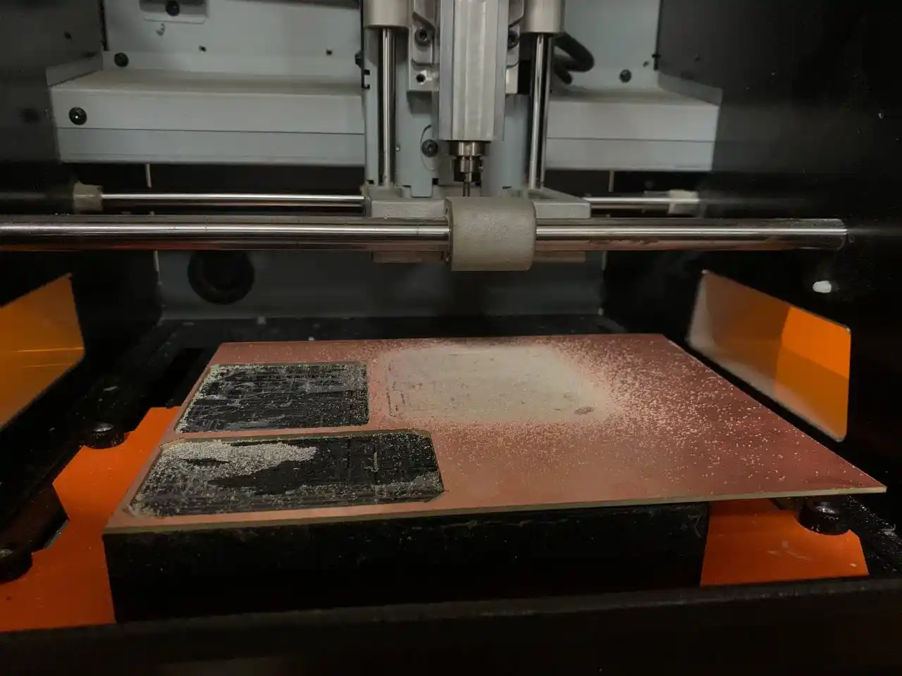
Step 4 — Milling
Sent the RML files to the Roland SRM-20 and started the mill.
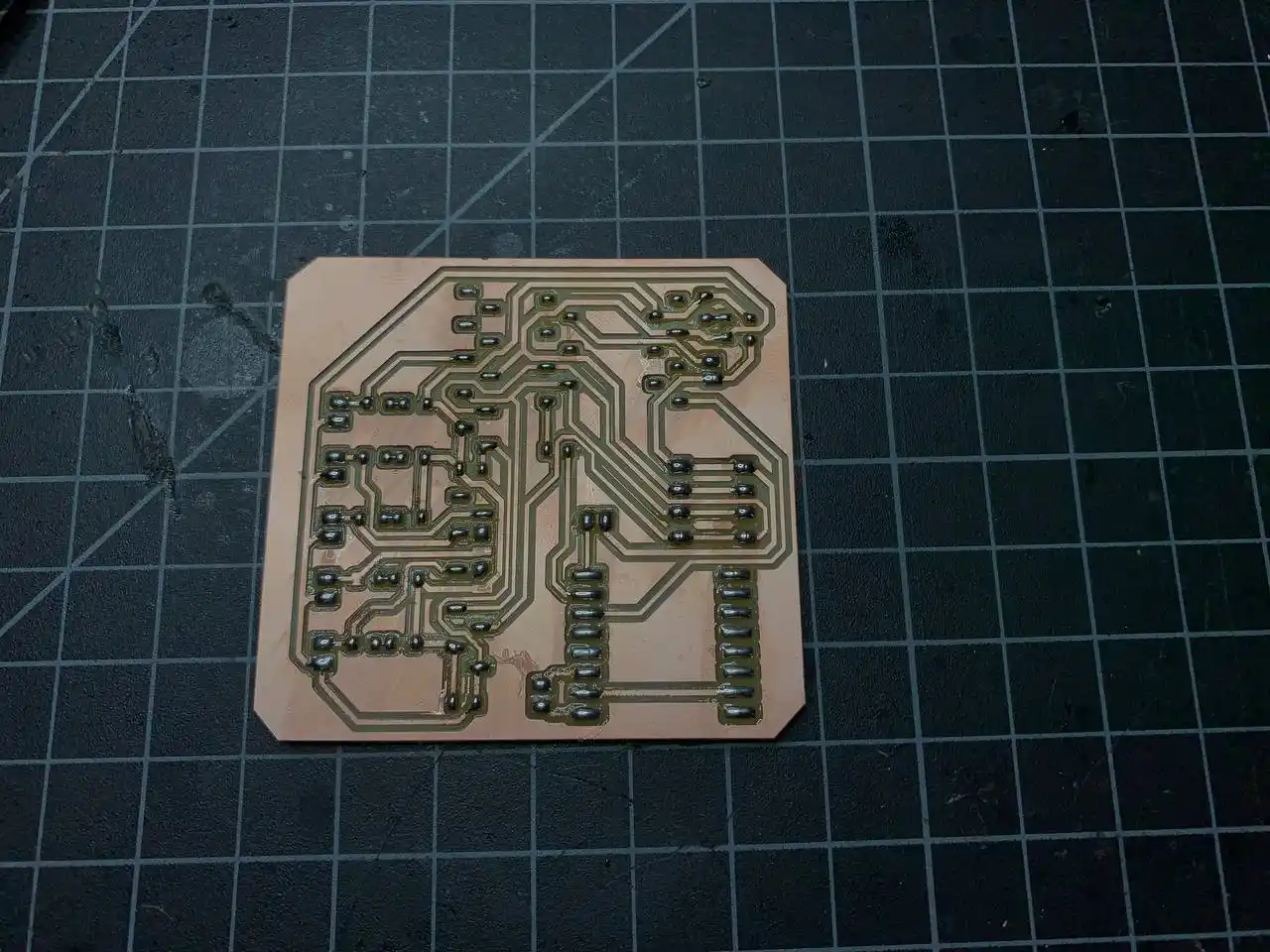
Right after milling, before cleaning.
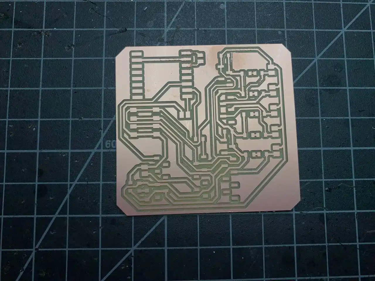
After cleaning. The traces came out really clean and I was honestly so happy with how it looked!
Step 5 — Soldering
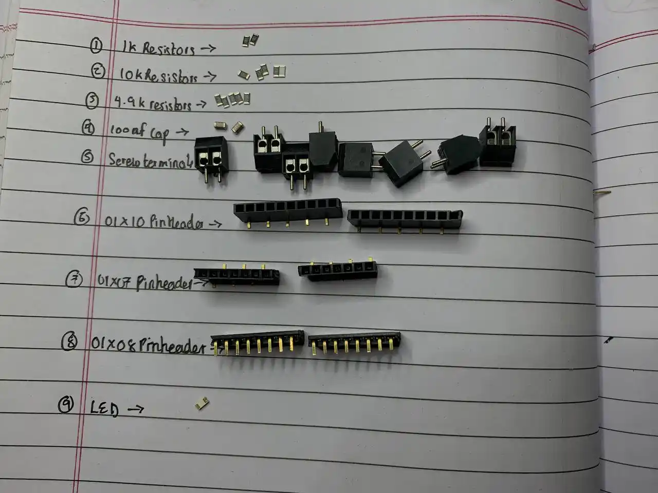
Before starting I wrote out every component in my notebook and laid all the parts out next to it so I wouldn't miss anything.
I started with the SMD components — resistors, capacitors, LED — since those need to go down before the pin headers and screw terminals can go on top.
Here is a timelapse of the full soldering session.
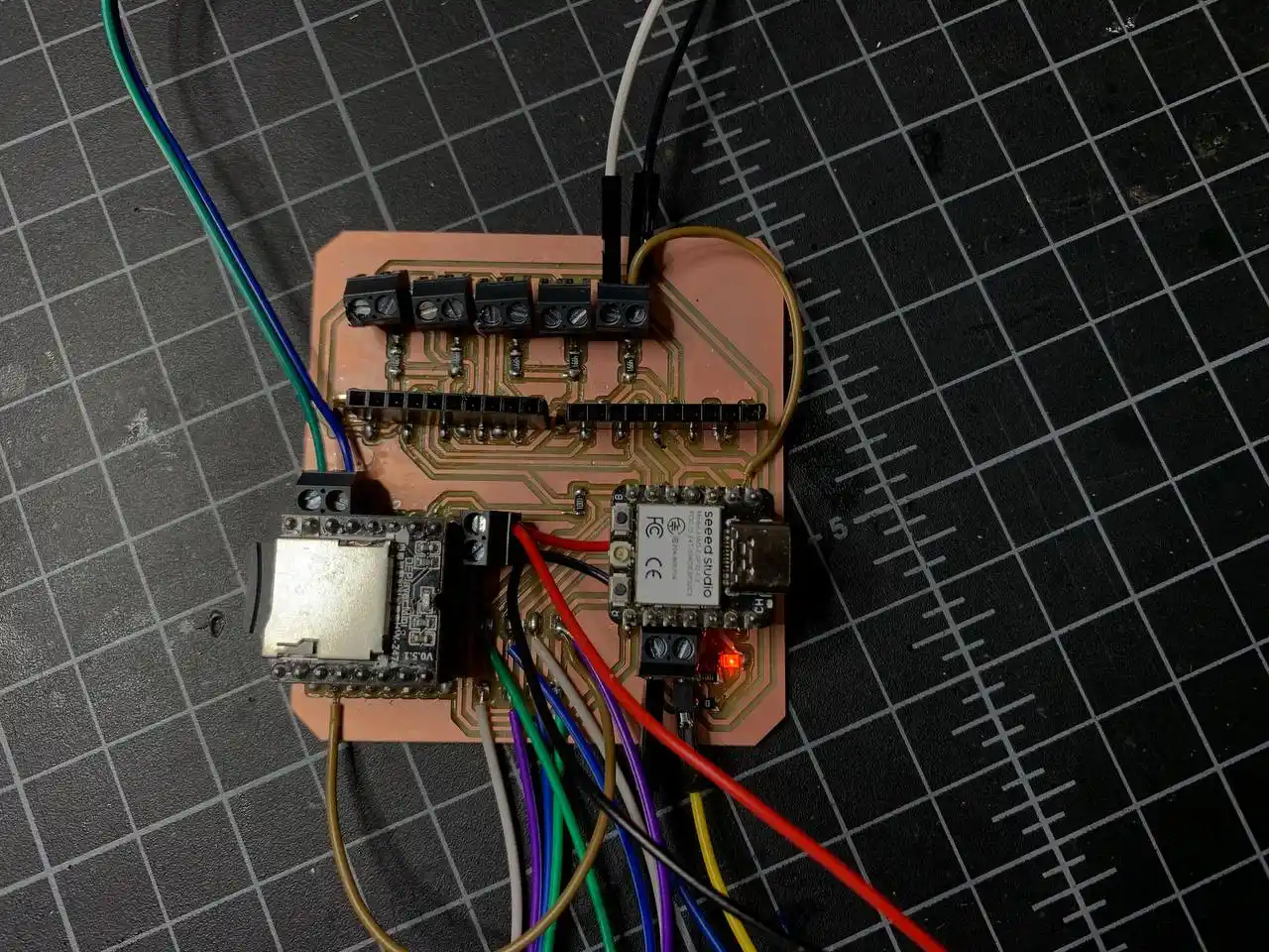
After all the pin headers and screw terminals were on and the XIAO and DFPlayer were plugged in, the red power LED came on as soon as I connected power. yay!! ^-^
Step 6 — Packaging
This is basically where everything gets a proper place instead of just floating around on a bench with jumper wires everywhere.
On the PCB itself every component is fixed and intentional — XIAO and DFPlayer sit in SMD female pin headers so they are secure but still removable, flex sensors connect through labeled screw terminals along the top edge, speaker and battery through screw terminals at the bottom, and the OLED and MPU6050 have dedicated solder pads. Nothing is loose. All components are organized around the PCB edges to keep the center clear for the mounting holes that attach to the enclosure.
For the full wearable, the layout is: OLED on the face of the wrist casing so the text is easy to read, MPU6050 on the back of the hand, flex sensors along the back of each finger with the wires bundled back down into the casing, speaker inside the casing, button coming through to the outside so it's accessible, and LiPo inside the casing. The USB-C port on the XIAO faces the right edge of the board so you can charge and reprogram without taking anything apart. The SD card slot on the DFPlayer faces the left edge so audio files can be swapped without disassembling.
Here is everything wired up to the PCB all together for the first time.
Step 7 — Testing
The ADS1115 modules haven't arrived yet so I short-wired one flex sensor signal pin directly to A0 on the XIAO — same as how I tested during the component testing phase. Everything else is properly connected through the PCB.
I uploaded the same combined sketch from the component testing phase and powered up with the LiPo.
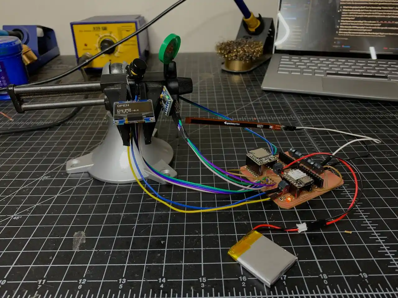
It worked first try! The OLED showed "OPEN" with the live flex and accel values updating, bending the sensor triggered the DFPlayer to play audio through the speaker, and the button worked for both short press and long press. Everything that worked on the breadboard now works through the real PCB. Really happy about this one!! ^-^
Here is the demo video.
The sketch used here is the same full combined sketch from the project development page.
Enclosure Design
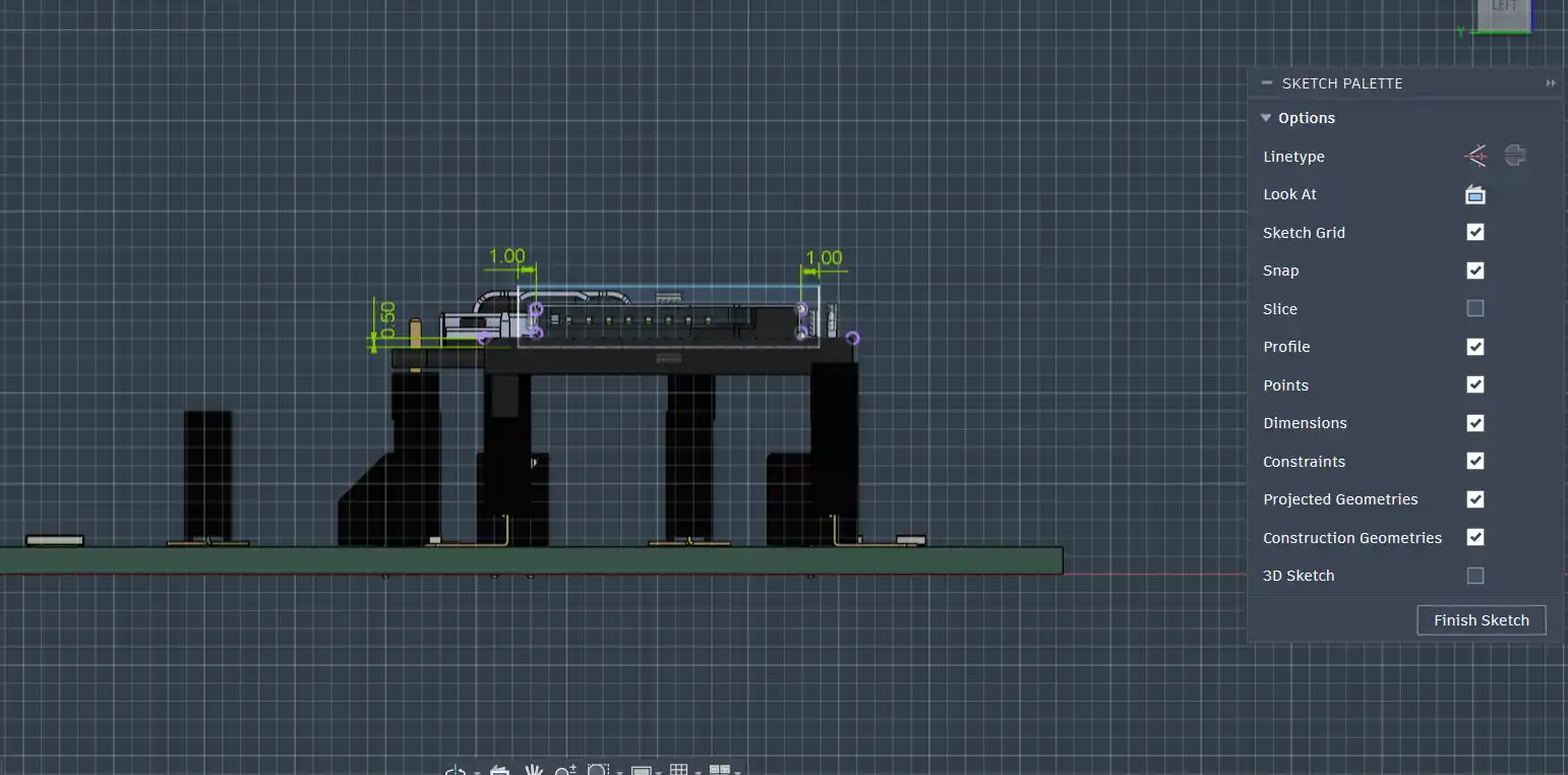
Once the PCB was done and tested I started designing the enclosure that everything lives in. I used Fusion 360 and started by importing the PCB as a STEP file so I could design the casing around the actual board dimensions.
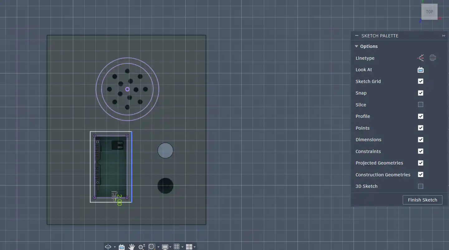
I sketched the base around the PCB footprint, extruded it to give it walls, then added mounting holes for the PCB, a slot for the SD card, and a hole for the USB-C port so I can charge and reprogram without opening anything.
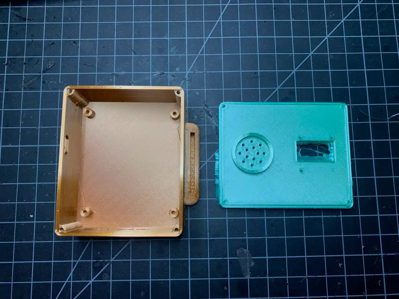
The lid has cutouts for the OLED and speaker so they're accessible from outside. I also added side handles so the casing is easy to put on and take off.
After adding fillets to all the edges here is the final enclosure design:
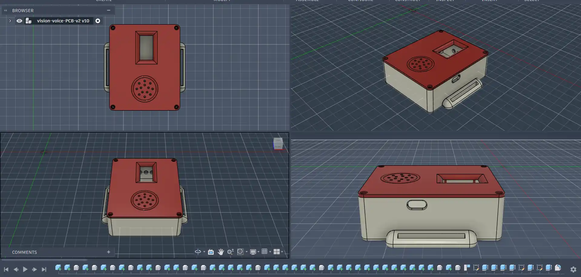
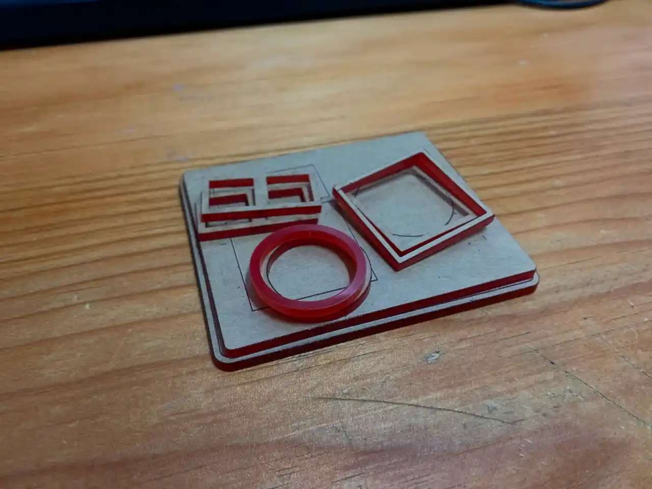
I 3D printed the base on a Prusa and laser cut the lid from acrylic since I wanted it to be a bit thinner and tighter than what the printer could reliably do.
The enclosure design files are available here: Enclosure Design
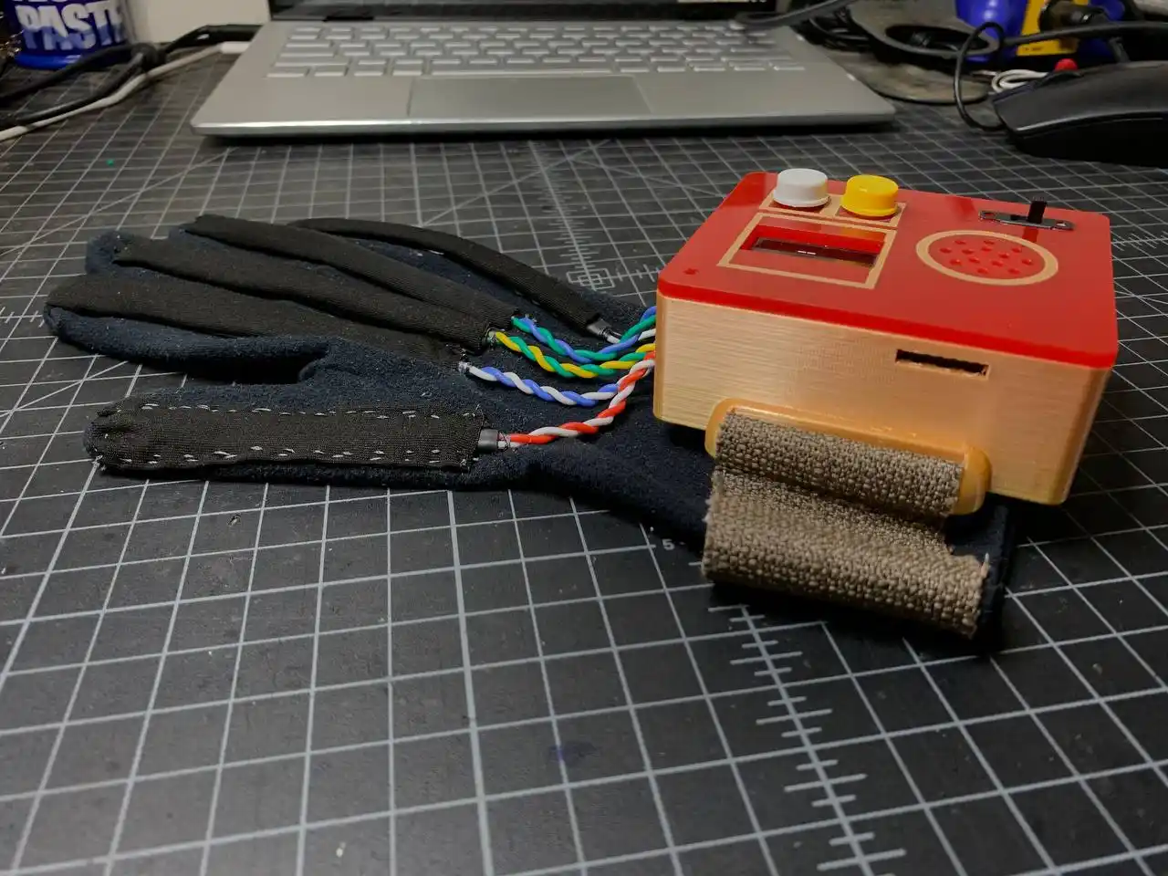
Glove Fabrication and Physical Integration
Before the final assembly I had to make the glove itself into a proper wearable platform. This involved sewing the flex sensors into place, creating an adjustable wristband, and managing the wiring so everything stays neat and flexible.
Sewing the Flex Sensors
I started by sewing fabric slots along each finger of the glove to hold the flex sensors in place. Each sensor slides into its slot so it stays positioned on the back of the finger where it can detect bending accurately.
The slots keep the sensors from shifting around when the hand moves, which is important because any movement would throw off the calibration and make the gesture recognition less reliable.
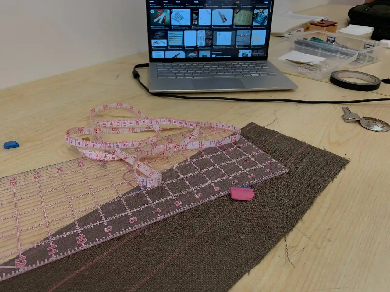
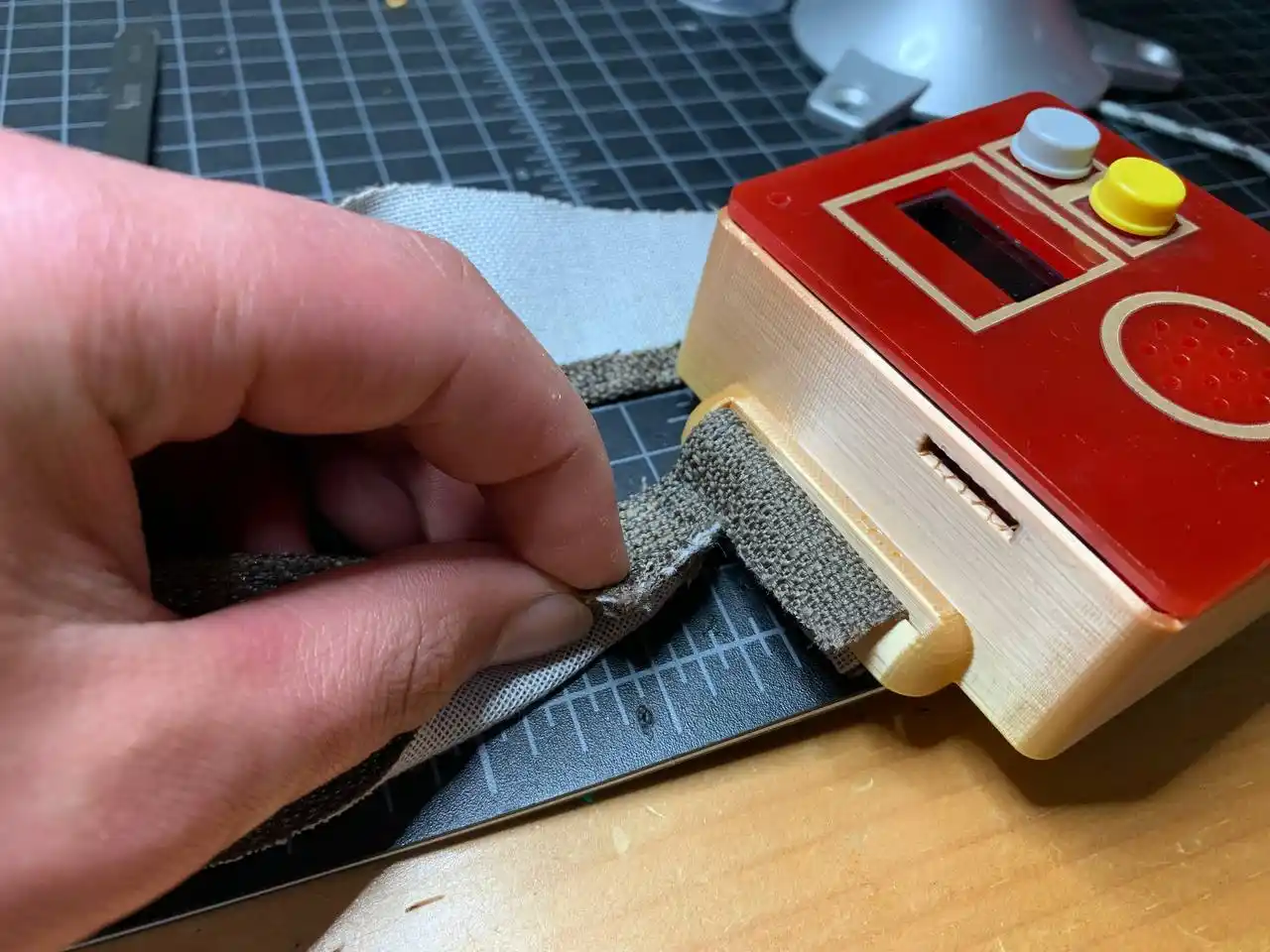
Making the Wristband
I measured and cut fabric for a wristband that would hold the enclosure against the wrist. My first attempt at the band wasn't adjustable, so I cut it, redesigned it, and sewed it again using Velcro to make it adjustable for different wrist sizes.
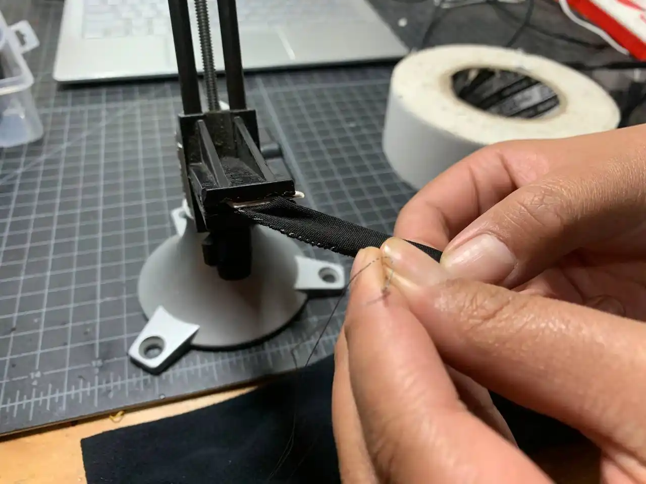
Wire Management
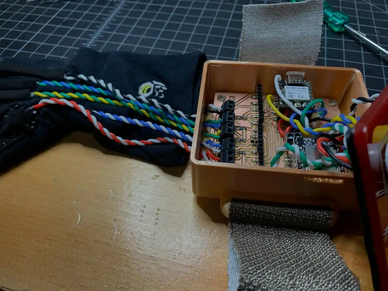
For the flex sensor connections I used silicone-insulated wires because they stay flexible and don't stiffen up. I braided the wires together to keep them neat and prevent tangling as they run from the fingers down into the wrist casing.
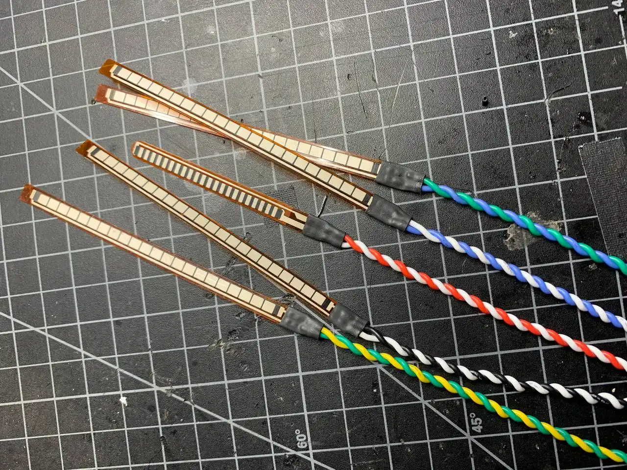
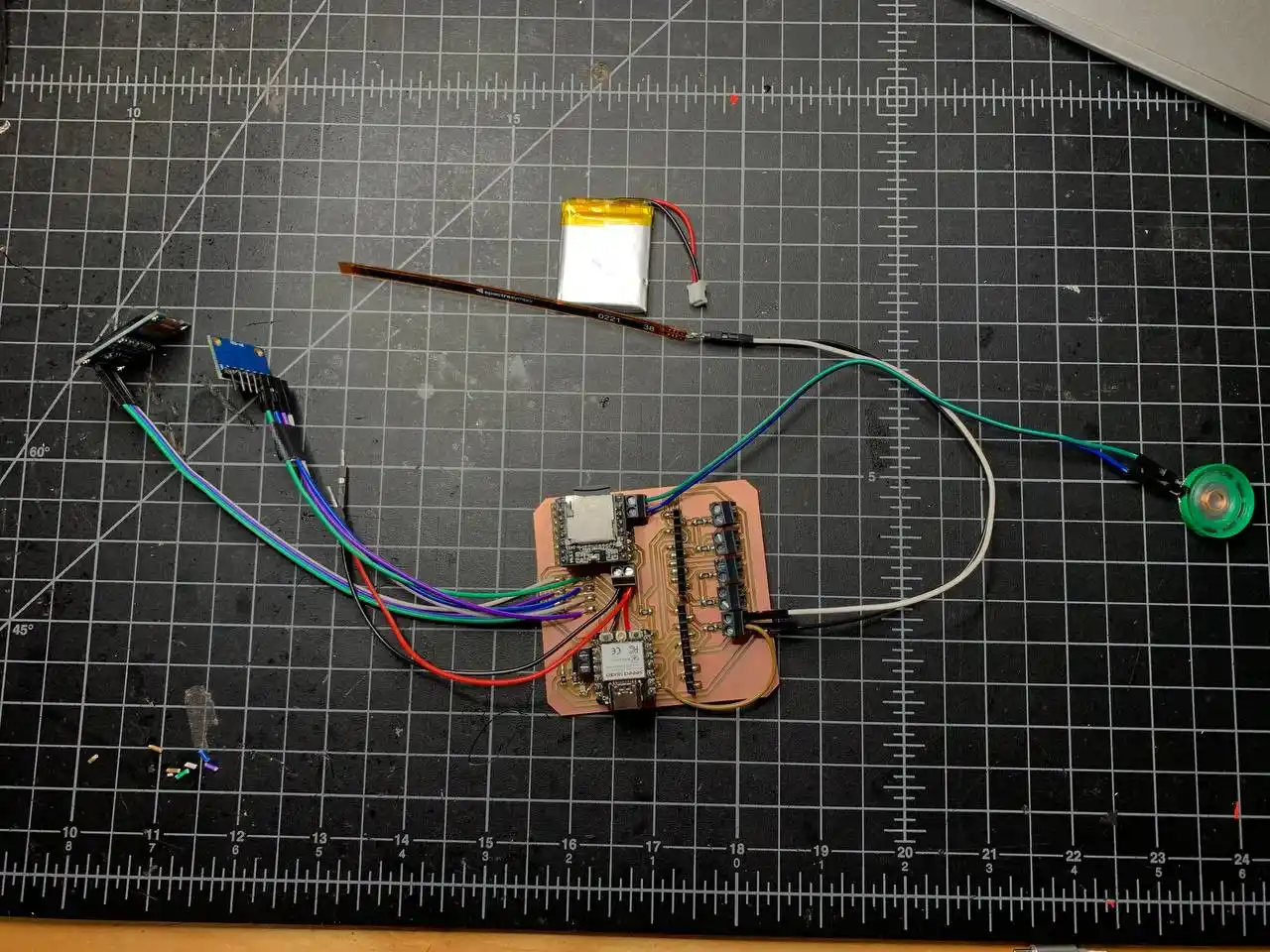
Here are the flex sensors connected to the PCB with the managed wiring:
Final Assembly
With the enclosure ready, the glove fabricated, and the PCB fully tested, I assembled everything together into the actual wearable.
The flex sensors are sewn into the glove fingers with fabric slots, the Velcro wristband attaches the casing securely, and the silicone-insulated wires keep the connections neat and flexible. The MPU6050 sits on the back of the hand, the OLED and speaker are accessible through the lid cutouts, and the button is reachable from outside the casing.
Here is the final glove:
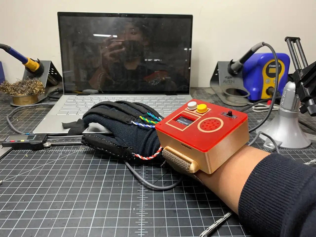
And it works!! Here is a demo of signing "ILY" (I Love You in ASL):
For the full project documentation including the kNN gesture recognition system, all code versions, and the complete assembly process, check the Vision Voice final project page.
What I Learned
I learned that system integration is not about doing everything at once. The PCB, the enclosure, the glove with its sewn in sensors and braided wires, and the adjustable wristband were all built and tested separately over time. This week was just about bringing them together and making sure they actually fit and work as one system. The full Vision Voice system is now one complete wearable, with the PCB, enclosure, glove, sensors, and all, and it is working. ^-^