Week 6 Electronics Design
Group Assignment
-
Use the testing equipment in the lab (such as oscilloscopes, logic analyzers, multimeters, etc.) and label the basic functions of each key part/control.
-
Observe the working status of the microcontroller circuit board and set the basic zero value (or baseline/reference).
-
Record and analyze signals, voltages, and communication data (input/output voltage, current, etc. Also, you can measure and calculate power consumption).
Testing equipment in Chaihuo
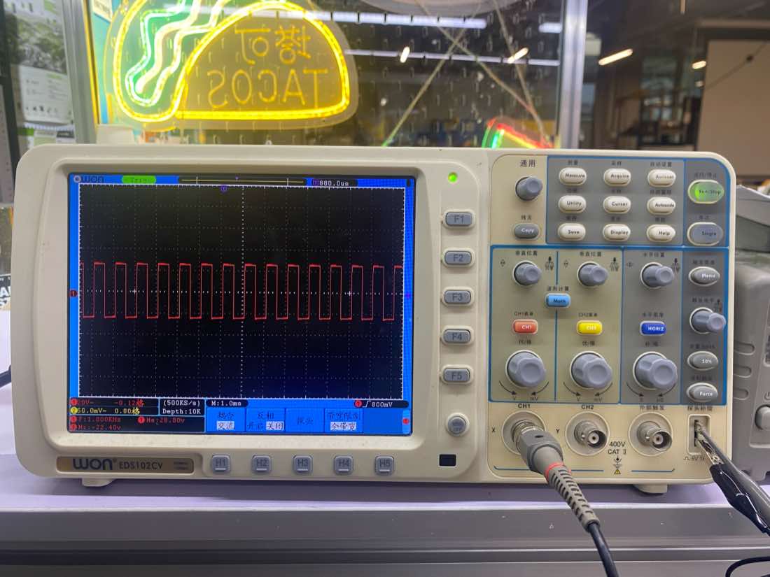
Oscilloscopes - OWON EDS102CV (100MHz/1GS a/s)
What is a Oscilloscopes ?
An oscilloscope is a versatile electronic measuring instrument. It converts invisible electrical signals into visible images, allowing people to study the changing processes of various electrical phenomena. Simply put, it acts like a "video camera that records voltage changes over time."
How does it works?
The core mission of an oscilloscope is to graph the relationship between Voltage and Time.
Acquisition: The probe connects to the circuit and captures the voltage signal.
Conditioning & Sampling: Internal amplifiers adjust the signal size, then an ADC (Analog-to-Digital Converter) converts the continuous analog voltage into a stream of digital data.
Storage & Processing: This data is stored in memory and processed by a microprocessor (calculating frequency, peak values, etc.).
Display: Finally, it plots the graph on the screen, where the horizontal axis (X-axis) represents time and the vertical axis (Y-axis) represents voltage amplitude.
Primary Uses:
Waveform Analysis: Observing if a signal has the expected shape (e.g., sine wave, square wave).
Parameter Measurement: Automatically measuring frequency, period, peak-to-peak voltage ($V_{pp}$), duty cycle, etc.
Troubleshooting: Looking for noise, voltage spikes, or signal distortion in a circuit.
Protocol Decoding: Advanced oscilloscopes can decode communication protocols like I2C, SPI, and UART to verify data integrity.
Timing Comparison: Comparing the time difference between two or more signals (e.g., trigger vs. response).
Main Parameters
| Term | Definition | Why it Matters |
| Bandwidth | The maximum frequency range at which the oscilloscope can accurately measure signals, typically measured in Megahertz (MHz). | Determines whether you can see high-speed signals clearly without distortion. |
| Sample Rate | The number of times per second the oscilloscope captures or samples the input signal, measured in Samples per second (S/s). | Higher sample rates provide a more detailed and accurate reconstruction of the waveform. |
| Trigger | A function that synchronizes the horizontal sweep of the oscilloscope to a specific point on the signal. | It stabilizes a repeating signal on the screen so it doesn't appear to be "drifting" or "jumping." |
| Vertical Sensitivity | The scale of the voltage axis, usually expressed in Volts per division (V/div). | Allows you to zoom in or out on the amplitude (height) of the signal. |
| Time Base | The scale of the horizontal axis, usually expressed in Seconds per division (s/div). | Allows you to speed up or slow down the view to see individual cycles or long-term trends. |
| Rise Time | The time it takes for a signal to transition from a low value (usually 10%) to a high value (usually 90%). | Critical for digital electronics to ensure pulses are sharp enough for the logic gates to read. |
| Memory Depth | The total number of data points the oscilloscope can store in a single acquisition. | A deeper memory allows you to capture long periods of time while maintaining a high sample rate. |
| Input Coupling | The method used to connect the signal to the oscilloscope (AC, DC, or Ground). | DC shows the whole signal; AC blocks the DC offset to let you focus on small ripples or noise. |
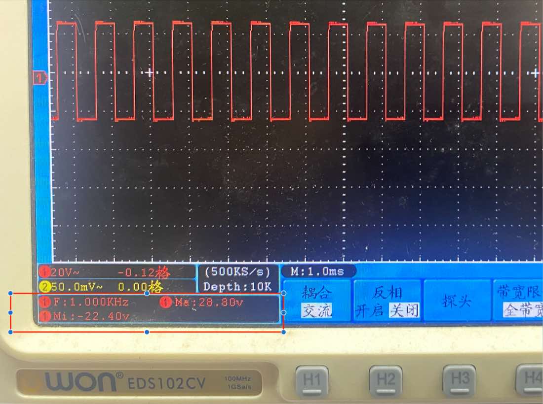
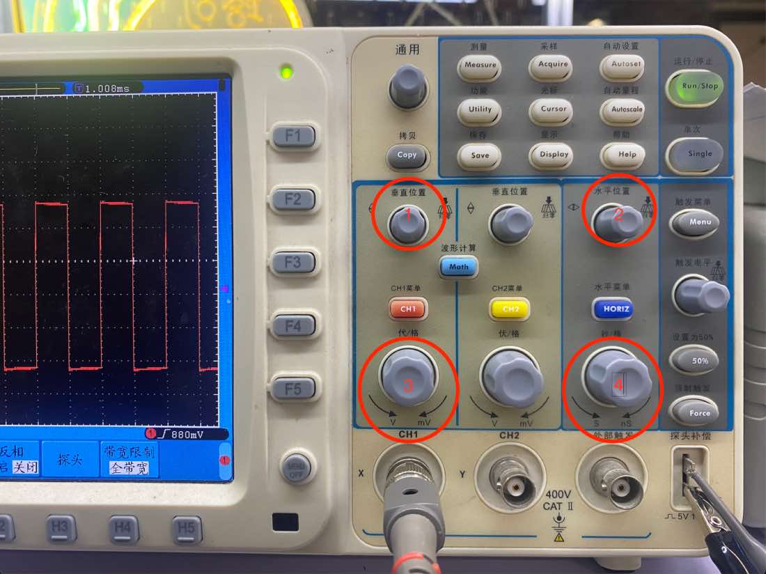
Learn the display pannel
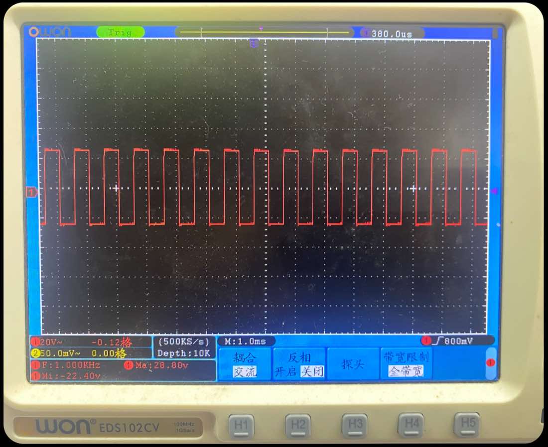
Part 1
| Information on the panel | Clarification |
| F: 1.000 KHz | the frequency of the signal is 1k Hz |
| Ma:28.80v | The max voltage of the signal is 28.8V |
| Mi:-22.40v | The minial voltage of the signal is -22.4v |
| VPP (Peak-to-Peak)( not in th image) | Ma-mi = 28.8 -(-22.4) = 51.2v |
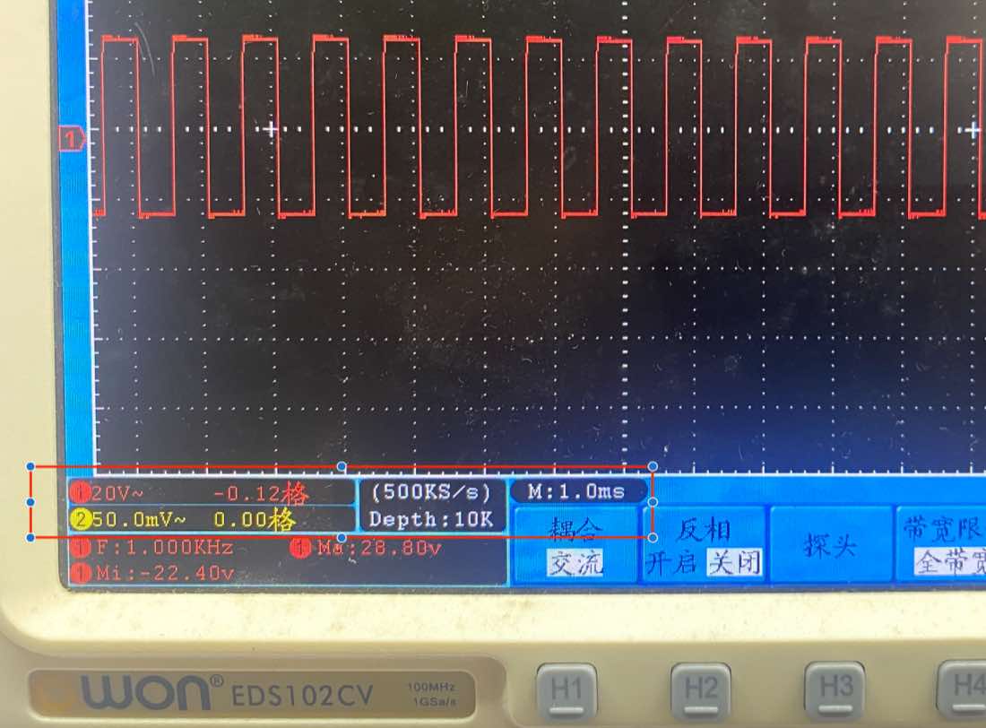
Part 2
| Information on the panel | Clarification |
| 20v~ | In the vertical, each row means20V; ~ means AC coupling; so the voltage is around 2.5rows, it is around 50V |
| M:1.0ms | In horizontal,each column means 1.0ms. The cycle of the wave is almost 1.0ms,therefore the Frequency is 1/1.0ms =1K Hz, same with data above |
| 500ks/s | Sample rate, 500k data point every second |
| Deepth 10K | Memory Depth,captures and stores 10,000 sampling points in a single acquisition cycle. |
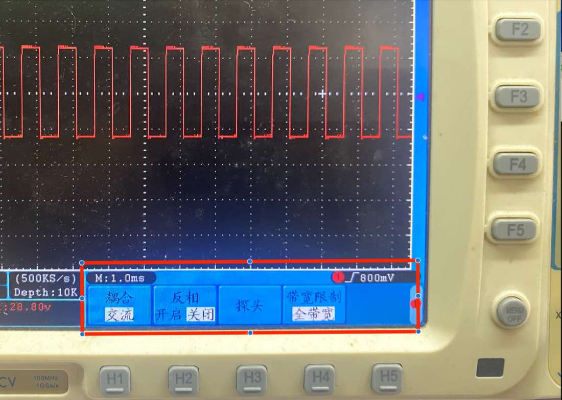
Part 3
| Information on the panel | Clarification |
| 耦合(Coupling) | AC couping, means remove the part of DC in the signal |
| 反相 (invert) | If turn on, the wave will invert |
| 探头 | NA |
| 带宽限制(bandwidth Limit) | 全带宽,show all the bandwidth, no limit, there is another option is 20MHz |
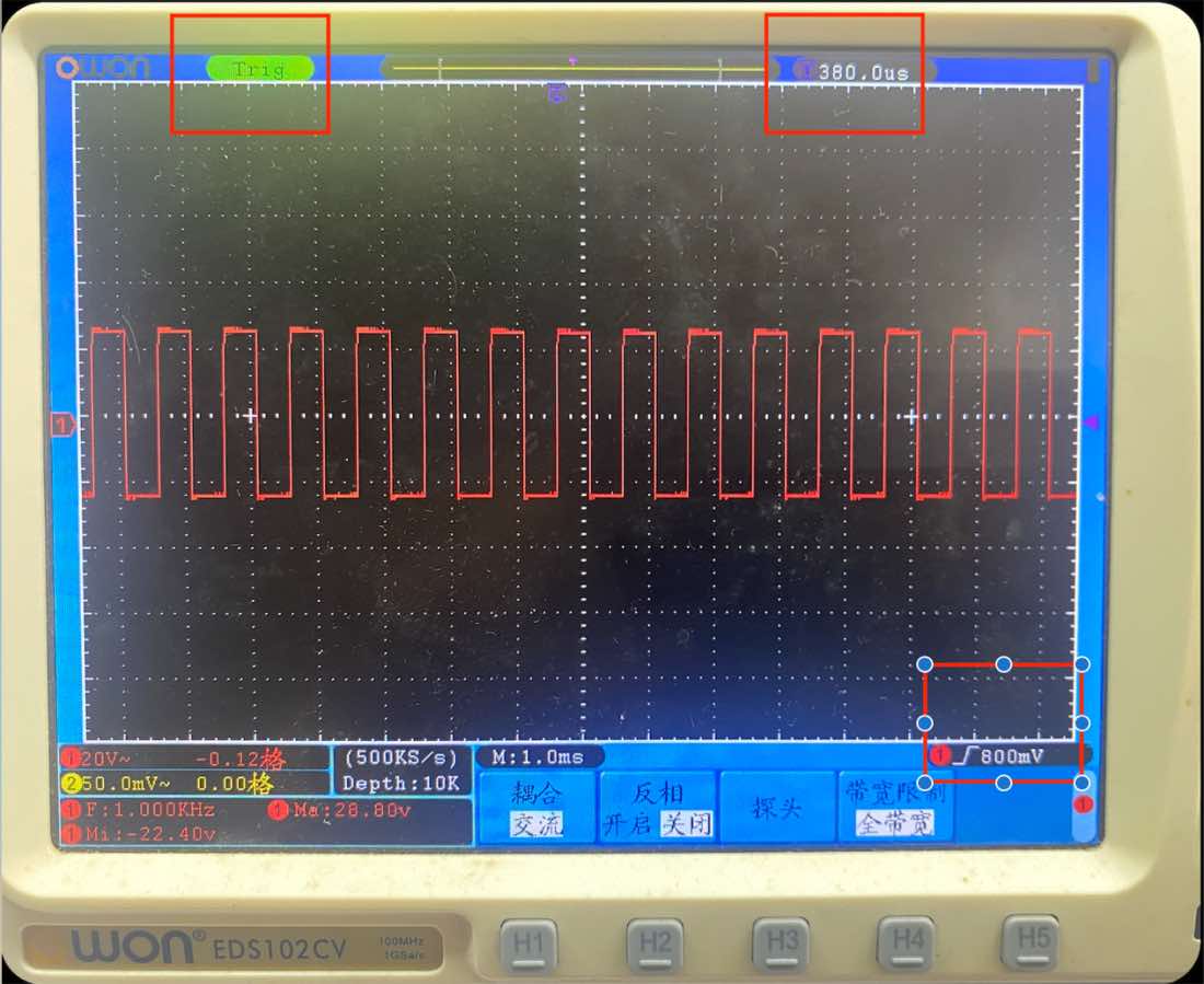
Part 4
| Information on the panel | Clarification |
| Trig | The signal has been captured and in the best condition to analyze |
| T 380.0 us | Horizontal DelayShows the time offset between the trigger point and the screen center. |
| 800mv | Trigger Level Set the voltage threshold to stabilize the waveform. The picture, the wave is happening at 800mv |
Control panel
| Button in the picture | clarification |
| 1 | Move the wave in vertical, like easy to calculate the voltage |
| 2 | Move the wave in horizontal,the trigger time will be adjust accordingly |
| 3 | Adjust Voltage of each row, to find the best analyze status |
| 4 | Adjust the time of each square, to find the best analyze staus |
Multimeters -HuaShengChang DT660B
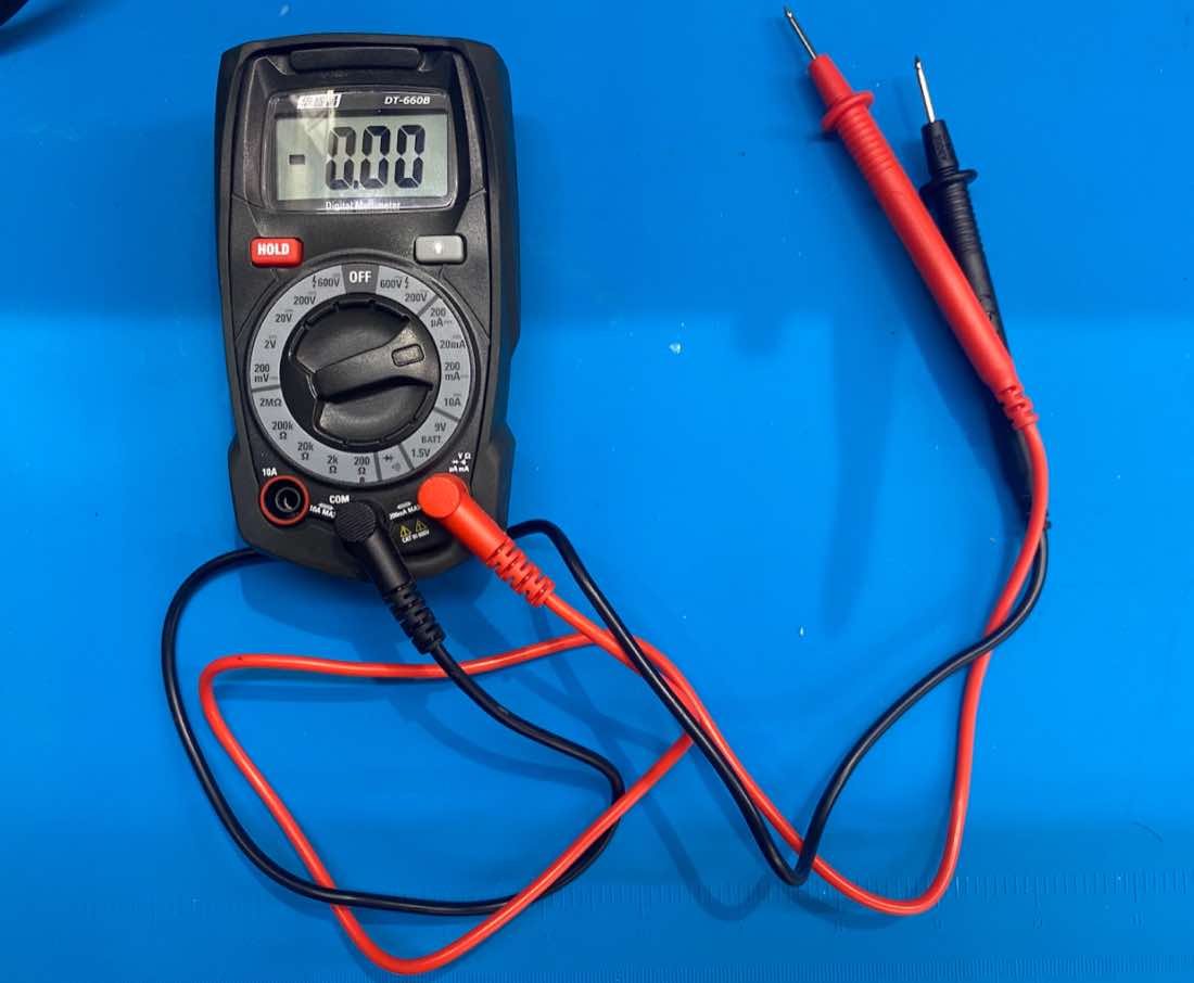
| Section | Symbol/Position | Description |
| DC Voltage | V… (200m to 600V) | Used for batteries and DC circuits. Select a range higher than your target voltage. |
| AC Voltage | V∼ (200 to 600V) | Used for mains electricity (wall outlets). Always use 600V for safety when testing outlets. |
| DC Current | A… (μA to 10A) | Measures current. Caution: Must move the red probe to the 10A port for high current. |
| Resistance | Ω (200 to 2M$\Omega$) | Measures resistors. The ⋅)) icon is for continuity (beeping). |
| Battery Test | BATT (1.5V / 9V) | A specialized mode to test small batteries under a slight load. |
| Diode Test | →+ | Checks if a diode is working. |
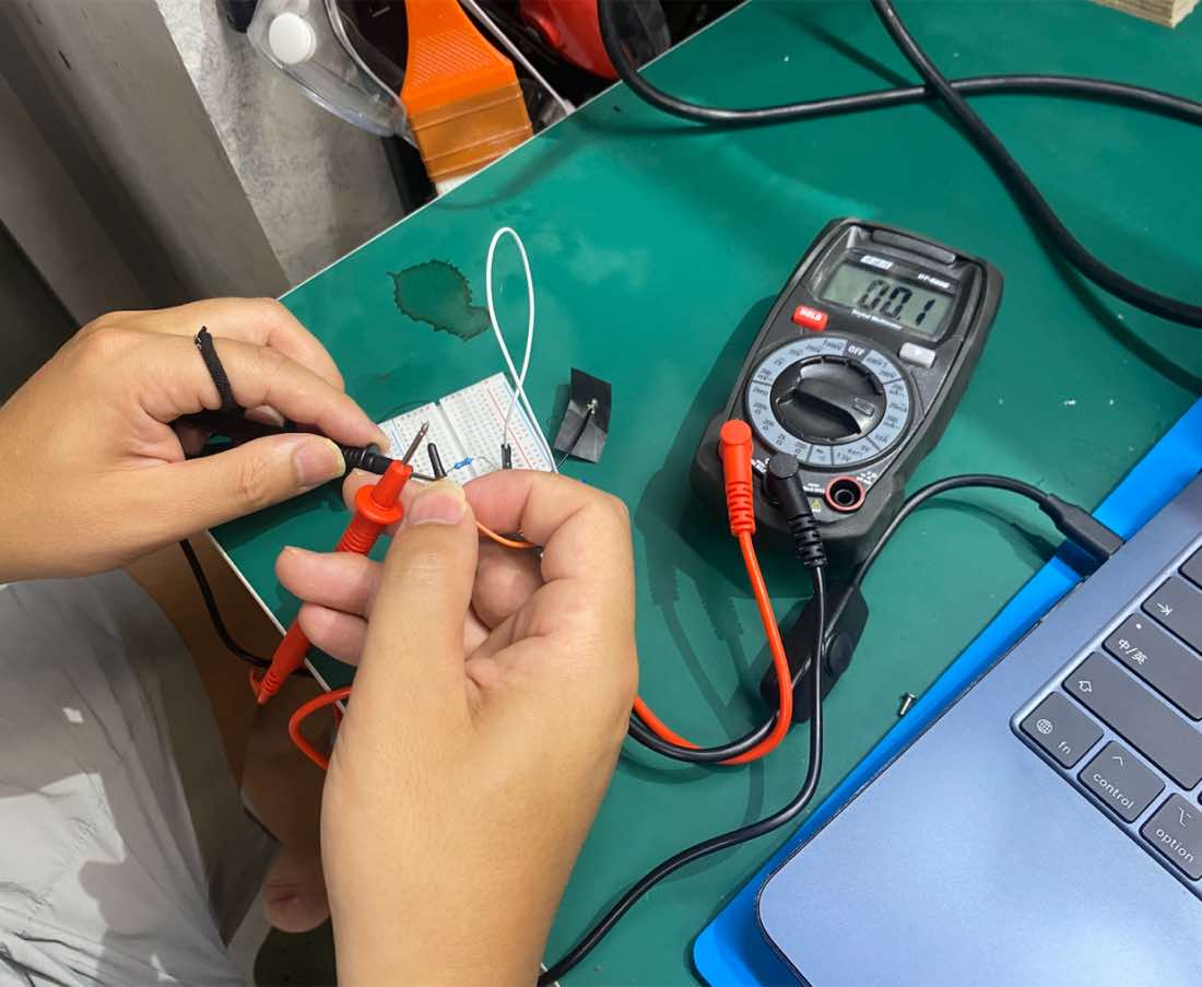
Do measurement, I build a simple circuit on bread board. I use the power supply with 3.3 V
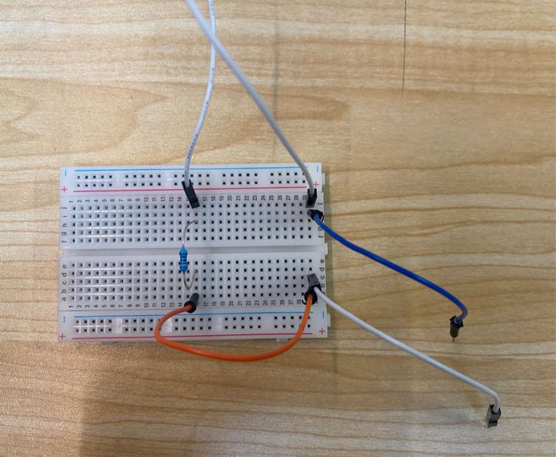
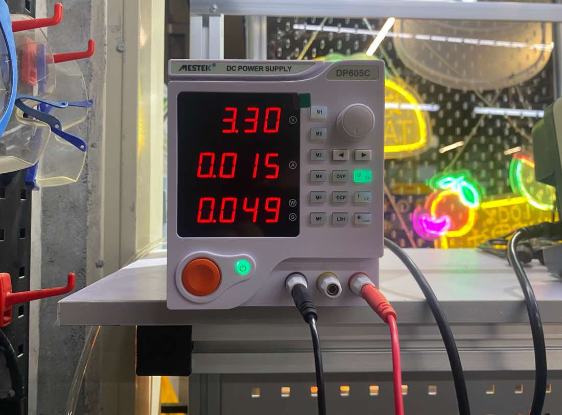
Measure current, the current is 0.01 A, there is different with 0.015A, it cannot show more digit.
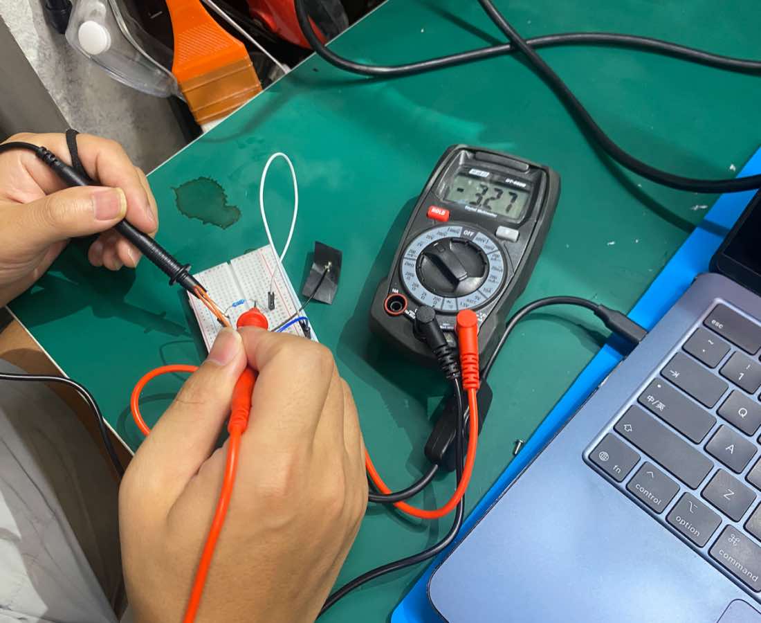
Measure voltage, the Voltage is 3.27V, close the power supply 3.3 V
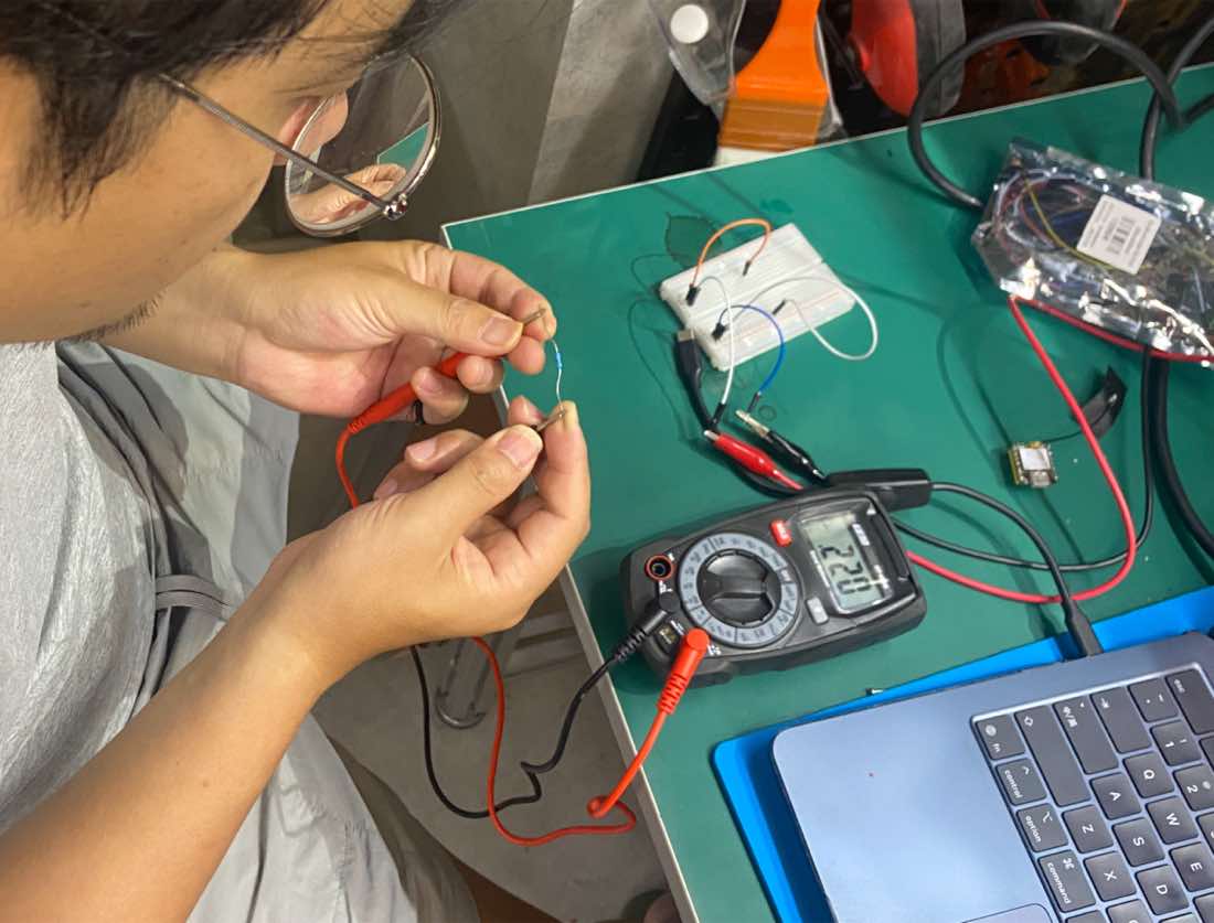
Measure resistor, the resistor is 220 Ω
Measure circuit ( small video)
Individual Assigement
- Try using different EDA tools (such as KiCad, Eagle, Altium Designer, etc.) and choose one.
a. Explain what you learned, and briefly describe the tool and its common uses.
- Use the EDA tool to design a development board that can interact and communicate with a microcontroller, including:
a. A controller (RP2040, ESP32, or you can directly use the XIAO series).
b. An input component (sensor, etc.).
c. An output component (LCD, etc.).
d. Communication capability (based on the controller's capabilities, e.g., ESP32-C3 has Bluetooth/WiFi).
e. It is best to design it as a board for your own final project, using components available in the fab lab's inventory (Fab Electronics Library for KiCad).
f. Upload the design files to your own webpage.
- Provide a complete "hero shot" of the final design diagram.
EDA Software
KiCad VS Autodesk vs EasyEDA
| Dimension | KiCad | Autodesk Eagle (Fusion) | EasyEDA |
| Philosophy | Open-Source Powerhouse: The global standard for open hardware. | Industrial Integration: Seamless bridge between MCAD and ECAD. | Efficiency First: Cloud-based tool for rapid prototyping. |
| Licensing | Free & Open Source (GPLv3) | Subscription (Free for Students/Personal) | Free (Cloud-based) |
| Learning Curve | Moderate (Rigorous workflow) | Moderate/High (Complex UI) | Very Low (Intuitive) |
| Fab Lab Library | Native Support. Dedicated fab.kicad_sym available. | Good. Requires scripts to import Fab libraries. | Limited. Mostly relies on community or LCSC parts. |
| Routing Engine | Excellent. Features "Push-and-Shove" routing. | Solid. Industry-standard manual routing. | Basic. Suitable for simple to medium boards. |
| Offline Ability | 100% Offline. Great for lab environments. | Hybrid. Requires periodic cloud syncing. | Primarily Cloud. Requires internet access. |
| 3D Integration | Great. Built-in 3D viewer (VRML/STEP). | Superior. Fully integrated with Fusion 360 3D workspace. | Good. Basic 3D previews for component clearance. |
| Best For... | Fab Academy Students & Open-Source developers. | Product Designers & Professional Engineers. | Beginners & Rapid Prototyping (PCB Assembly). |
KiCad if: You want to follow the "official" Fab Academy path. It is the most used tool within the community, making it easier to get help from instructors and peers.
Fusion/Eagle if: Your project involves complex mechanical housing and you need to ensure the PCB fits perfectly into a 3D-printed or CNC-milled enclosure.
EasyEDA if: You are under a very tight deadline and want to avoid the "library management" hurdle, as it has a massive built-in database of parts.
In this assignment, I wanna try both KiCad, as KiCad is the “official” Fab Acamady path.
KiCad
Download and installation
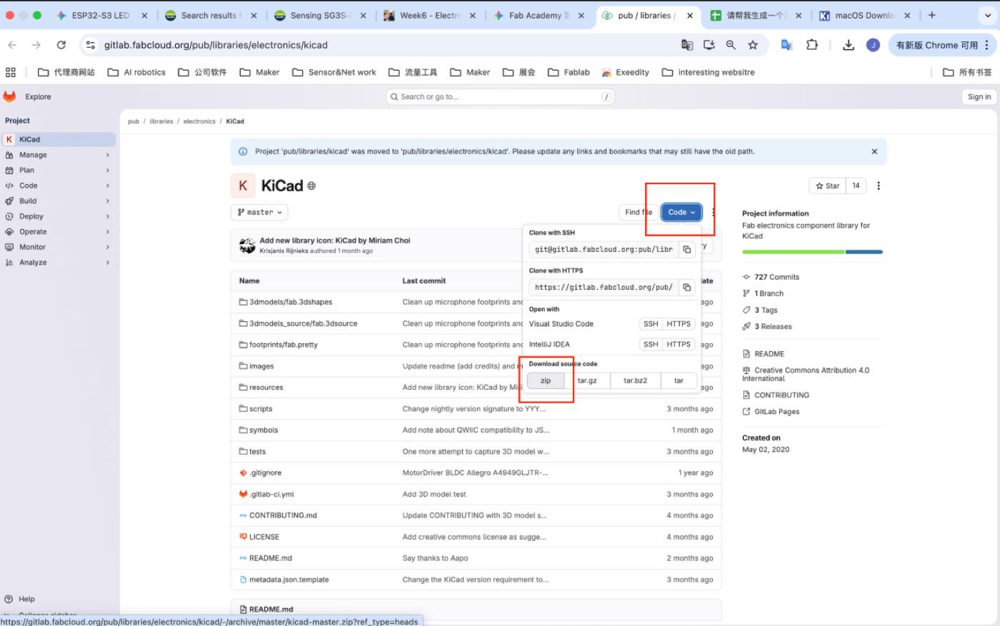
Download the KiCad component library and unzip
https://gitlab.fabcloud.org/pub/libraries/electronics/kicad
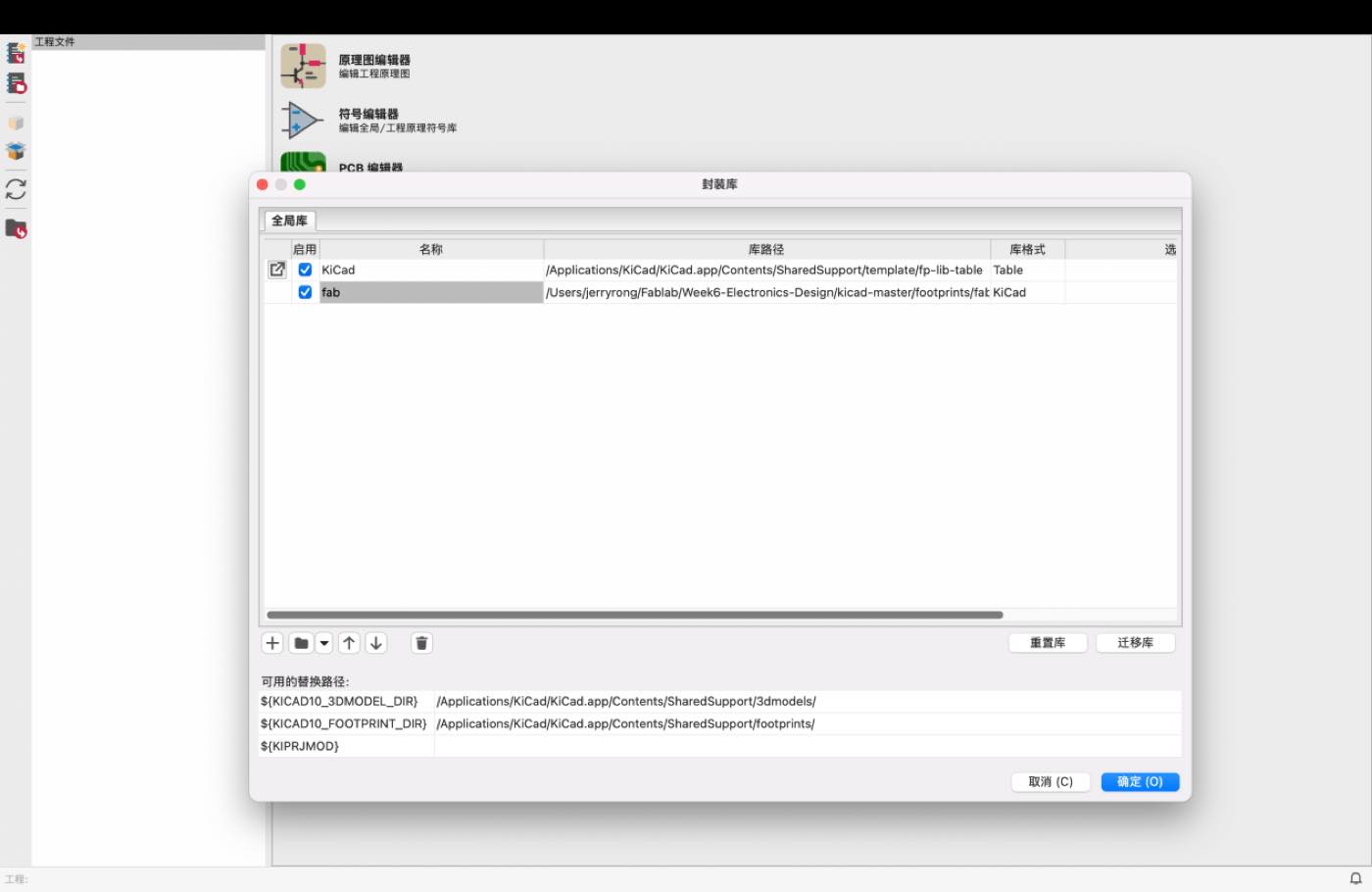
Add fab.Kicad_sym to Symbol libraries
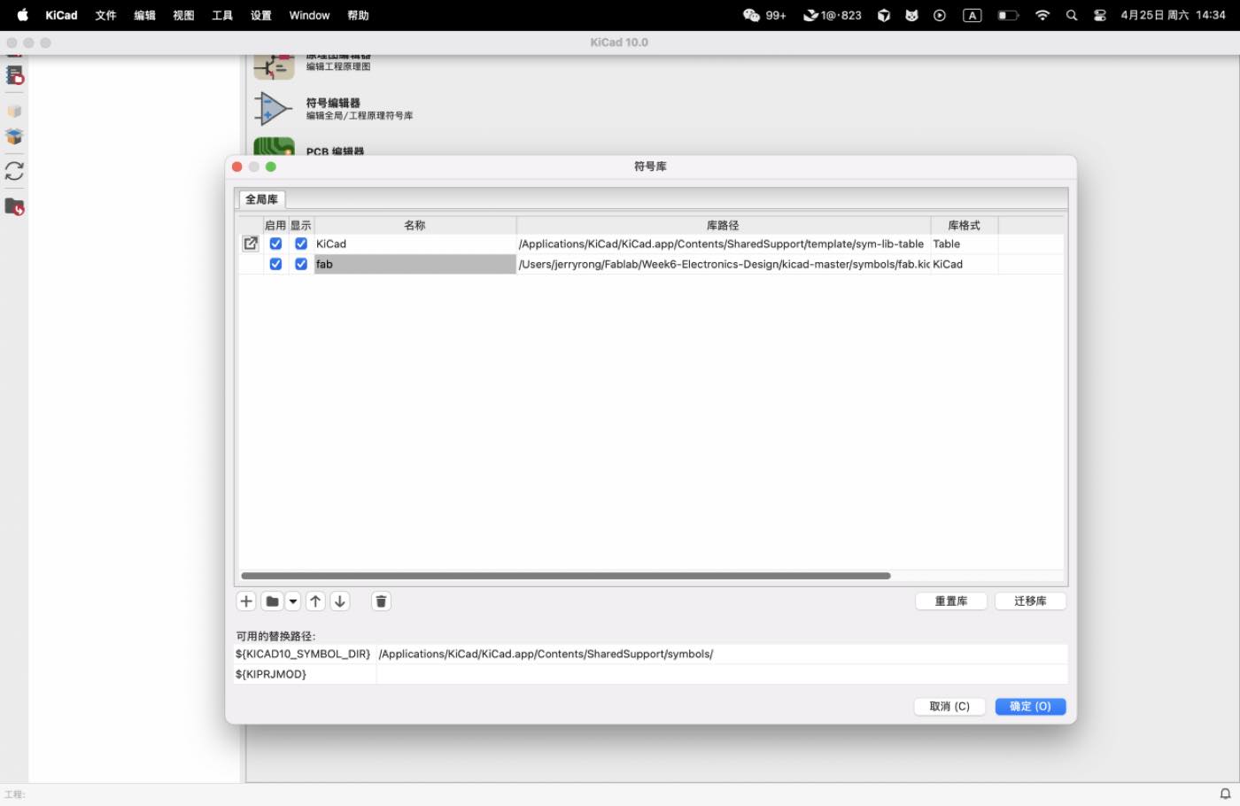
add fab.pretty to Footprint libraries
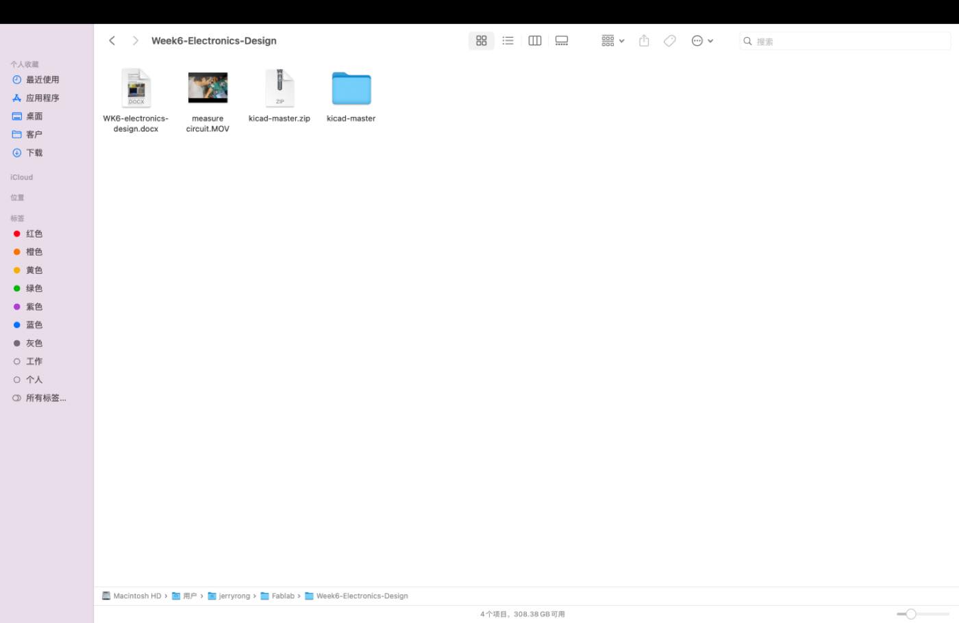
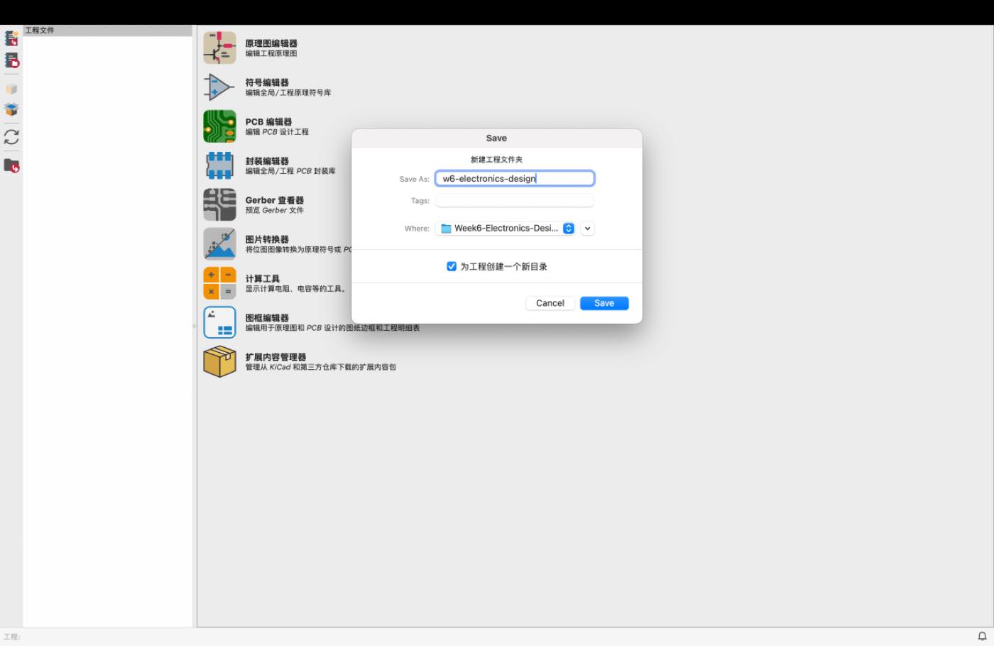
Start a folder and named with W6-electronic-design
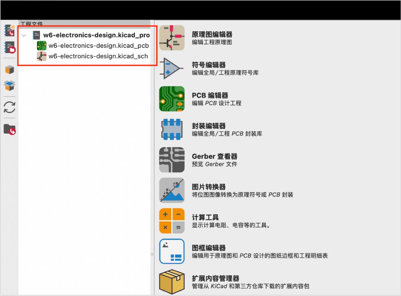
After creating the folder, 3 file below generated automatically, as blow
KiCad Essential Shortcuts (macOS Reference)
| Category | Shortcut | Action | Description |
| General | Space | Reset Local Coordinates | Sets the relative (0,0) point for measuring distances. |
| Z | Zoom to Fit | Resizes the view to show the entire design. | |
| Cmd + S | Save | Saves the current file. | |
| Esc | Cancel / Selection | Aborts the current tool and returns to the selection cursor. | |
| Schematic | A | Add Component | Opens the library to search and place a symbol (e.g., MCU, Resistor). |
| (Eeschema) | W | Wire | Starts drawing a logical electrical connection. |
| L | Label | Adds a Net Label to connect pins without drawing long wires. | |
| M | Move | Moves a component (breaks existing wire connections). | |
| G | Grab | Moves a component while stretching the wires to stay connected. | |
| R | Rotate | Rotates the selected component by 90°. | |
| V | Edit Value | Quickly changes the value (e.g., "499" for a resistor). | |
| C | Copy | Duplicates the selected component. | |
| PCB Layout | X | Route Track | Starts drawing a copper trace (wire) on the PCB. |
| (PCB Editor) | F8 | Update PCB | Imports changes/components from the Schematic to the PCB. |
| M | Move | Moves a footprint to position it on the board. | |
| D | Drag / Push | Moves a track while keeping it connected and pushing others aside. | |
| B | Fill / Refill | Updates copper pours (Zones) after making changes. | |
| V | Add Via | Creates a hole to jump between layers (Top to Bottom). | |
| U | Select Single Track | Selects one segment of a trace. | |
| I | Select Net | Selects the entire electrical path (the whole "net"). | |
| Alt + 3 | 3D Viewer | Opens the 3D preview of your board. |
Individual assignment
Make a expansion board for Xiao ESP32-C3, with a swtich as “ input” and LED as “output”. In assignment Week 4, I already run a similar project, lightening the LED, the difference is adding 1 one more switch”.
The Logic, when the button pushed, the LED Light on, or light off.
Step 1, I will use the Wokwi and build the Circuit first, and test it with Code. the Code generated by Gemini, and revise to the right pin no.
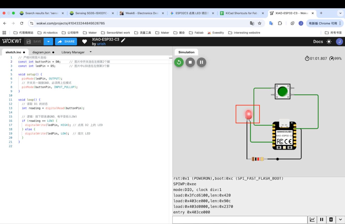
Code as below
const int buttonPin = D0; // 图片中开关连在左侧第1个脚
const int ledPin = D5; // 图片中LED连在左侧第6个脚
void setup() {
pinMode(ledPin, OUTPUT);
// 开关另一端接GND,必须用上拉模式
pinMode(buttonPin, INPUT_PULLUP);
}
void loop() {
// 读取 D1 的状态
int reading = digitalRead(buttonPin);
// 逻辑:按下即连通GND,电平变低(LOW)
if (reading == LOW) {
digitalWrite(ledPin, HIGH); // 点亮 D2 上的 LED
} else {
digitalWrite(ledPin, LOW); // 熄灭 LED
}
}
Part list in the circut
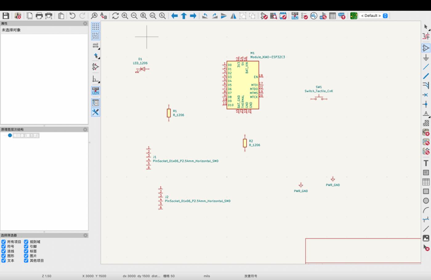
For the components will be involved, Xiao ESP 32 C3, LED, Resistor, switch, pinsocket for Xiao EPS 32 C3.
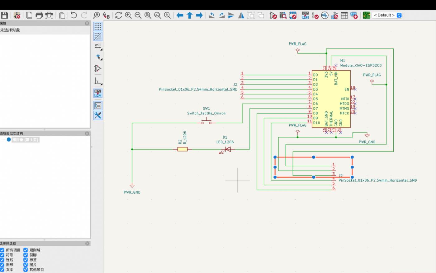
Step 2 Drawing the schematic
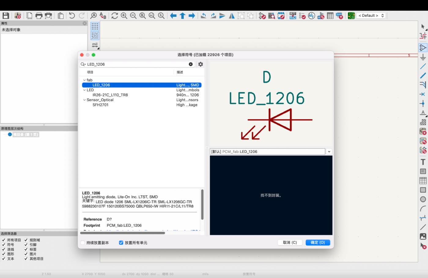
Find and add the parts to the schematic
Press “A” as the shortcut to add parts.
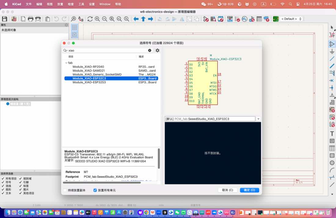
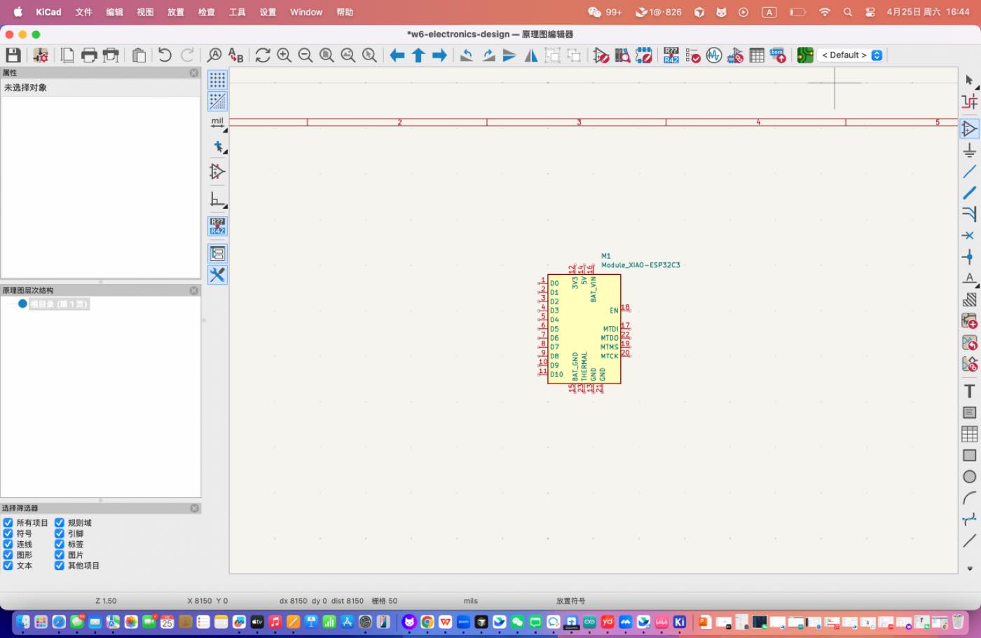
The same operation to add LED/ Switch/Resistor/pin sockets, as below
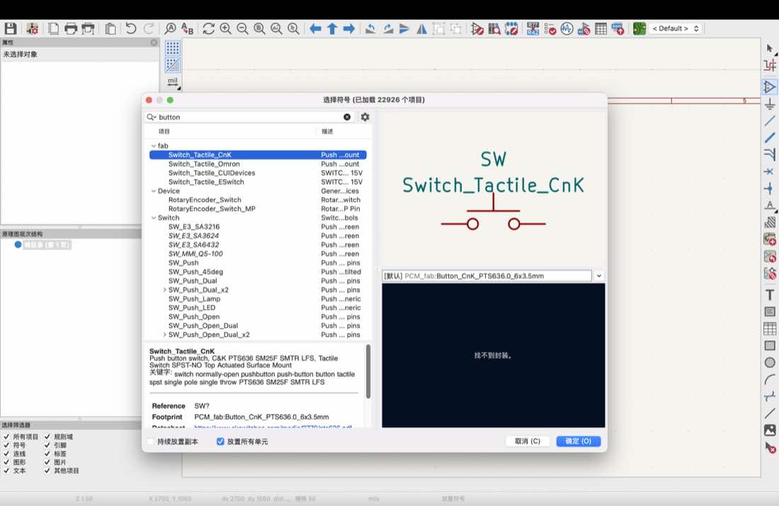
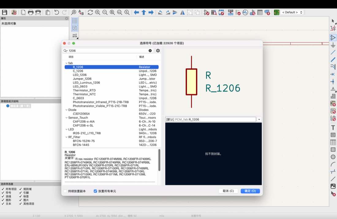
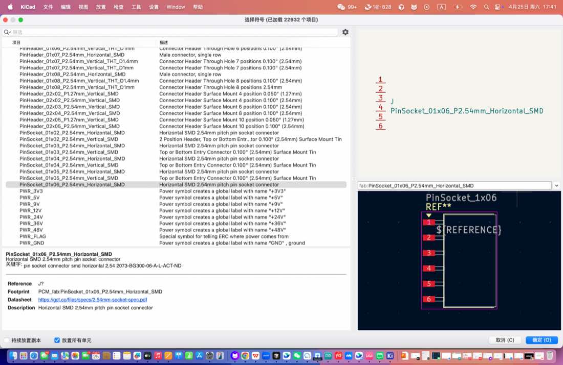
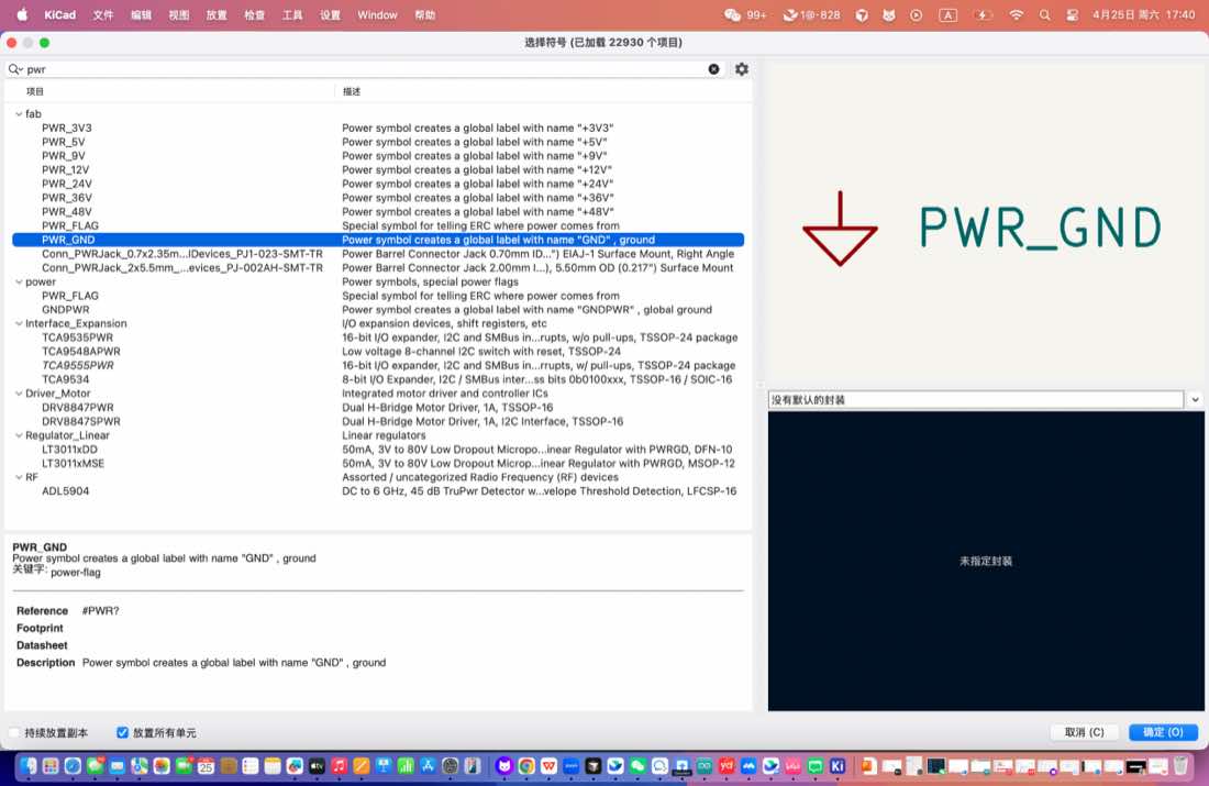
To product the circuit, add 1 more resistor to the Switch.
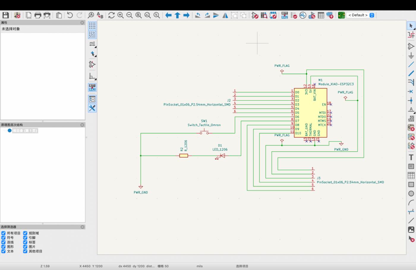
Step 3 connect all the parts.
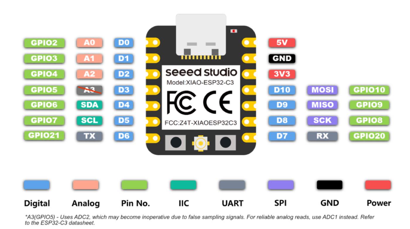
Refer the pin of Xiao ESP 32 C3
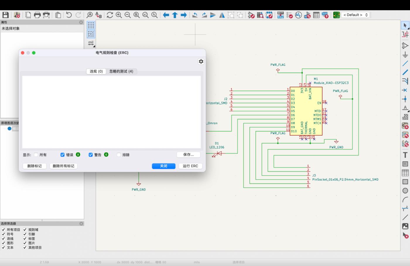
Step 4 run ERC to check
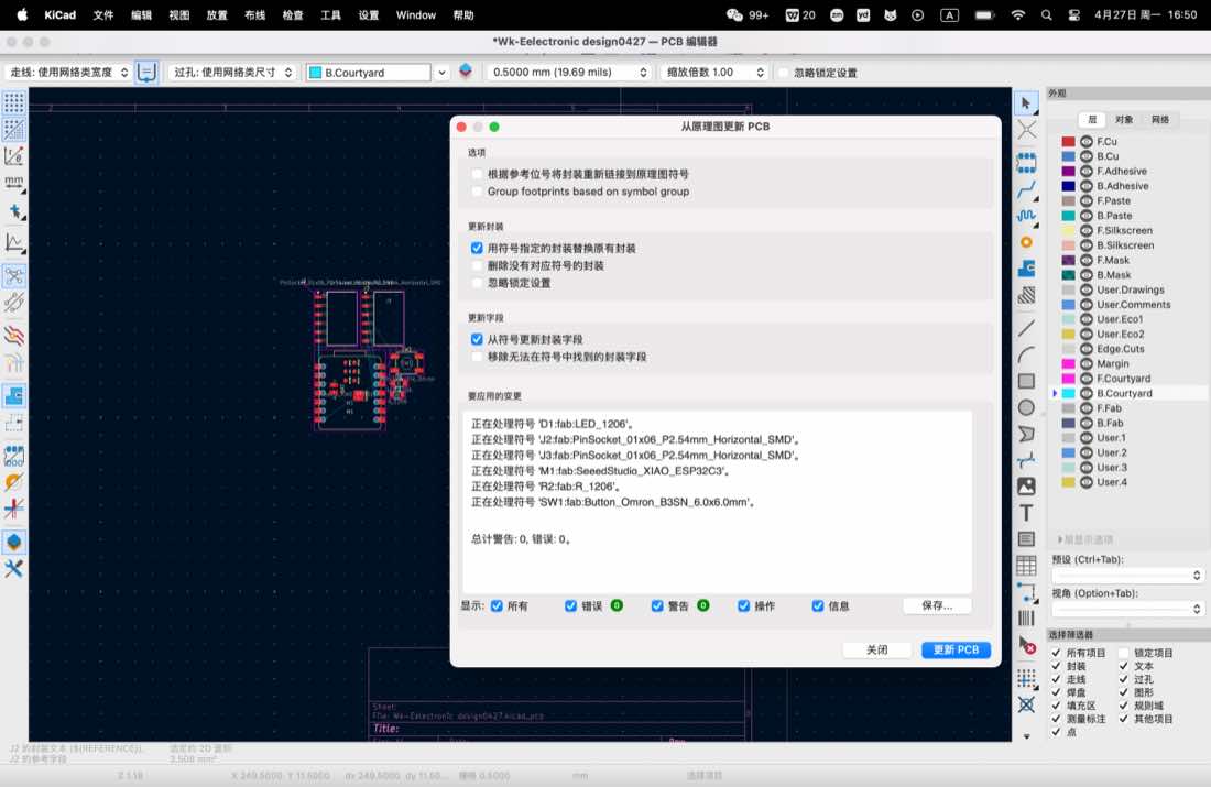
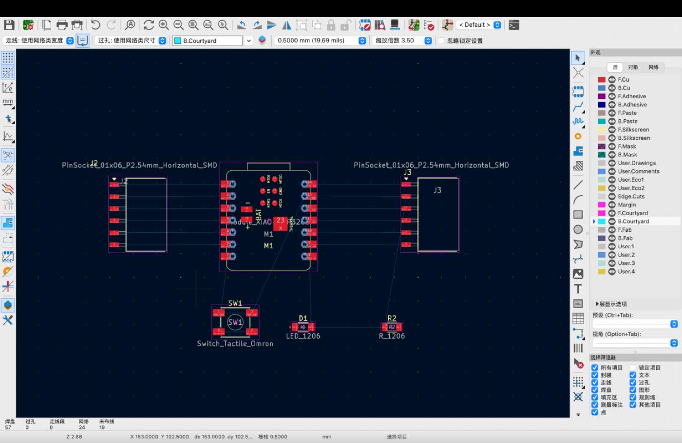
Step 4 generate the PCB diagram from the schematic
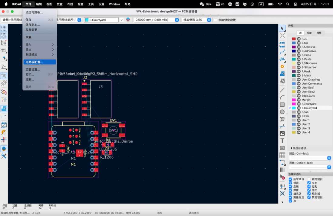
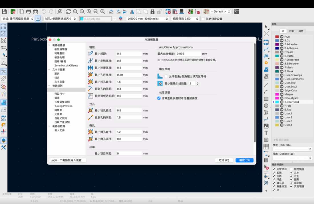
Step 5 adjuast the PCB design rule with configuration below,
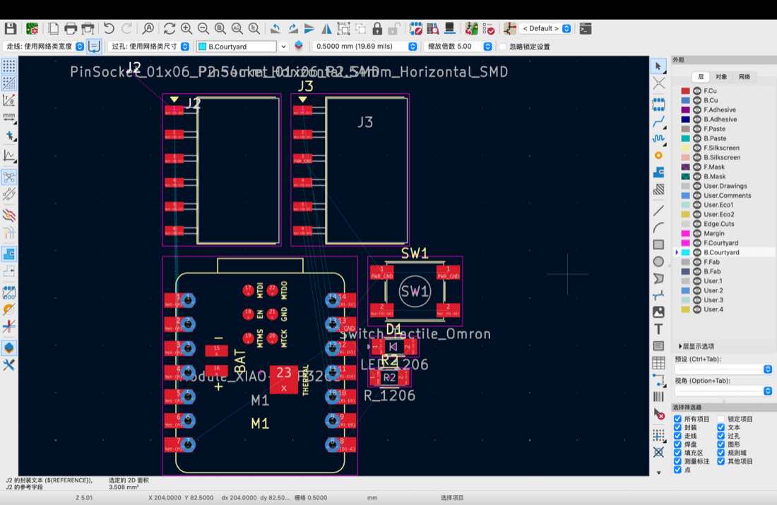
There is cable crossing issue,as below, I tried to revise the Schematic again.
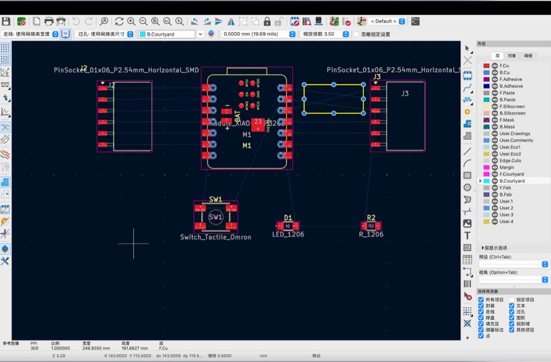
The updated schematic and PCB diagram
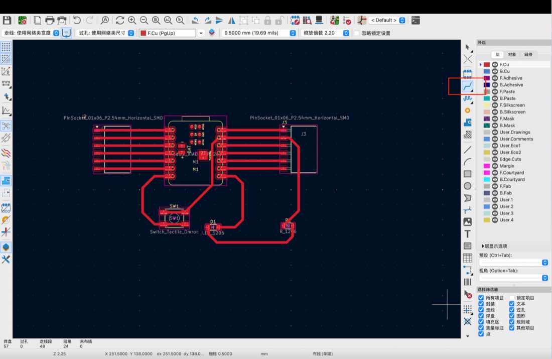
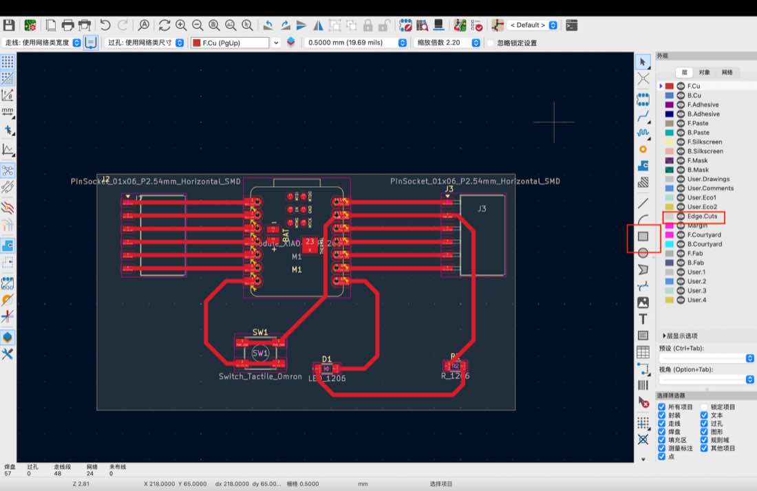
Step 6 Manual Routing by using the Route Tracks tool
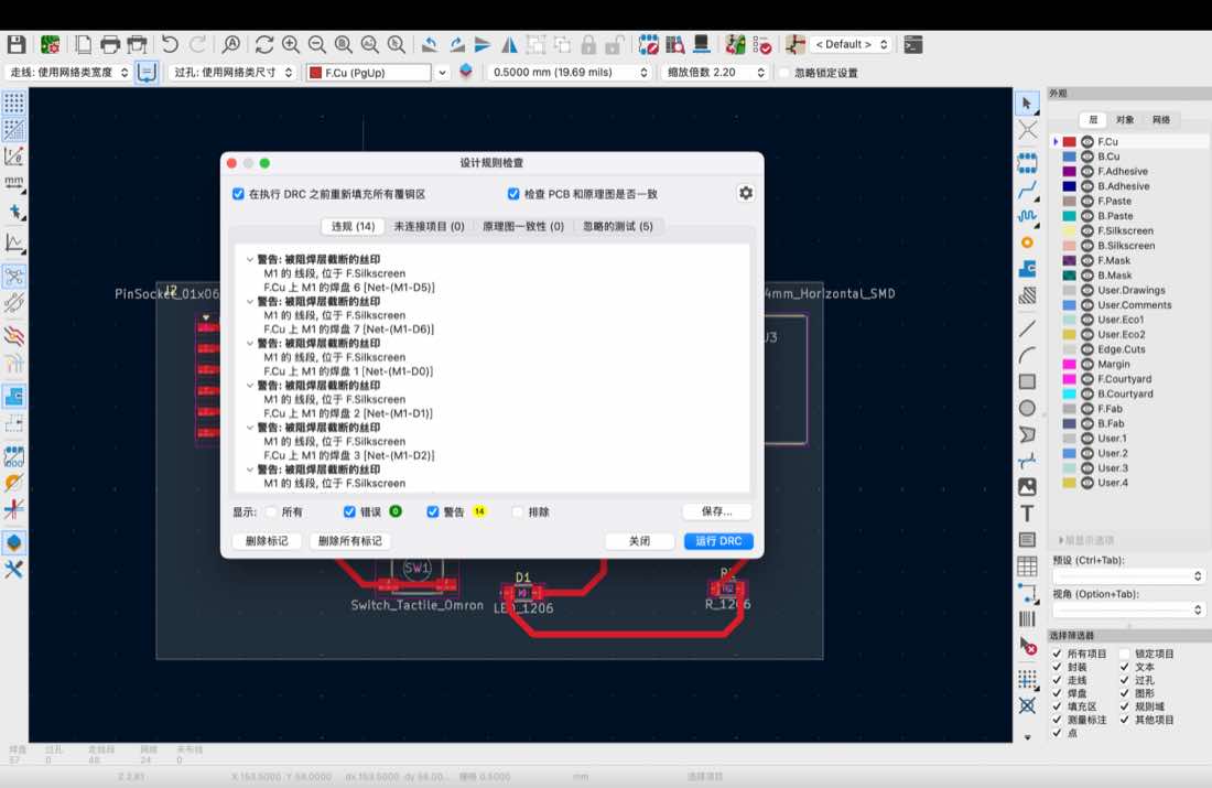
Step 7 Run DRC( Deisng rule checking )
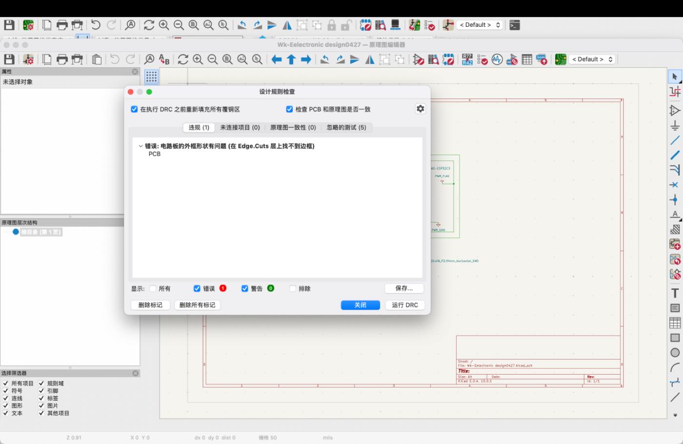
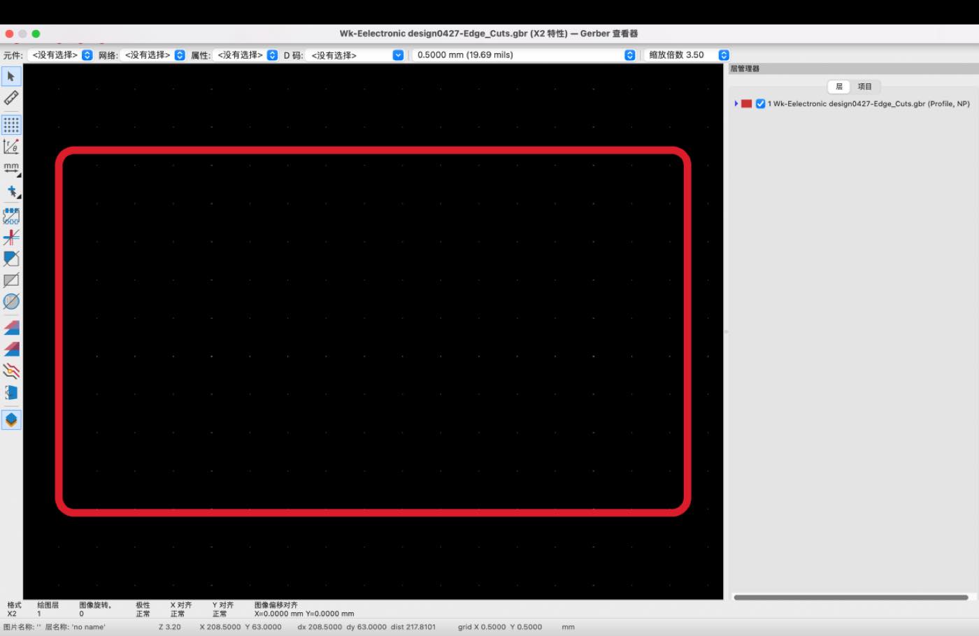
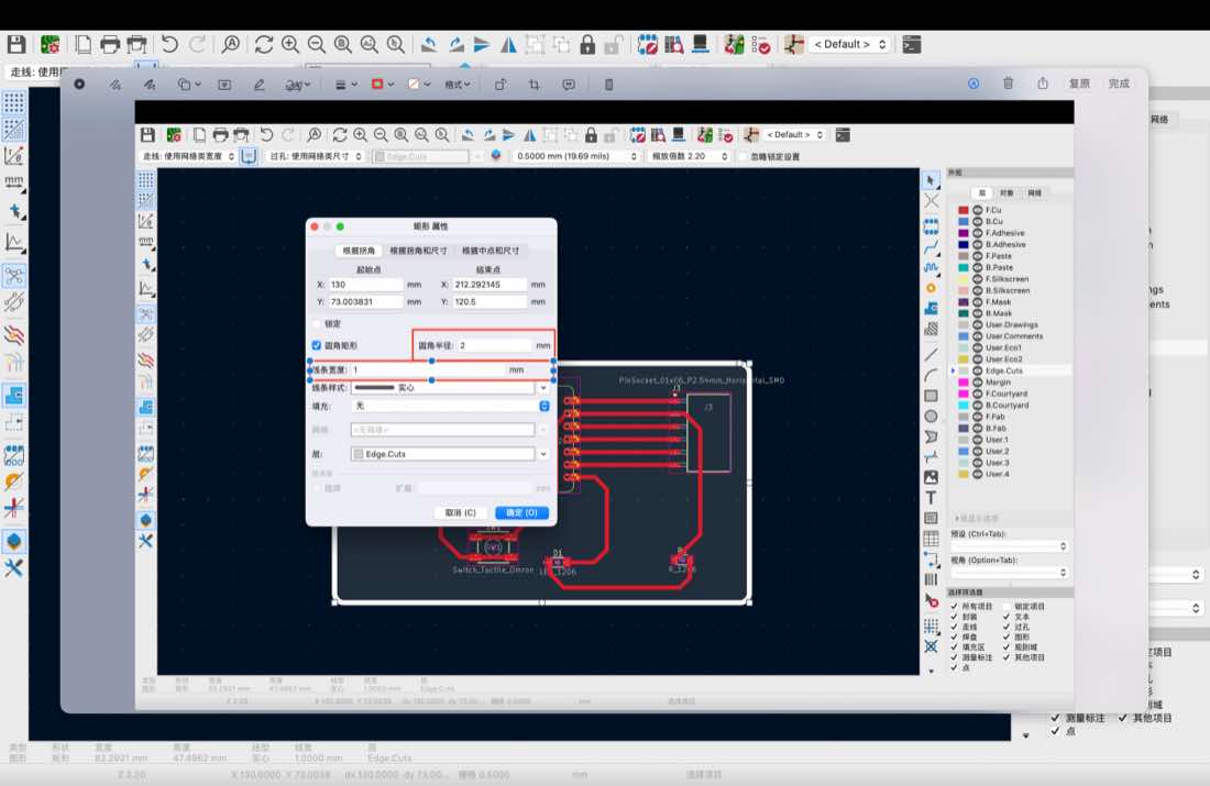
Select the Edge.cuts and then add a rectangle to contain the whole circuit and components.
Setting on the Boundary
Run DRC again, no more errors.
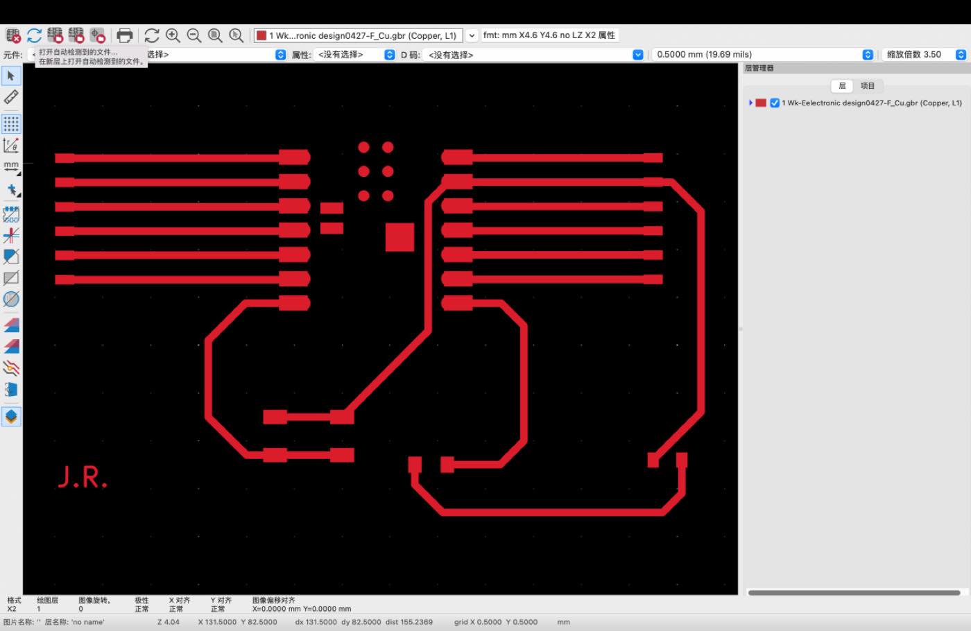
On F.cu later, add remark J.R.
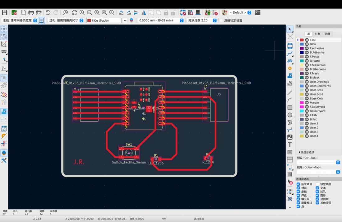
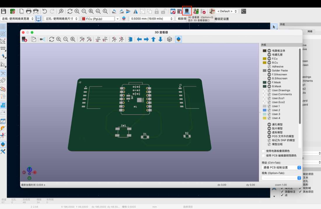
Run “3D viwer” to check the PCB
Step 8, out put the gerber file of the F.cu and edge.cuts layer.
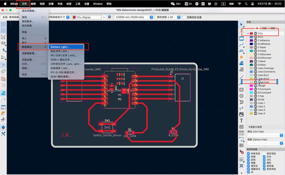
Gerbers file as attached.
Image of gerbers