Week 8
Electronics Production
Summary
In this week, the focus is on producing a physical development board using in-house PCB manufacturing techniques or external board houses. This involves toolpath generation, milling, soldering, debugging, and testing. Group activities focus on machine characterization and understanding production constraints.
Group Assignment
As part of the group assignment, we documented:
- The characterization of in-house PCB milling: feeds, speeds, depth of cut, tooling, etc.
- The workflow to prepare and send a PCB to a board house.
Individual Assignment
The individual assignment consists of fabricating and testing a microcontroller development board that I designed. Below is the detailed documentation of each step.
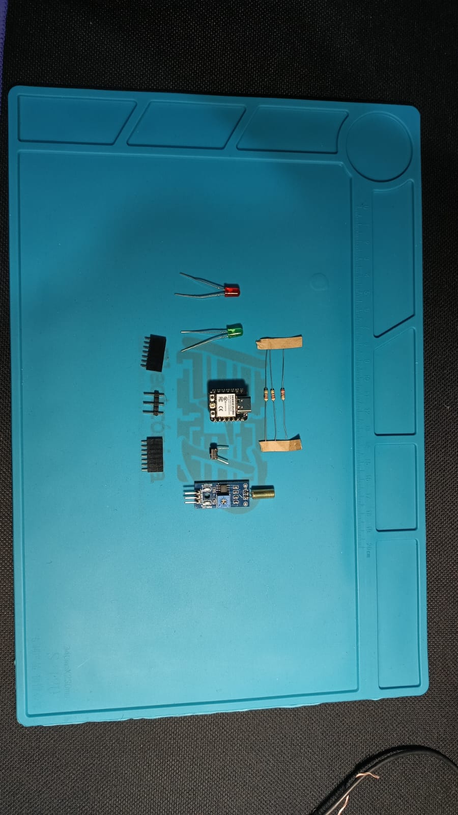
1. Component Selection and Preparation
As a first step, I gathered the necessary electronic components to build my custom development board.
| Item | Description | Function | Quantity |
|---|---|---|---|
| XIAO ESP32-C3 | Microcontroller board with built-in Wi-Fi and Bluetooth | Main control unit of the project | 1 |
| 220 Ω Resistor | Standard through-hole resistors | Used to limit current through LEDs | 3 |
| Push Button | Simple tactile momentary push button | User input | 1 |
| Male Header Pins (3-pin block) | Triple-pin male connectors (VCC, GND, Signal) | Allow external modules or sensors to be easily connected | 3 |
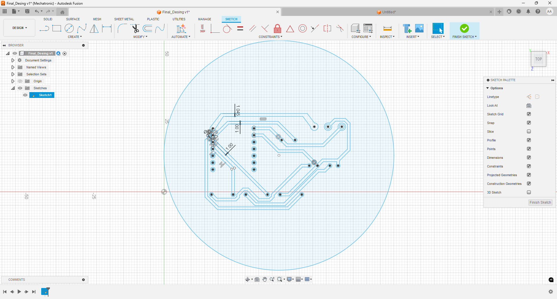
2. Importing SVG and Making Adjustments in Fusion 360
At this point, the SVG file of the board design was imported into Fusion 360 in order to make the necessary modifications. These include adjusting the track width, verifying hole dimensions, and ensuring that no routing conflicts or overlapping traces are present.
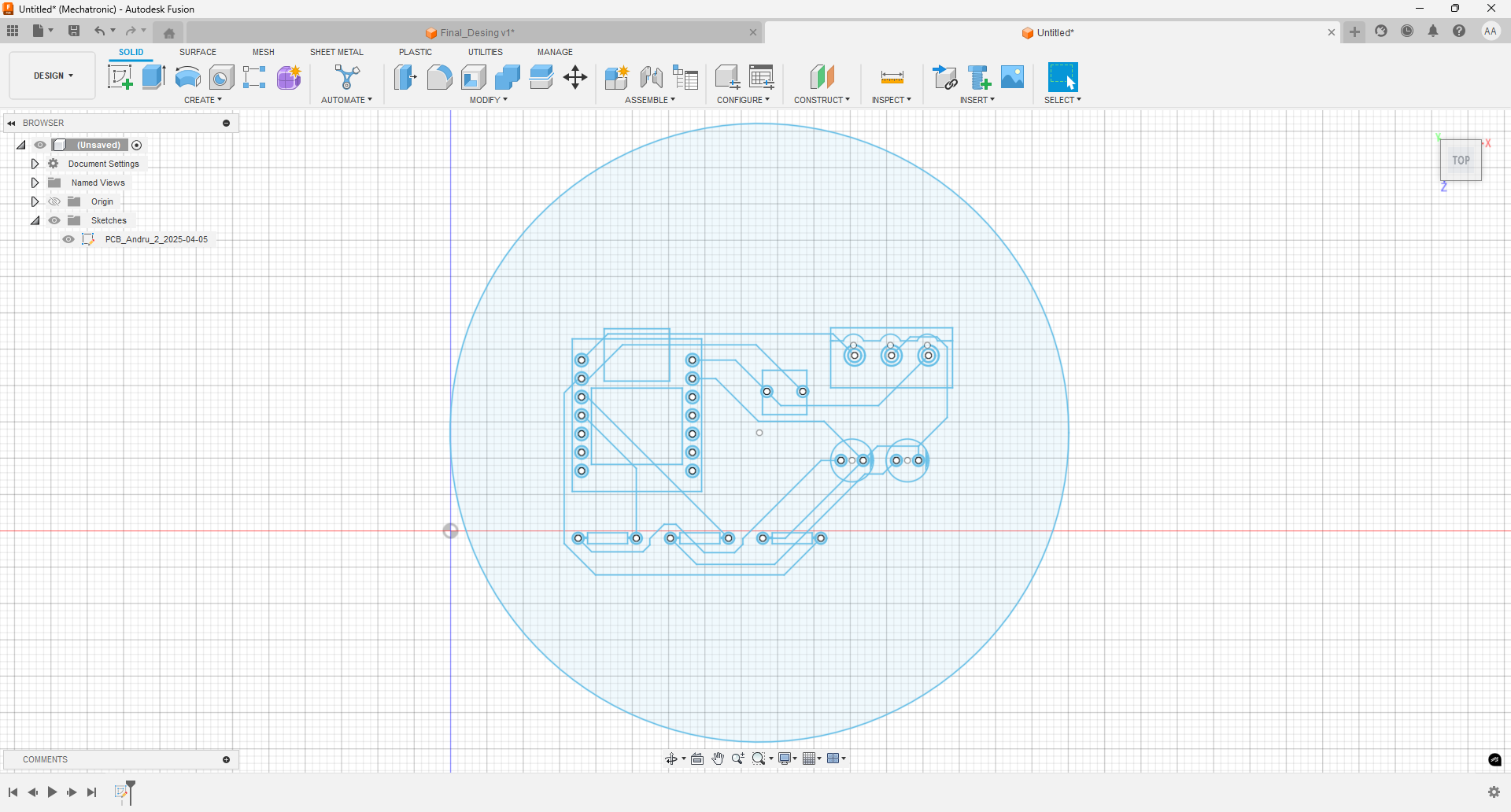
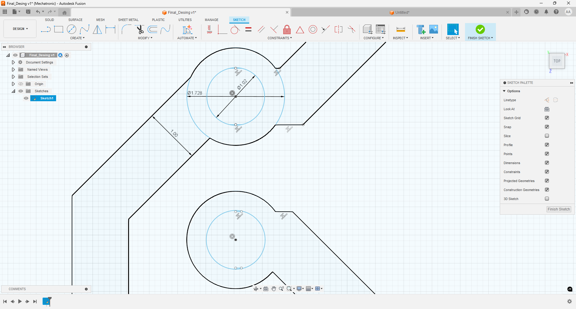
After removing the contour lines around each component and applying an offset operation to each trace with a thickness of 1 mm, I adjusted the size of the solder pads to approximately 1.728 mm in diameter. These refinements helped prepare the design for a proper toolpath and ensured the board meets the fabrication standards.
However, at first I attempted to increase the width of the traces manually in order to test whether the result would be acceptable. This approach can be useful in cases where quick manual adjustments are needed. Although the result was not as expected, I decided to keep it for comparison, so the differences could be noticed once the board was fabricated.
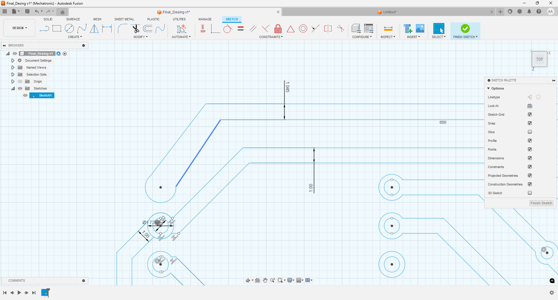
However, for the rest of the traces and solder pads, I maintained uniform measurements and verified that no traces intersected or had 90° angles. I also placed reference points at the center of each solder pad, which will later be used by the CNC machine to accurately determine where to drill.
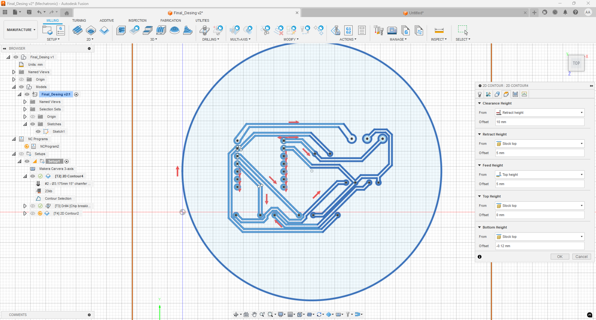
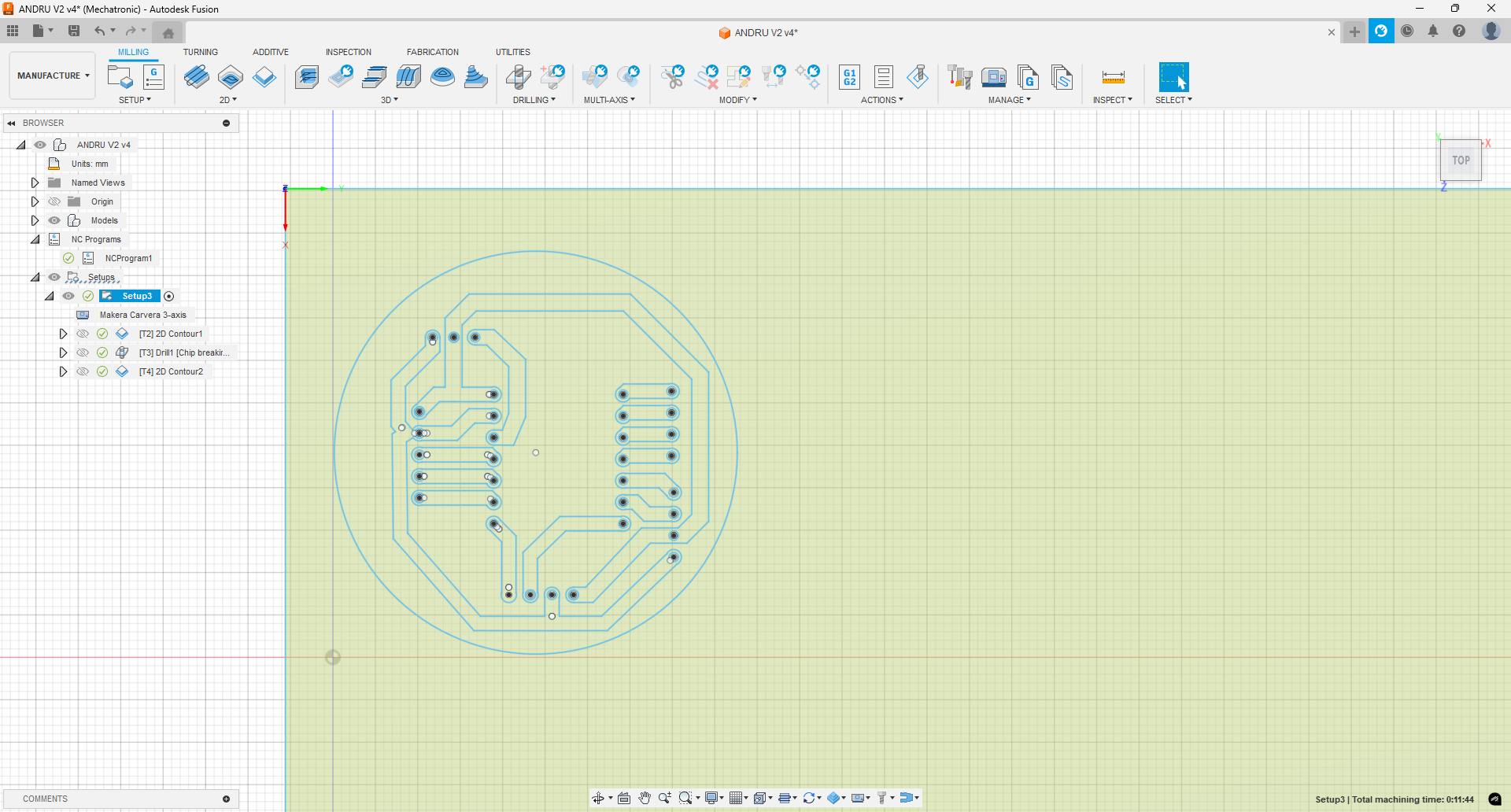
PCB Milling Setup in Fusion 360
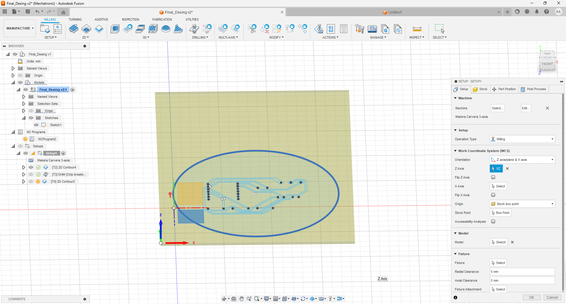
In Fusion 360, I began by selecting the Manufacture workspace to prepare the PCB milling process. I created a new setup and chose the milling machine, along with the reference axes. In my case, I selected the top corner of the lower-left edge as the origin. It’s also important to specify the dimensions of the copper boards you’re working with—in this case, I used 100 mm x 150 mm copper-clad boards.
Contour Toolpath Configuration
Then, with the support of engineer Jhonatan Cortés, I configured each of the processes involved in PCB fabrication. Each process requires a specific tool with unique characteristics, and the interaction between the tool and the material varies accordingly.
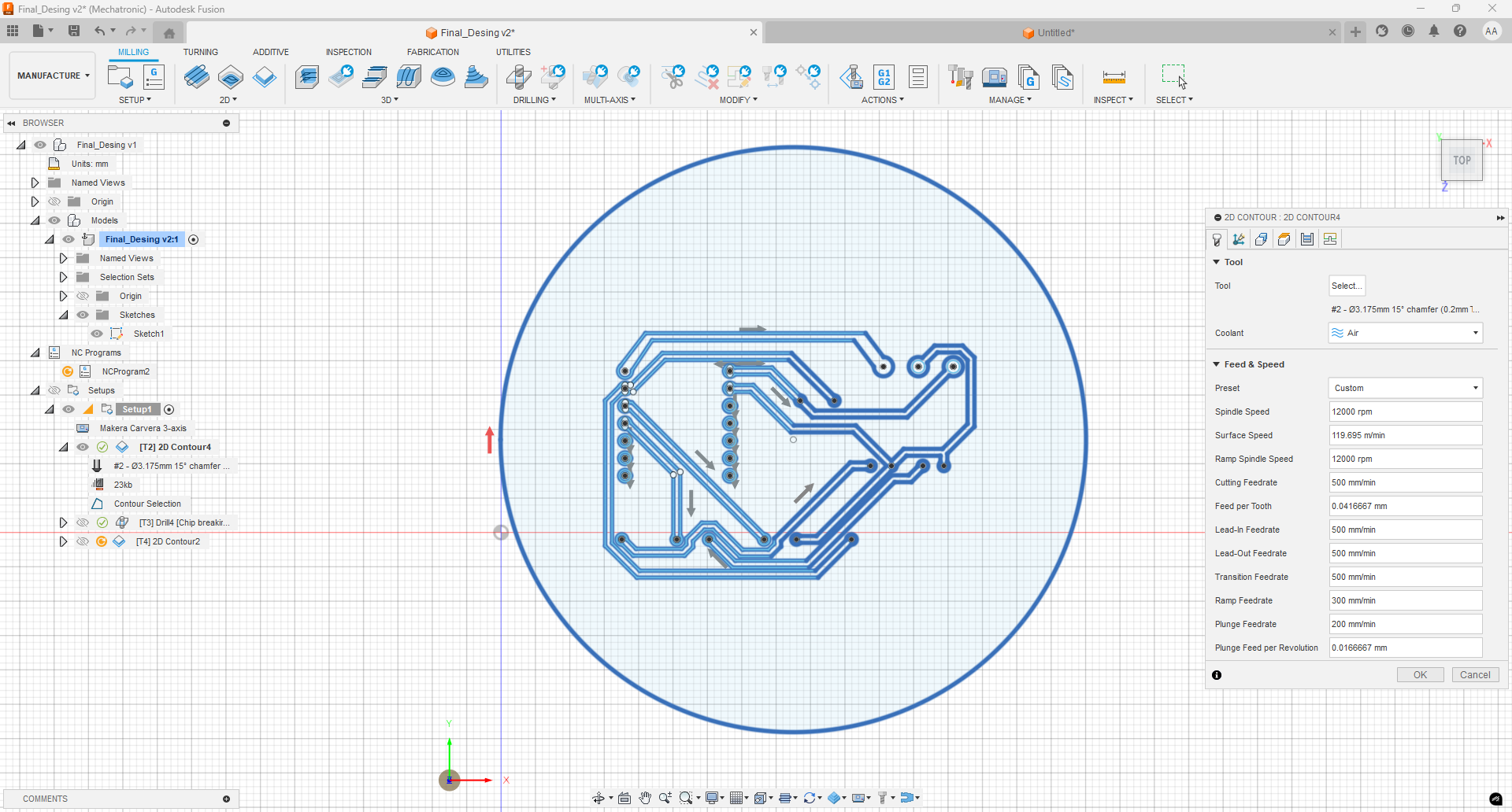
In this first case, I configured the contour milling process for the PCB traces using the Engraving/Chamfer mill tool. The selected tool had the following parameters:
- Tip diameter: 0.2 mm
- Angle: 15°
- Shaft diameter: 3.175 mm
- Tool slot: 2
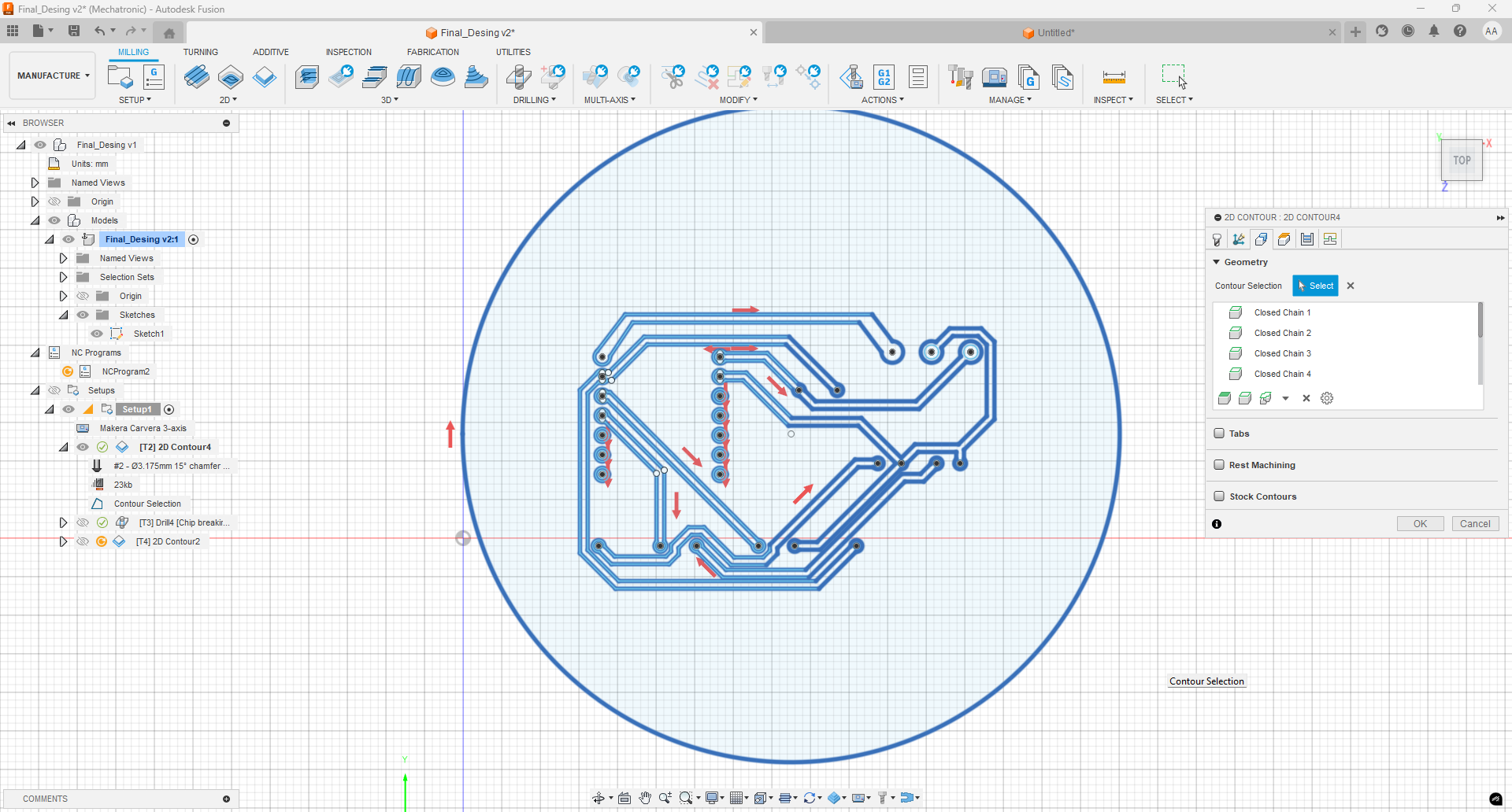
It is important to select the entire outline of the PCB traces in the Geometry section of the toolpath configuration. This ensures that the milling machine accurately follows the intended path and avoids missing any critical segments.
It is also important to define how much material will be removed from the top layer. In my case, I set a depth of -0.12 mm, which is enough to remove the copper layer but not deep enough to cut through the entire board.
Now I will present a video of the simulation of this process in Fusion 360. In this simulation, all the toolpaths can be observed, allowing me to verify that all traces are properly defined and will be correctly milled.
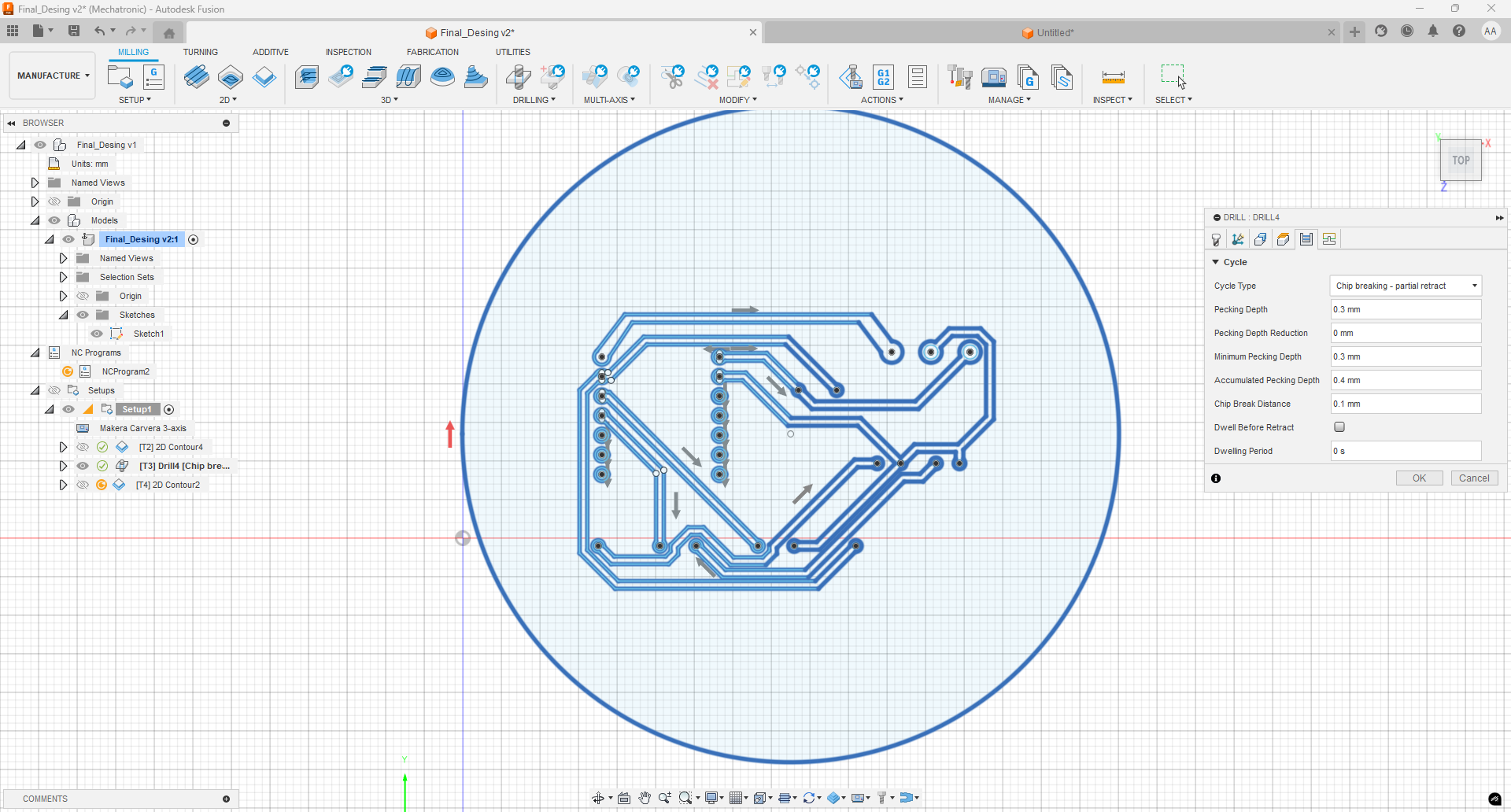
Drilling Configuration for Component Holes
Now, for the drilling process of the holes where the components will be later inserted, I used the 1 mm drill bit, located in slot 3 of the machine. Additionally, I selected the "chip breaking" cycle type. This option prevents the drill bit from overheating by retracting the tip and advancing in small increments, which is particularly important when working with materials like copper-clad boards.
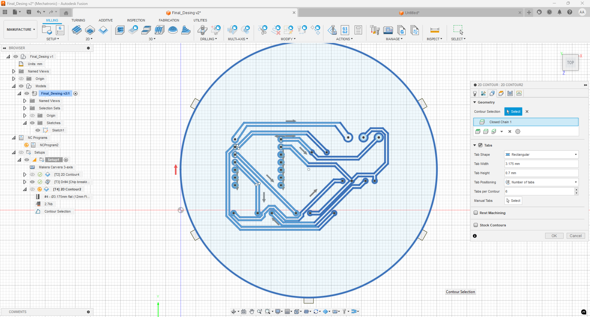
Outline Cutting of the PCB
Finally, to cut the PCB from the copper-clad board, I used the flat flute end mill tool, located in slot 4 of the milling machine. This tool has the following specifications: Diameter: 3.175 mm, Flute length: 12 mm.
In this section, it is crucial to add tabs—small support bridges that help keep the piece attached to the board during the cutting process. This significantly reduces the chance of the PCB coming loose before the operation is complete. I selected a total of six tabs strategically distributed around the perimeter of the board.
Outline Cutting Simulation
Finally, the following video shows the simulation of the PCB outline cutting stage. It clearly displays the toolpath and how the cutting process will be executed, including the support tabs that hold the board in place until the end of the operation.
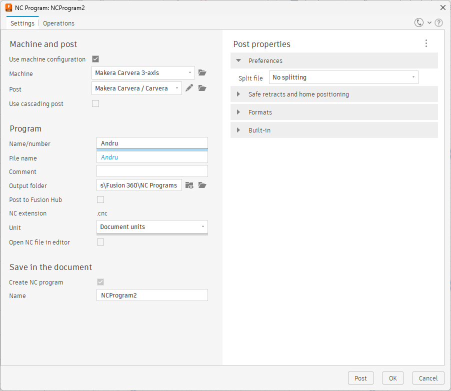
G-Code Export
Now that the toolpaths are configured, it is possible to export the G-Code so that it can be loaded into the milling machine software. To do this, right-click on the Setup item in the browser panel and select NC Program. In my case, I named the program Andru and selected the desired folder to save the exported file.
PCB Fabrication Process
Once the G-code is uploaded to the CNC machine via a WiFi connection, the fabrication process begins. Initially, the machine performs a verification routine across all tool slots to confirm the presence and height of each tool. It is important to note that the machine does not validate if the correct tool type is placed—this must be ensured manually prior to starting the job.
The video below shows the moment when the machine selects the drilling tool to begin creating the holes. The earlier tool calibration steps and other initial routines were recorded in vertical format, so only this horizontal-format video is included as recommended for documentation purposes.
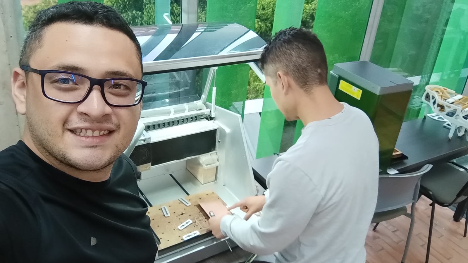
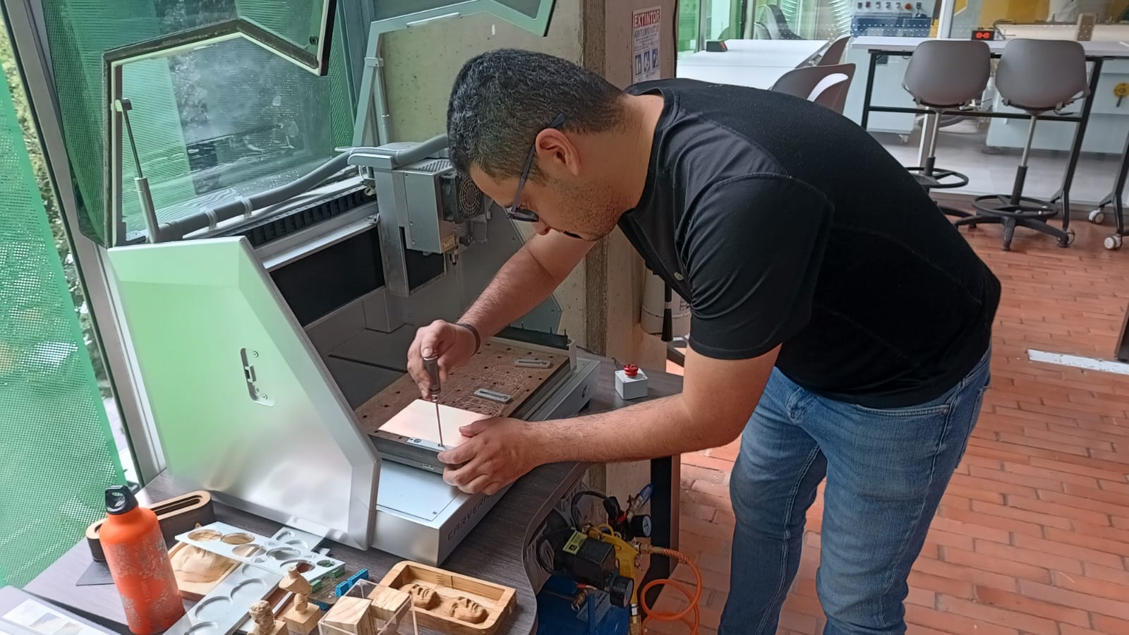
Here is a photo with Engineer Jhonatan, who works at the Fab Lab and is responsible for operating all the machines and handling institutional design requests at the university.
Continuing with the fabrication process, in the following video the CNC machine begins cutting the PCB from the copper-clad board. Spoiler: just seconds before the accident. The tool starts descending slowly in a ramping motion, which had been configured to avoid direct vertical entry into the board, reducing the chances of tool breakage.
As previously mentioned, the tool broke during the initial cutting process. This made it necessary to return to Fusion 360 and leave only the PCB cutting stage in the workflow. A new G-Code was generated and sent again to the CNC machine.
The issue was caused by a high feed rate configuration, which made the tool advance too quickly. This excessive speed generated too much friction between the copper board and the tool, ultimately leading to breakage.
Finally, once the issue was resolved, the machine successfully completed the PCB cut. The tabs that had been previously configured in Fusion 360 were respected during the milling process, keeping the board attached to the material base until the very end.
The following video shows the cutting process at 6x speed to clearly demonstrate how the final contouring was completed without issues.
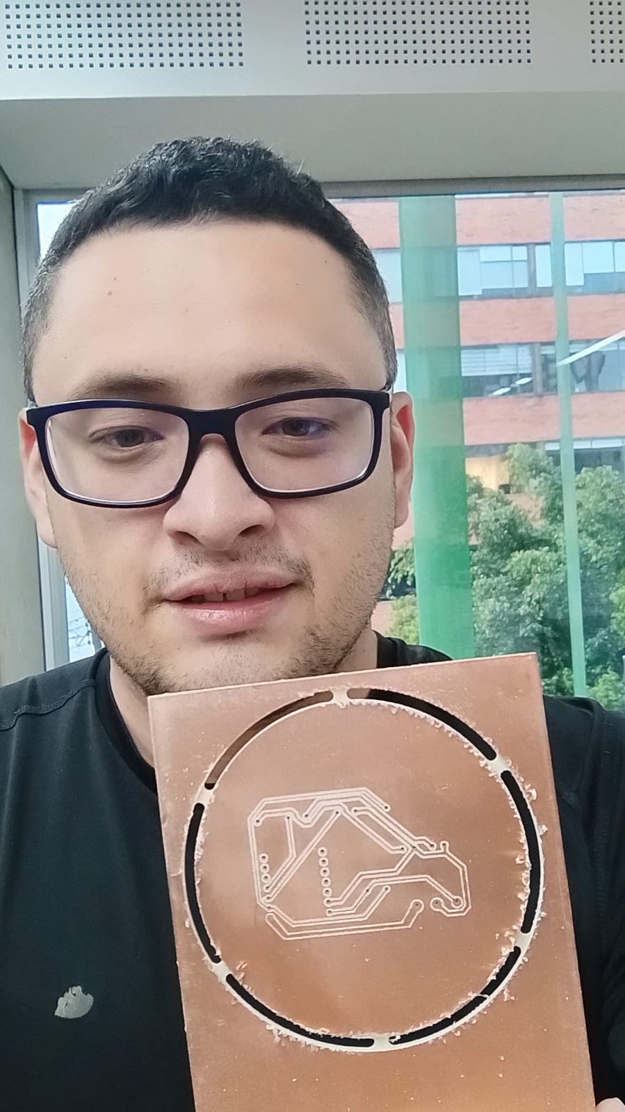
Here you can see a photo in vertical format 😢 of the final result of the PCB.
Soldering the Components
Now, in the soldering process — with both the components and the fabricated PCB ready — the goal is to assemble a functional and practical development board.
Testing and Validation
During the assembly process, I encountered several issues that complicated the soldering. The main problem was that the PCB traces were too thin, which caused the solder to easily bridge across adjacent tracks. Additionally, since I had configured both the solder mask and the components to be on the top layer, the soldering process became even more difficult, making it challenging to achieve clean and reliable joints.
😔 Unfortunately, this PCB did not fulfill its intended functionality and cannot be used in its current state. Therefore, it was necessary to start the entire process from scratch. However, this experience provided valuable lessons:
- It is essential to increase the width of the traces to make the soldering process easier and safer.
- It is necessary to increase the clearance between traces to avoid unwanted shorts.
- It is important to either apply the mirror tool to flip the design so that the components are mounted on the opposite side of the copper layer or work directly on the bottom layer without needing to manually invert the microcontroller terminals.
New PCB Design
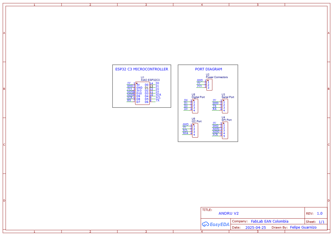
After reflecting on the issues encountered in the first fabrication attempt, I decided to completely redesign the board. In this new version, I chose not to directly integrate components onto the PCB itself. Instead, I strategically expanded the microcontroller’s ports to make future connections easier and more modular.
I allocated three dedicated pins for 3.3V, 5V, and GND outputs. Additionally, I created a 4-pin header for D0 through D3 digital I/O connections, a 4-pin header for GND, 5V, SCL, and SDA lines for I2C communication, another 4-pin header for 5V, GND, TX, and RX for serial communication, and finally, a 5-pin header for 5V, GND, MOSI, MISO, and SCK to support SPI communication.
In Fusion 360, I carefully adjusted the entire track layout, ensuring proper trace thickness, spacing, and correcting broken or incomplete connections that occasionally appeared after initial routing. This optimization was crucial to improve manufacturability and the reliability of the final PCB.
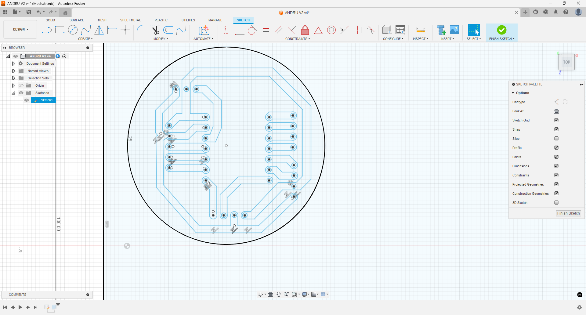
In the manufacturing workspace, I had to reprogram the operations for track contouring, drilling, and final PCB outline cutting. Once everything was properly configured, I exported the updated G-code for the machine to fabricate the new board.
Now I prepared another board to be able to send the G-code and generate my new PCB.
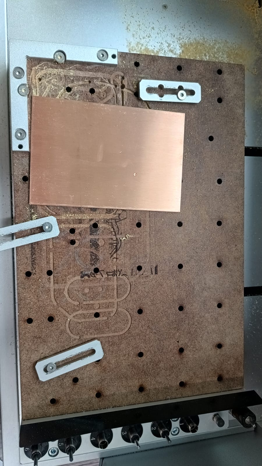
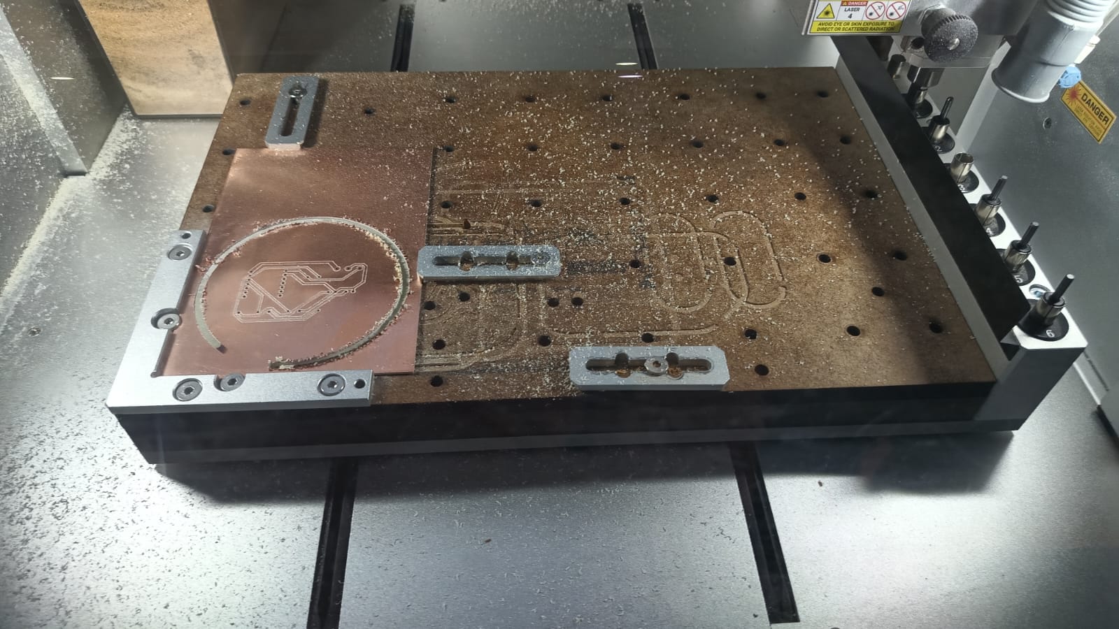
I secured the copper board onto the CNC working bed using screws and mechanical stoppers to ensure that the board would remain perfectly fixed during the different stages of the milling process. This way, any potential displacements during the tool changes or cutting operations would be avoided, guaranteeing a more precise and reliable result.
In this stage, the machine is performing the drilling process to create the component holes on the PCB. Accurate hole placement is essential to ensure that all components can later be inserted and soldered correctly without alignment issues.
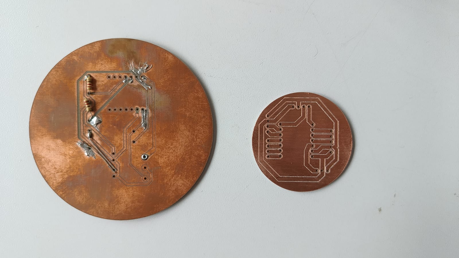
A significant improvement can be observed between the final results. I managed to significantly reduce the PCB size, which improves material efficiency. Additionally, the traces are thicker and the overall layout is much more organized compared to the first test.
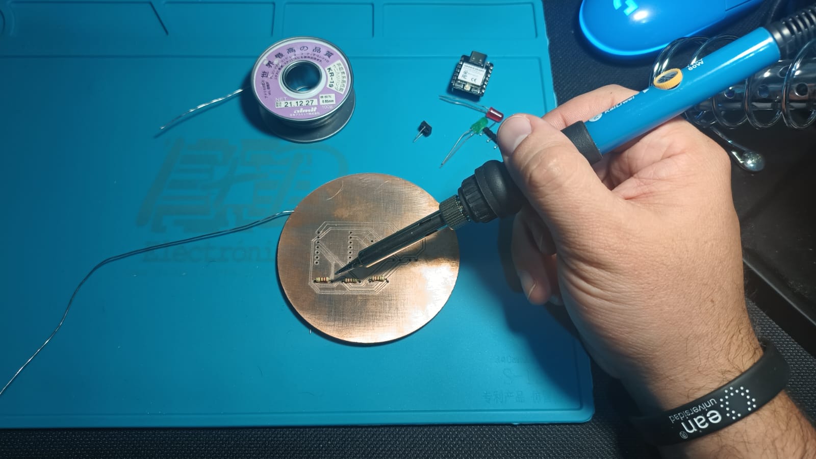
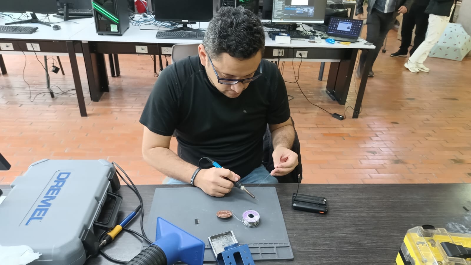
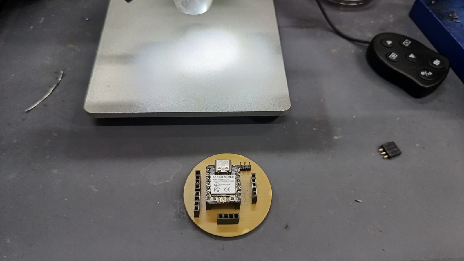
I started the soldering process by carefully placing the components onto the newly fabricated PCB. This time, the layout was much more organized, and the larger traces made the soldering process significantly easier and cleaner.
Soldering Process
For assembling the PCB, I used the traditional through-hole soldering technique. The image below shows the tools and materials used during the process: a temperature-controlled soldering iron, high-quality solder wire (0.7 mm diameter), and the freshly milled copper PCB. The PCB was carefully placed on a heat-resistant silicone mat to prevent accidental damage to the work surface and to help dissipate heat during soldering.
Each component was placed on the board and soldered individually. I applied the soldering iron tip to the pad and lead, then fed in the solder wire to create clean and reliable joints. The process required steady hands and attention to detail, especially to avoid bridging pads or leaving cold joints. The result was a board with robust electrical connections, ready for programming and testing.
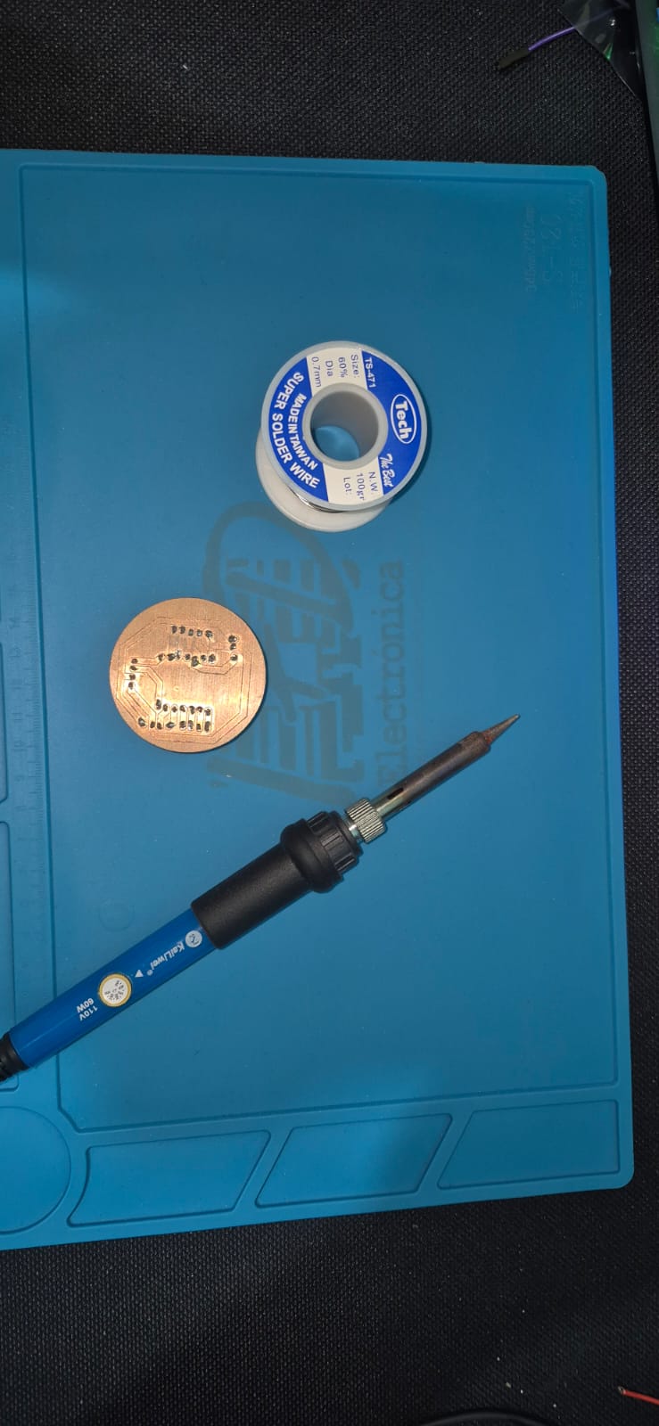
Tools and materials used for the soldering process: soldering iron, solder wire, and the milled PCB on a silicone mat.
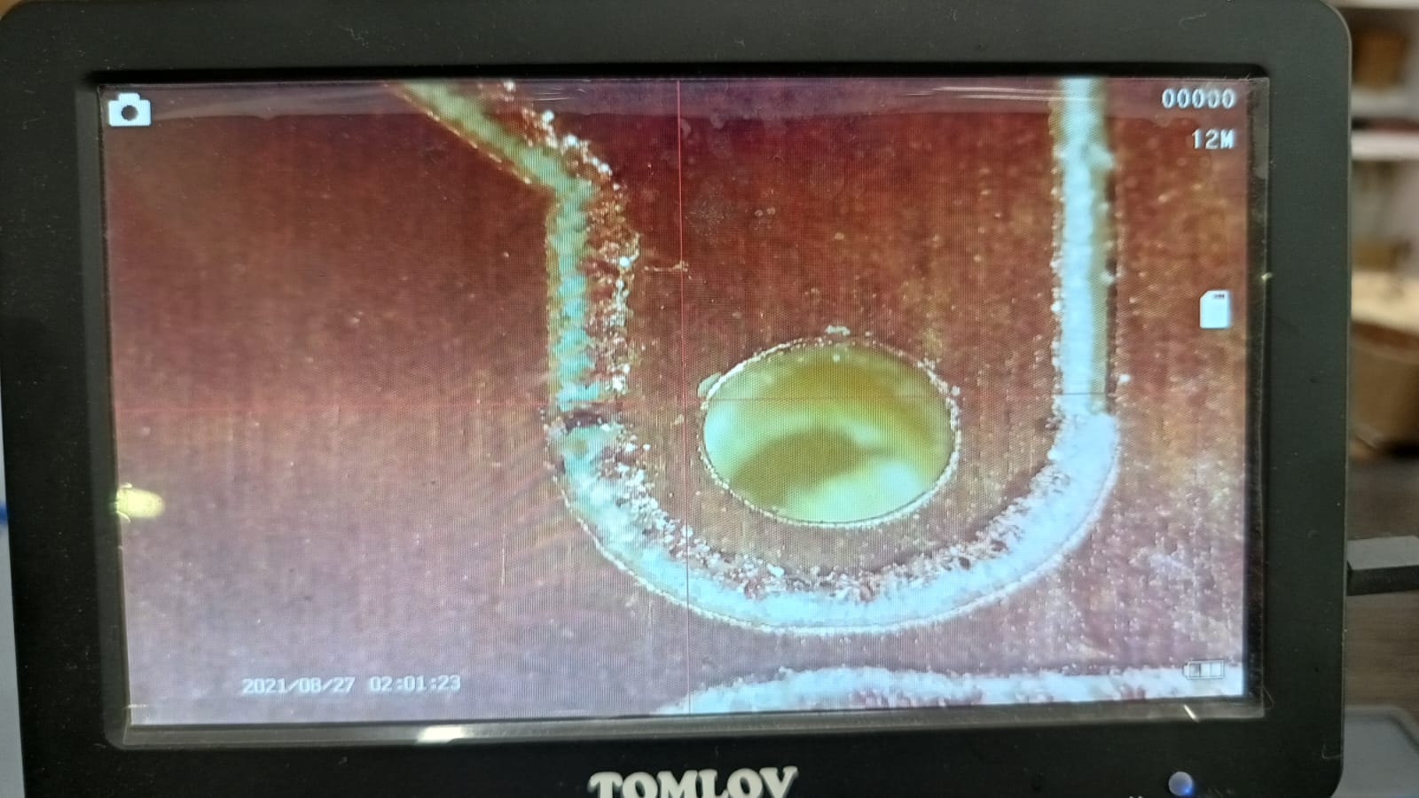
During the soldering process, I continuously checked the continuity to ensure there were no unwanted connections. At one point, I detected continuity between a trace and an unrelated part of the PCB. After carefully inspecting under a microscope and confirming that the issue was not at the soldering point, I decided to trace the path along the PCB. I discovered that a small piece of copper had accidentally remained, creating an unintended connection between the two areas.
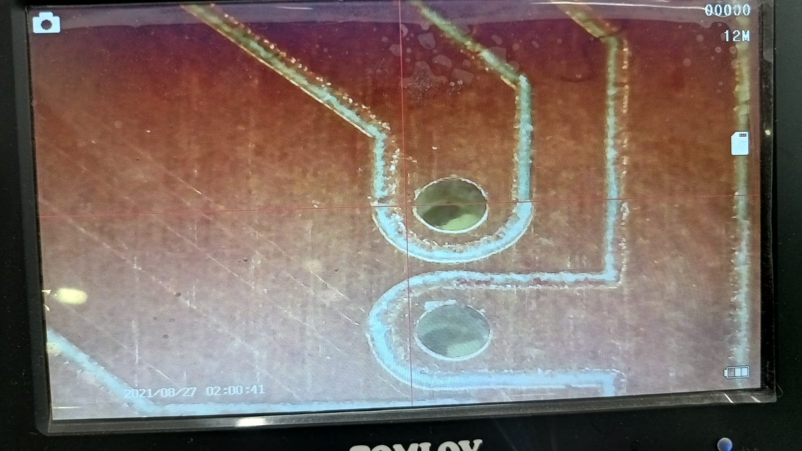
Probably it would have taken me much longer to detect the problem if I had not used the microscope. After thoroughly inspecting the PCB, I decided to cut the small unintended copper bridge using a precision knife (scalpel), thus restoring the electrical isolation between the tracks.
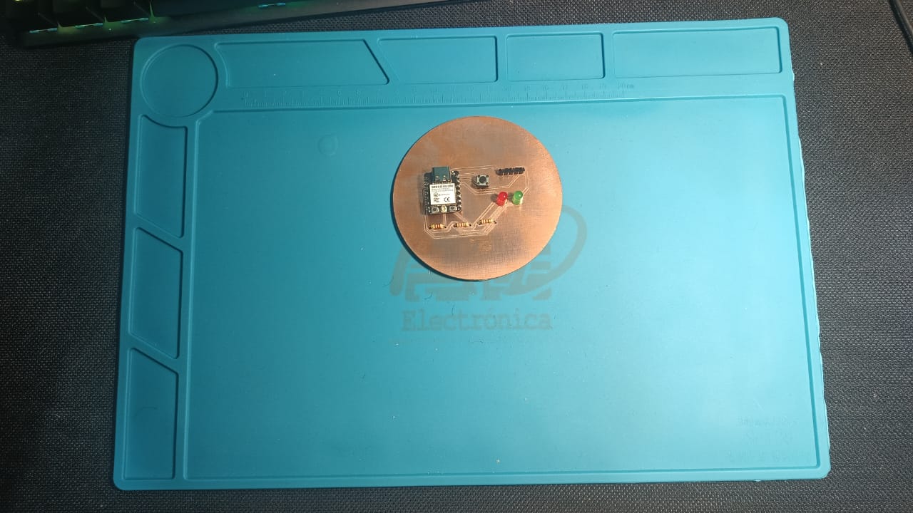
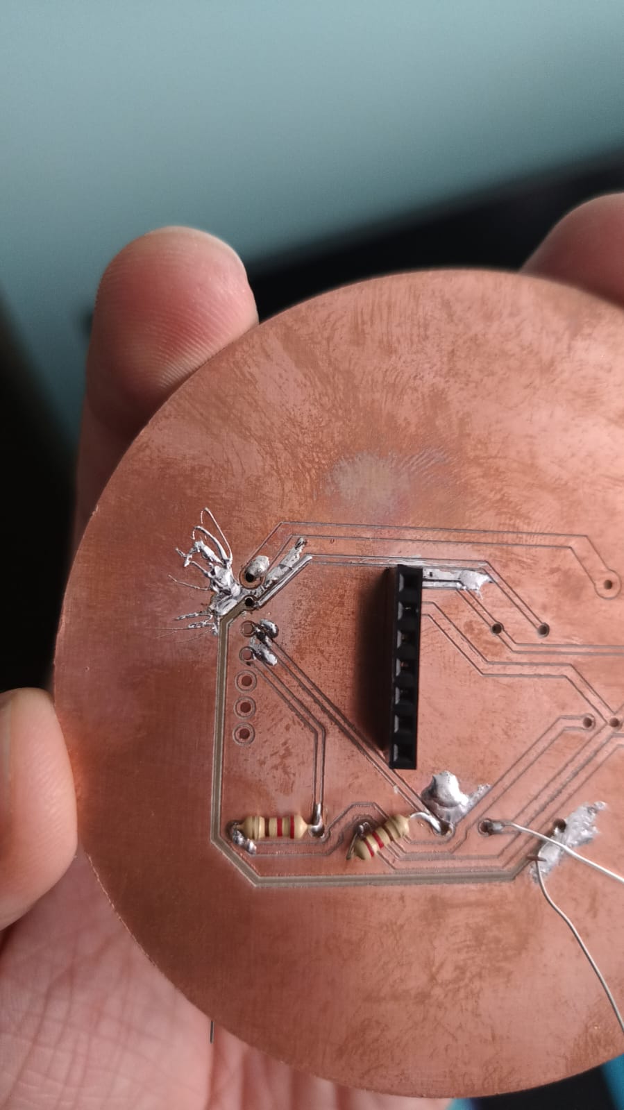
Once I finished soldering all the components onto the new PCB, I achieved the following result. The improved organization of the tracks and the compact design made the final board much more professional and reliable compared to the initial attempt.
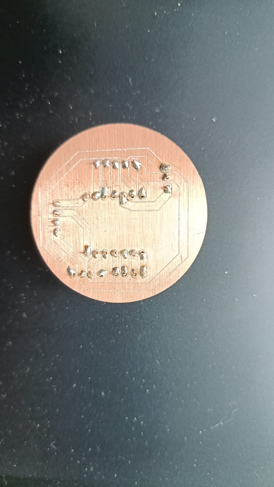
The following image shows the top layer of the PCB and the state of each solder joint. At this stage, I realized that it would be better to use a smaller drill bit when creating the holes. This adjustment would reduce the distance between the connection pins and the copper tracks, minimizing the need for the solder to flow extensively to establish proper contact.
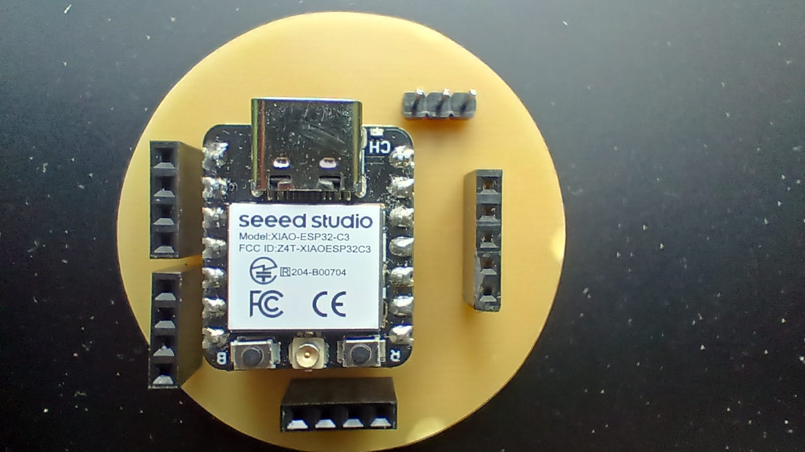
Finally, the final result of the PCB construction can be appreciated. After the adjustments made in the second attempt, the outcome shows significant improvements in track thickness, spacing, and general organization, resulting in a cleaner and more functional board ready for further testing and integration.
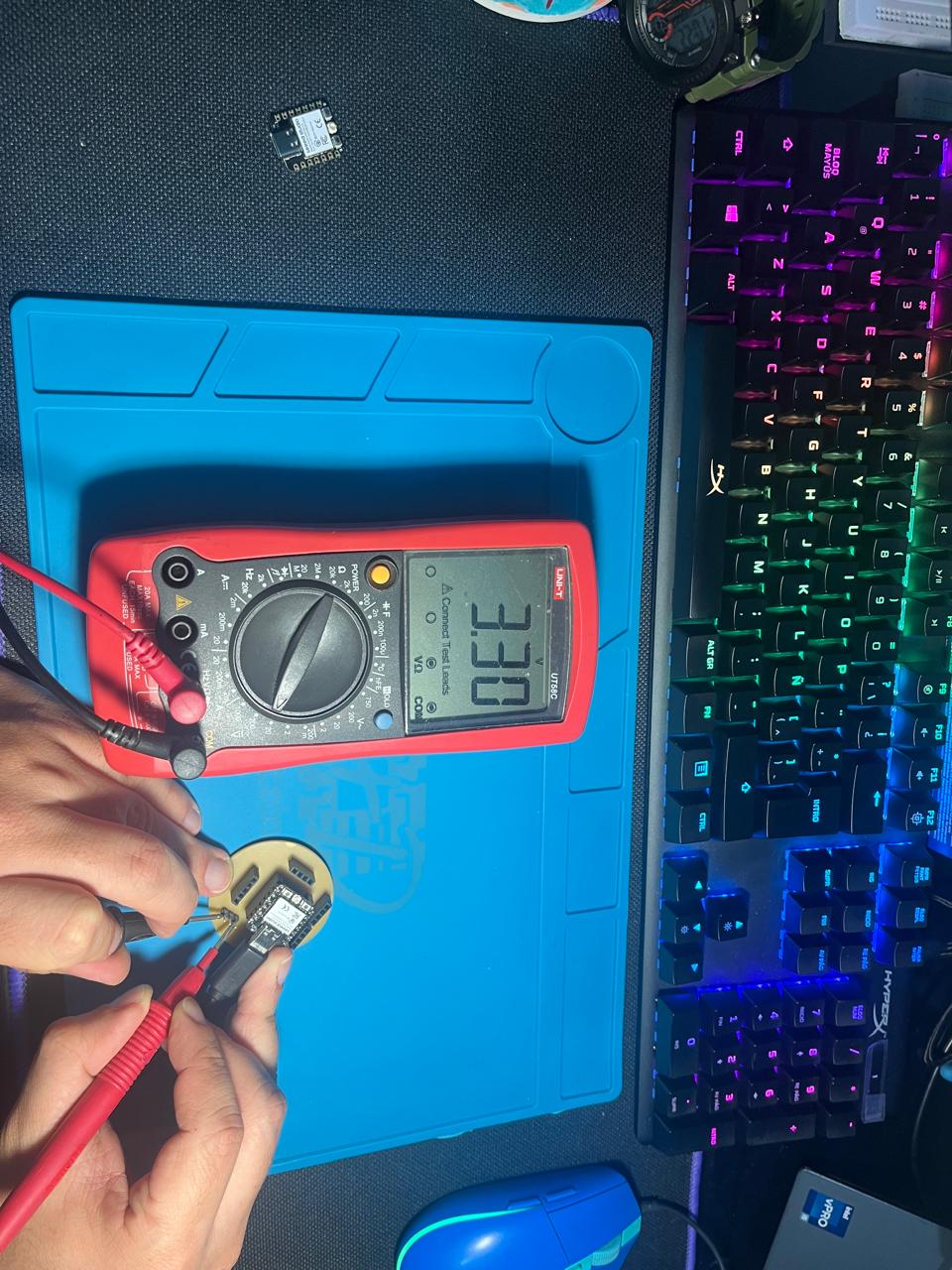
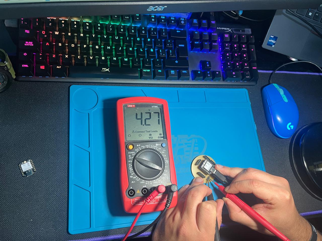
Now, to verify that there were no shorts and that the board was correctly connected, I decided to measure the 3.3V and 5V voltages present at the pins I allocated to share power with input and output devices that I will use in the following weeks.
Programming and Debugging: Blink Test on XIAO
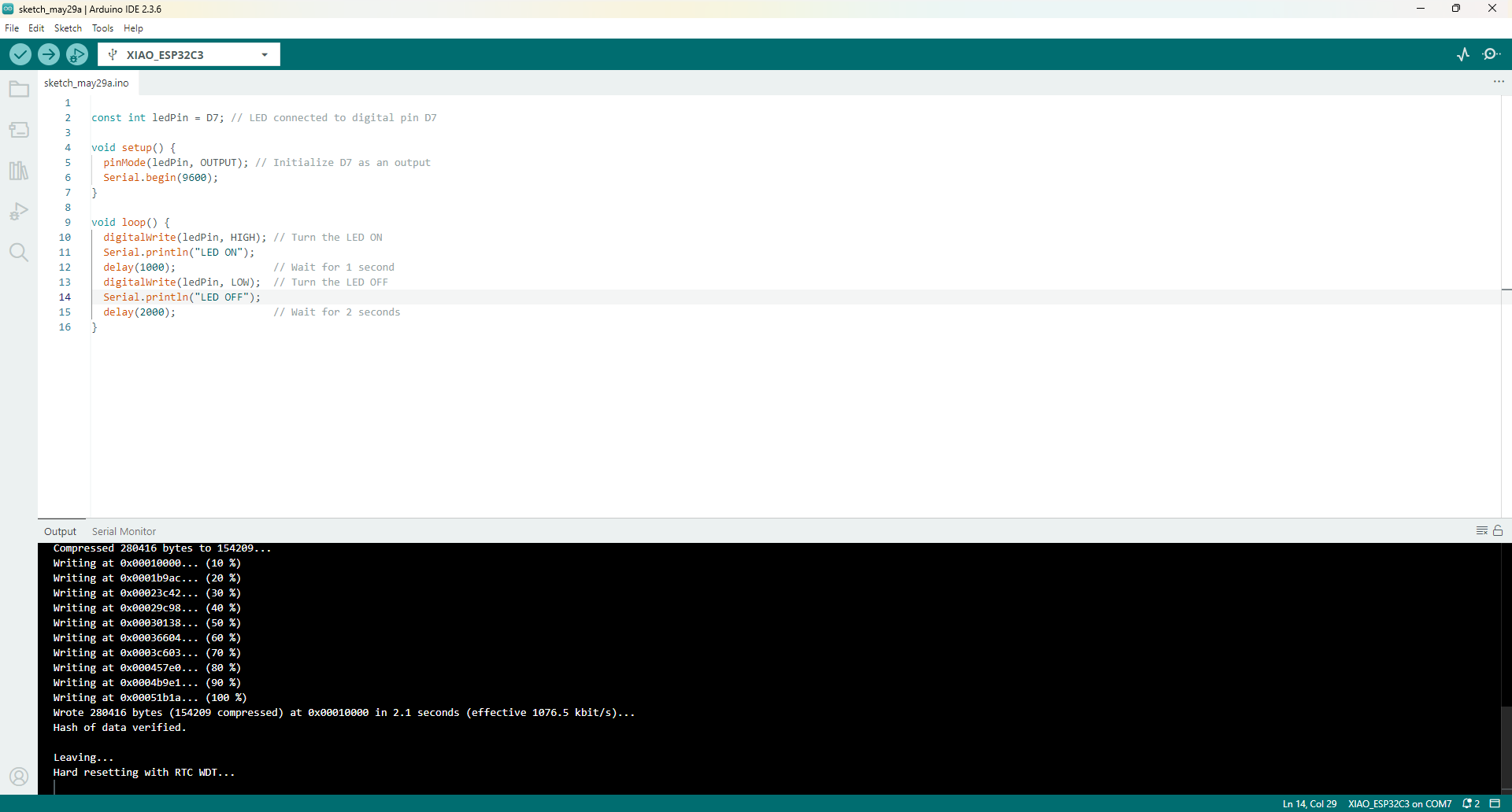
The image above shows the Arduino IDE with the code used to blink an LED connected to pin D7 on the XIAO ESP32-C3. The program turns the LED on for one second and off for two seconds, creating a visible blink every three seconds. Serial messages are also printed to the monitor to confirm the board’s operation.
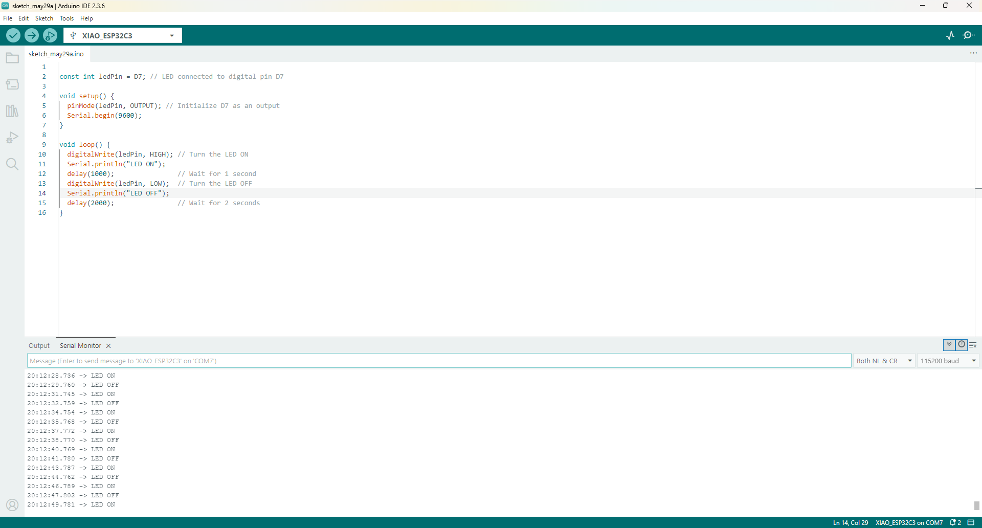
The screenshot above shows the successful upload of the code to the XIAO ESP32-C3 and the serial monitor output. Each cycle, the board prints "LED ON" and "LED OFF" messages, confirming the program is running correctly and the LED is blinking as expected.
Video demonstration: The LED connected to pin D7 blinks every three seconds, matching the programmed timing in the Arduino sketch.
Reflections and Conclusions
At the second attempt at designing and producing my PCB taught me valuable lessons. I realized that proper track thickness, sufficient spacing, and careful layer management are crucial for achieving a functional and reliable board.
During the fabrication and soldering process, using additional tools like the microscope allowed me to detect and solve hidden connectivity issues that could have compromised the operation of the final device. Being able to identify and remove a small unwanted copper bridge with a scalpel was critical to saving the board.
Another important takeaway is that optimizing the PCB layout not only improves functionality but also material efficiency. Reducing the board's footprint and maintaining organized routing significantly facilitated the assembly and inspection phases.
Overall, this experience highlighted the importance of iterative design, the value of paying attention to fine details, and how proactive verification at every stage can prevent major problems later. I now feel more confident to apply these improvements in future projects that require custom PCB design and production.
Downloads and Deliverables
Below are the downloadable resources related to the PCB development process, including both the initial and final designs. These files can be reviewed for understanding the evolution of the project and the improvements made throughout the assignment.