This week's assignment was:
- Use the test equipment in your lab to observe the operation of a microcontroller circuit board
- Send a PCB out to a board house
- Use an EDA tool to design a development board to interact and communicate with an embedded microcontroller, produce it, and test it
- Extra credit: try another design workflow
- Extra credit: design a case for it
- Extra credit: simulate its operation
ORGANIZATION
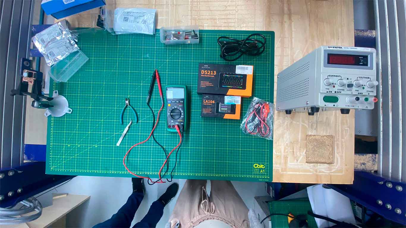
In the FAB LAB UCSUR we find all the tools to carry out the group assignment. Together with my colleague Maryori we supported each other to carry out and here I also show how I organized myself for this week.
| Wednesday 13th: | Fab Academy classes, organization for the week and preparing the materials and tools for the group assignment. |
|---|---|
| Thursday 14th: | First group progress, use of tools for the group assignment, investigation of their use, progress of the assignment and first commit. |
| Friday 15th: | Finish the group assignment, develop my board design, check and research electronic design and learn KICAD. |
| Saturday 16th: | Enter OPEN GLOBAL TIME, learn more about KICAD, develop my board, mill my board and solder components. |
| Sunday: 17th: | Carry out documentation of everything developed. |
| Monday 18th: | Carry out 3D case design for the board, LED and OUTPUTS programming. Make a 3rd commit. |
| Tuesday 19th: | Review and analyze some problems with the assignment. Print case in 3D, program LED and make the last commit of the assignment. |
GROUP ASSIGNMENT
Here I leave the link to go to the group assignments page.
Clic here to visit the WEEK 8 GROUP ASSIGNMENT PAGE
TEST EQUIPMENT
FAB LAB UCSUR IMPLEMENTS
In the FAB LAB UCSUR we have the following components to be able to carry out the following group assignment: MULTIMETER, LOGIC ANALYZER, MINI OSCILLOSCOPE and DC VOLTAGE SUPPLY. In the next section I will explain how we performed the test with all these instruments at QUENTORRES.
TESTING WITH MULTIMETER
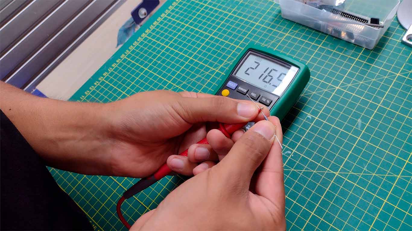
To understand the use of the multimeter, we will first test the components alone and then apply it to the QUENTORRES board developed in week 4 of ELECTRONIC PRODUCTION. First we will start to see the polarity of 2 types of LEDS, the first will be the DIP LED and then the SMD LED .
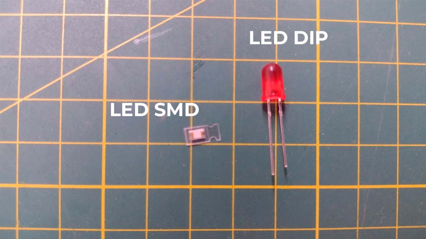
What we have to take into account is knowing which of the poles of each LED is negative or positive. In the DIP LED, the negative is always the one that is shorter and the other is positive. On the other hand, in the SMD LED, there is a green mark that the component has, the side where it is located on the LED is the negative pole and the other is the positive pole.
On the multimeter, we have to choose the "DIODE TEST" option that has the logo marked in the photograph. This will help us see if the LEDs are working correctly.
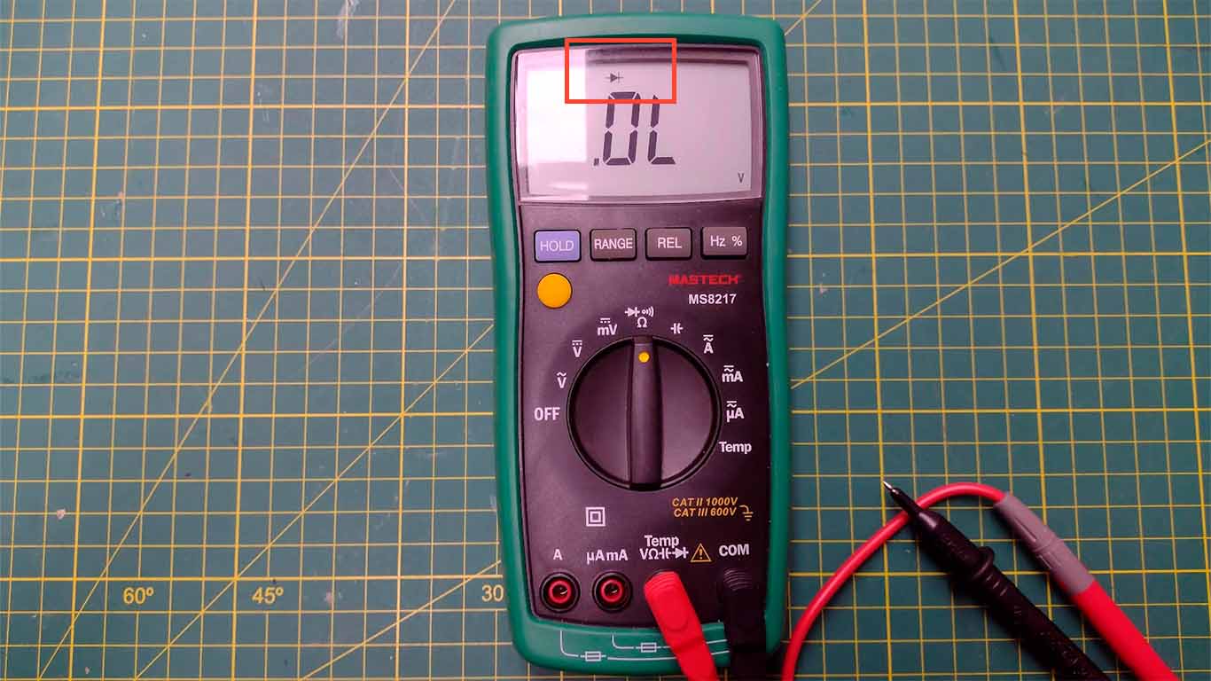
Here is a test of the multimeter with the DIP LED
Now here I show the test that we carried out with the SMD LED, where we can see that its polarity works and it can be turned on with our multimeter.
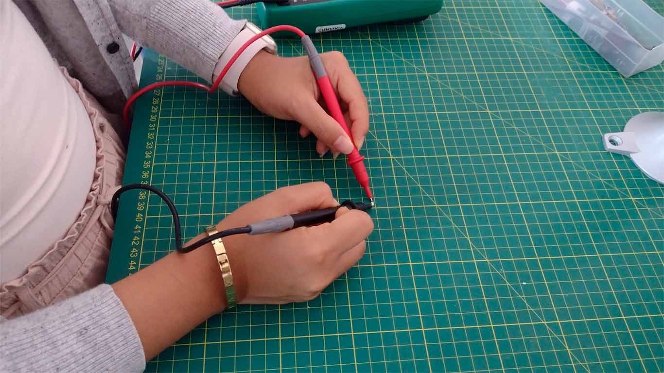
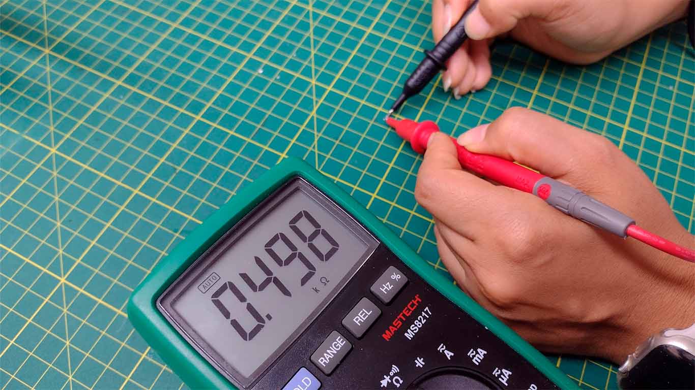
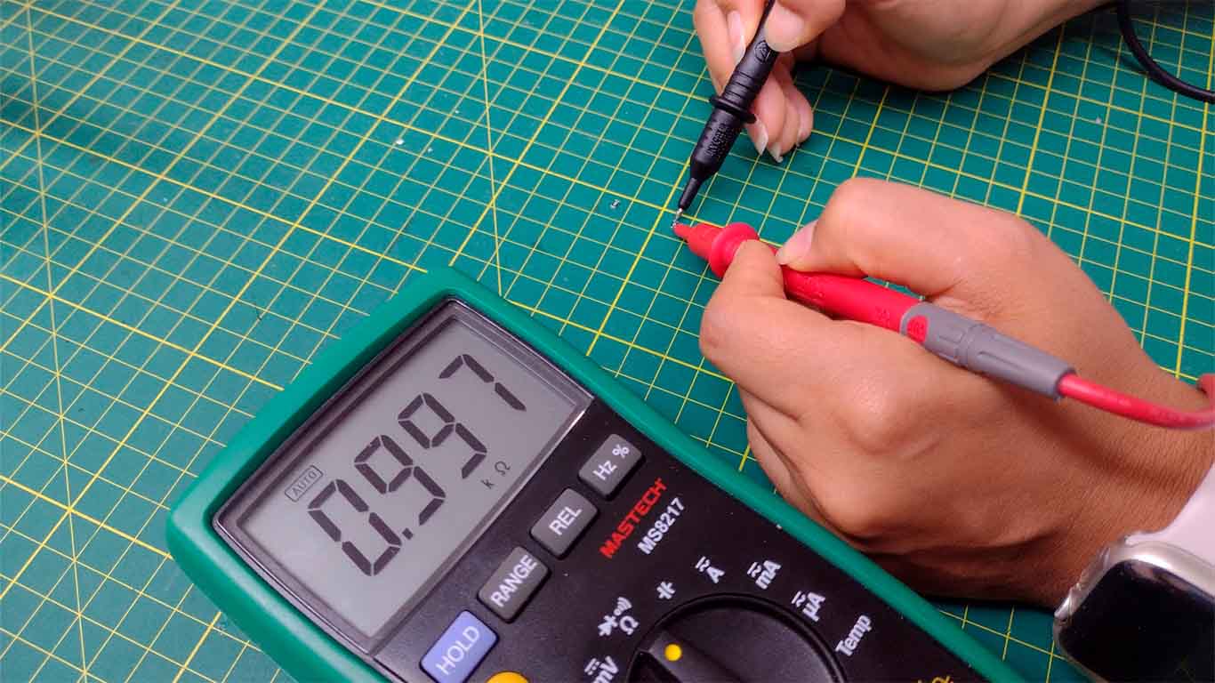
Now we will try with our resistors that we found in our FAB LAB. Here we will see the resistance that each one presents and the value they have according to the multimeter. To know how much resistance our components have, we have to go to the multimeter and choose the "Ω" symbol that means resistance, with this we can calculate it. Here our group tests.
For the test with the SMD resistors, we will use the 499 and 1K resistors, which will be tested by the multimeter to corroborate their value and we can see the resistance it presents.
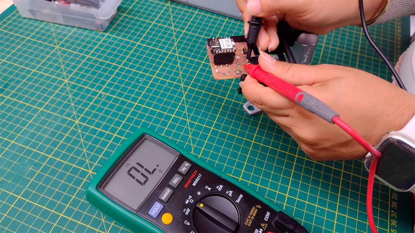
Now we will perform the CONTINUITY test in the QUENTORRES developed in week 4 of the FAB ACADEMY. Here we can see that the TRACES must have continuity and must be checked with the use of the multimeter. When the multimeter chooses the CONTINUITY symbol, it will emit a sound confirming that there is continuity, but if it does not emit it, it means that there is no continuity and the components are not connected.
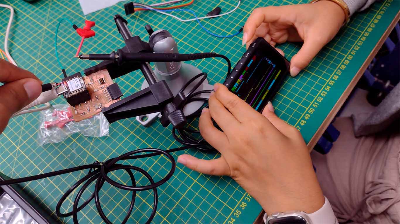
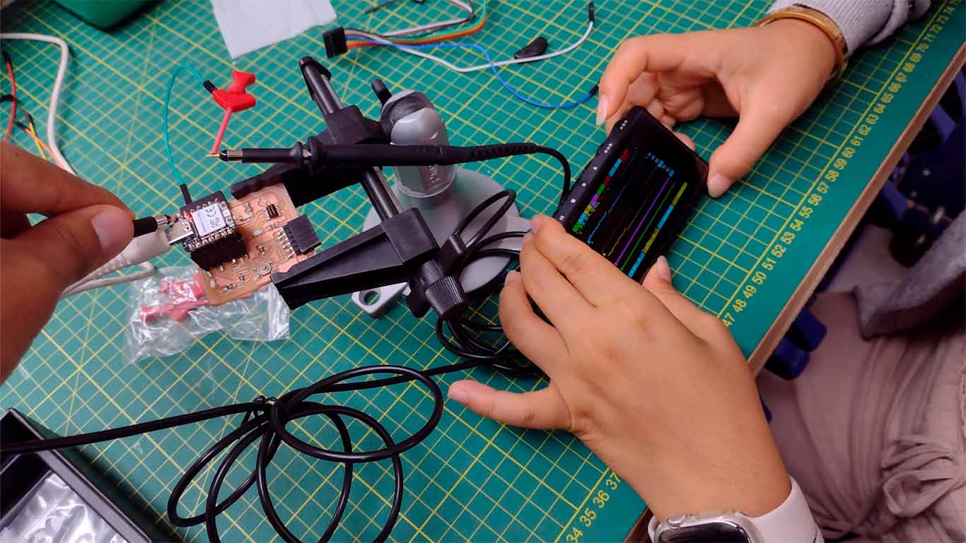
TESTING WITH LOGIC ANALYZER
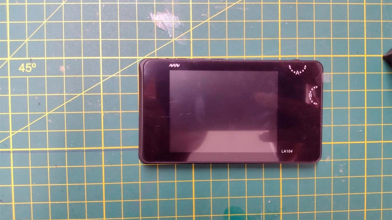
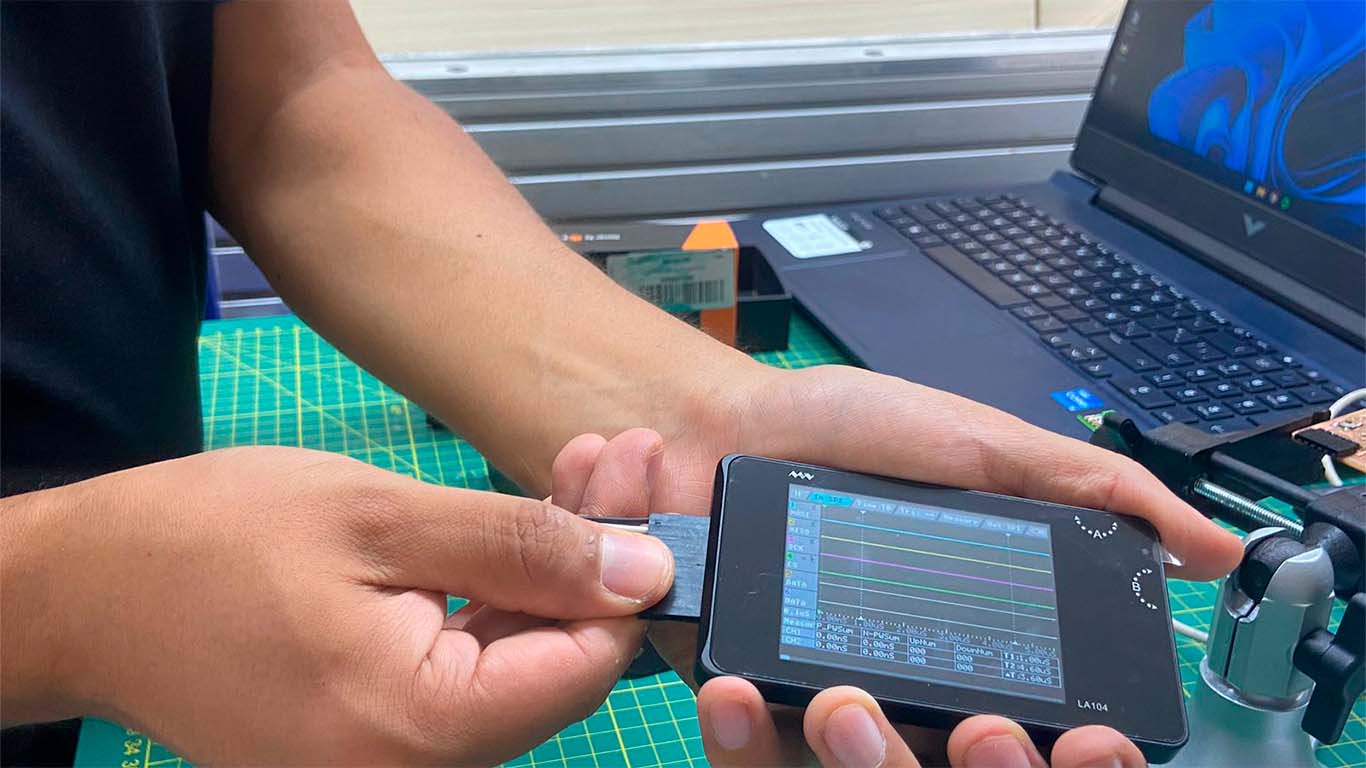
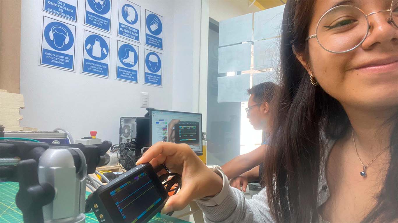
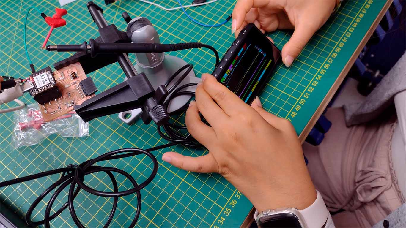
The logic analyzer that we have at the FAB LAB UCSUR is the LA104. Before starting to use it, they recommended that we calibrate it and configure it to start using it in the QUENTORRES. Likewise, we learned its management, configuration and how to interpret its data in order to analyze the behavior of digital signals. Here are some photos before using it.
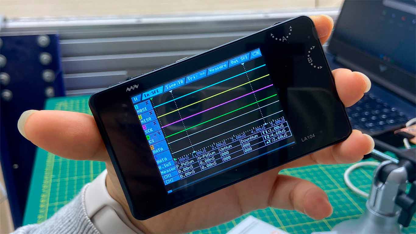
After configuring the equipment, we used it in the QUENTORRES where we could visualize the behavior of the board. We observed the digital signals that the board could read on some components of the board and understood that the board did not present any problem in device communication.
For the test with the logic analyzer, connect the GND and Channel 1 to the Quentorres board to know the graphic representation that we have when we perform the test.
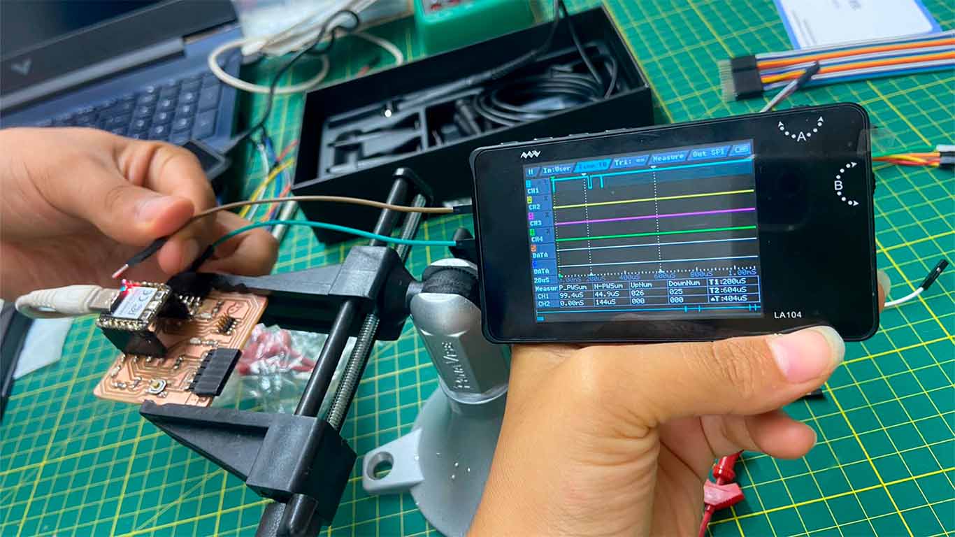
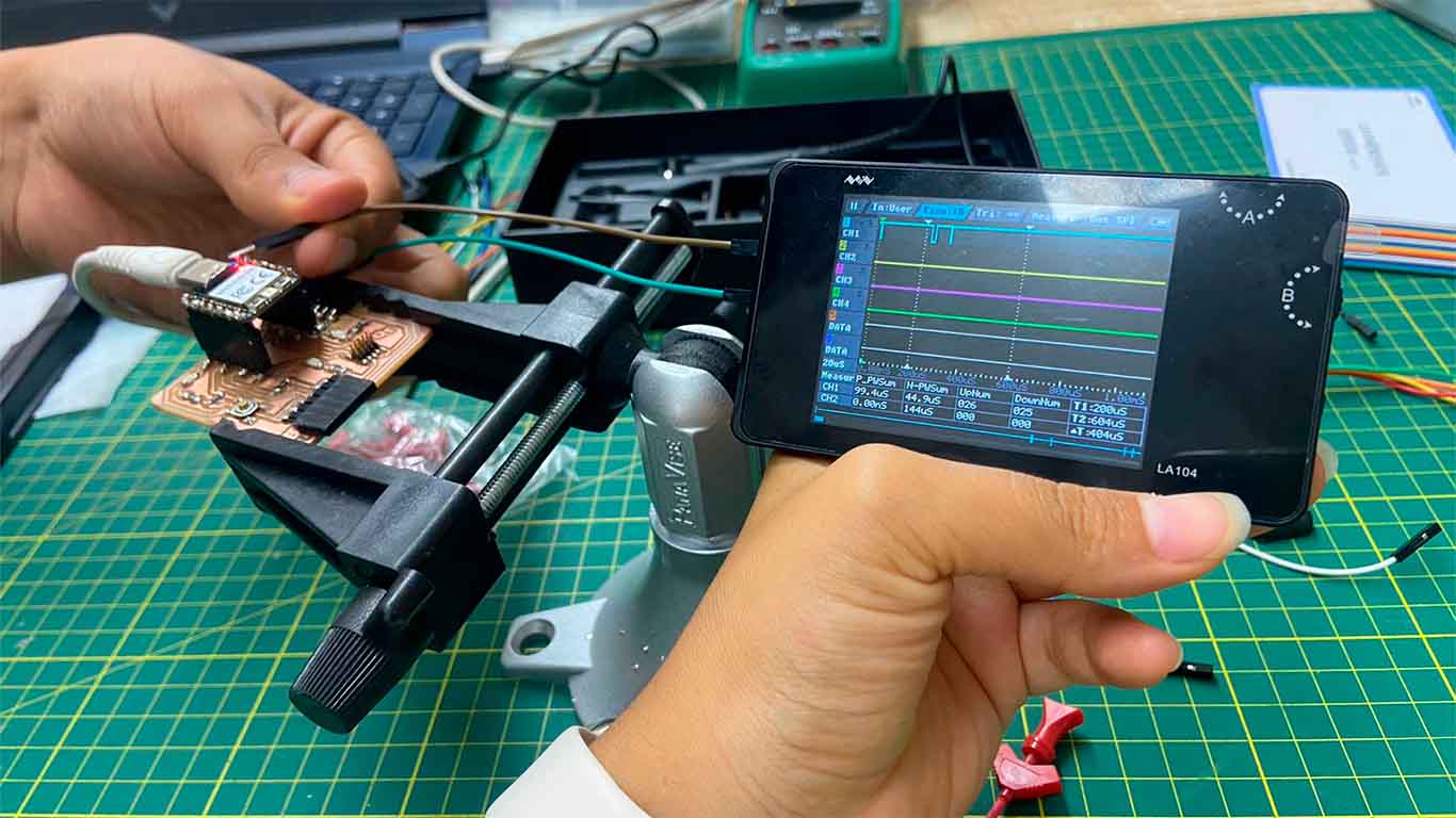
As a result we obtain square signals on channel 1, where we can conclude that the QUENTORRES sends binary digital signals when we make contact with one of its pins and where we can see the communication protocol it is doing.
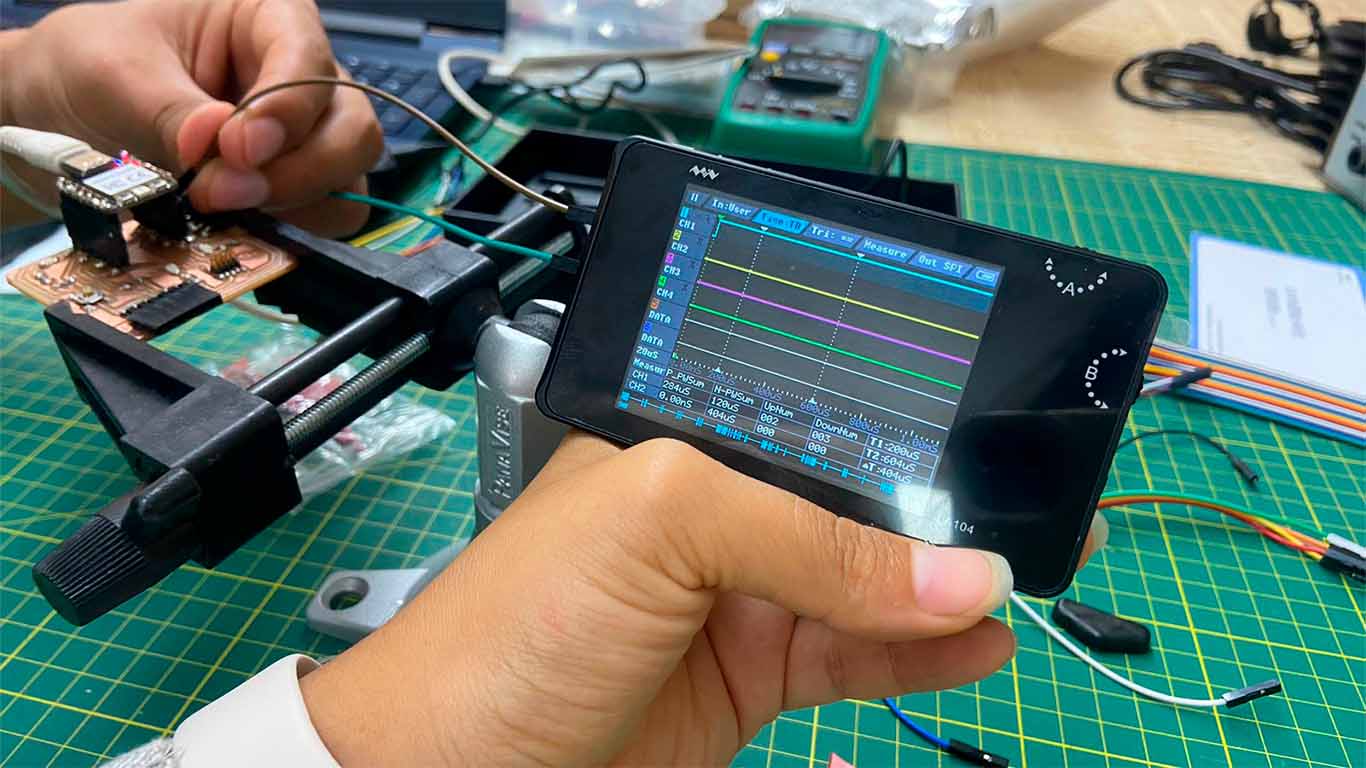
TESTING WITH MINI OSCILLOSCOPE
Now we will use the MINI OSCILLOSCOPE that we have in the FAB LAB. We will also try it on the QUENTORRES plate. My friend Maryori gave me this selfie that I didn't realize she took because we were watching videos, some previous documentation to know how it is used and how we can analyze the plate with this tool.
After studying the tool more, we applied it in the QUENTORRES where we were able to know, visualize and analyze the electrical signals of the board when we make contact with it. The truth is that it is very interesting to know how the different behaviors that the components have are shown and see electrical signals. Here are some photographs we took when performing the test.
As a result of the tests applied to the QUENTORRES we obtain sine waves which means that the board provides AC alternating current signals generated by the components found on the board.
TESTING WITH DC VOLTAGE SUPPLY
For the test with the voltage supply we perform it with a servomotor to know its operation. First we understood the parts of the machine and then we connected it with the servomotor on their respective positive and negative pins.
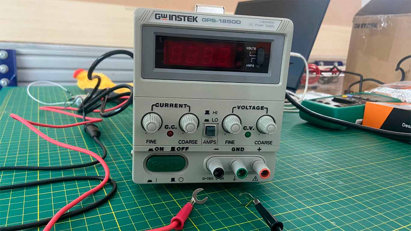
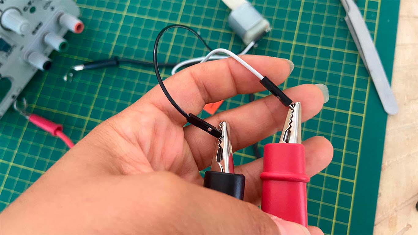
Connect the servomotor cables with the voltage supply machine using hooks.
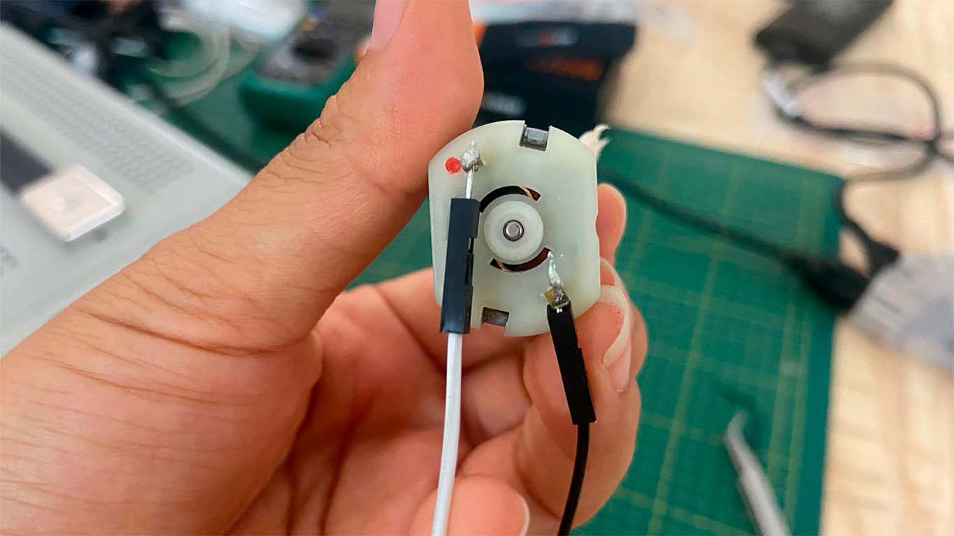
In order to better see how it works, we glue a tape to the servomotor to see its movement and the change it makes when we change the current and voltage it receives.
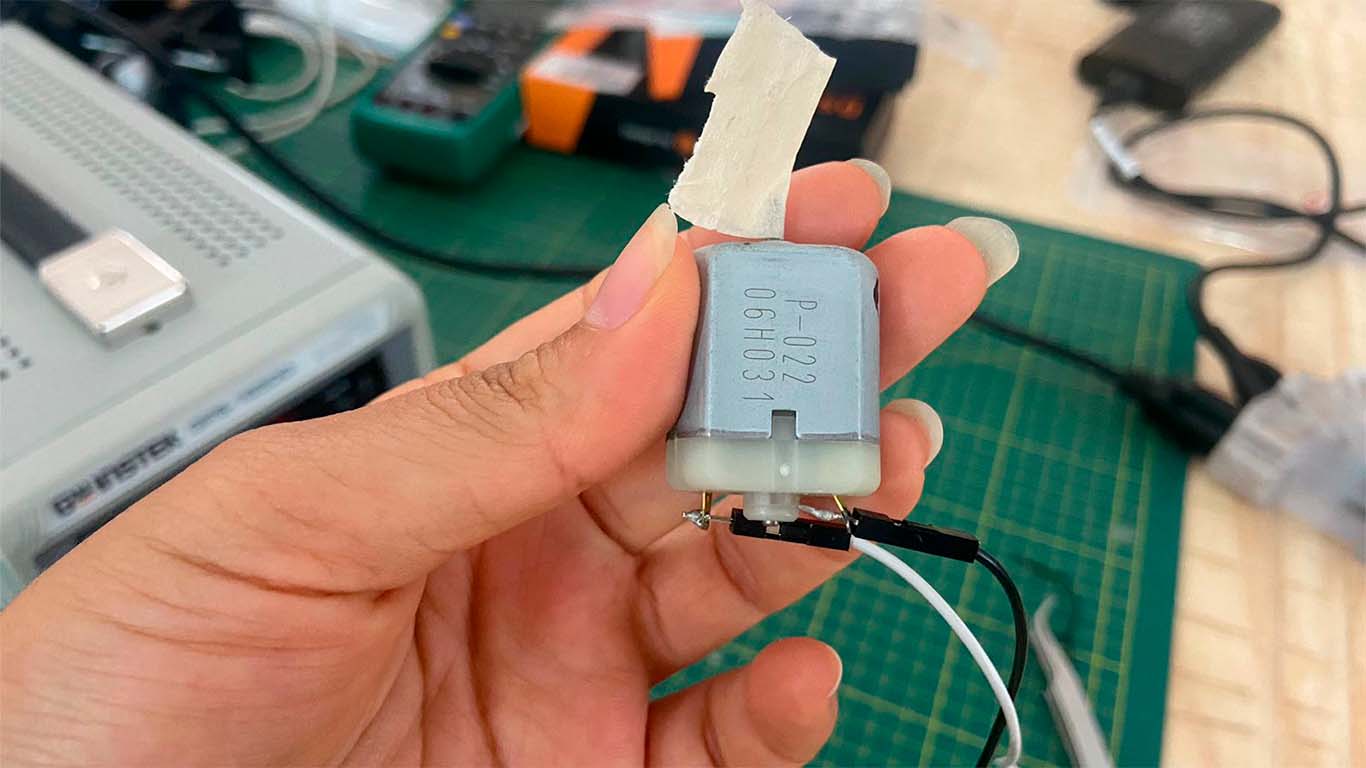
Here I show you a video of the result of how we can change the current and voltage so that the servomotor increases or decreases in speed. Here we can understand how the current and voltage work in the components.
SUPPORT AND FEEDBACK
FAB ACADEMY SUPPORT
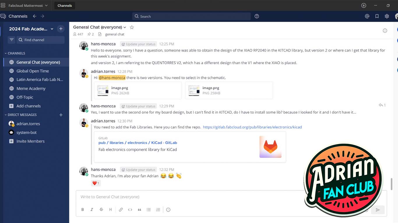
First of all, remind you that at FAB ACADEMY you are never alone and there are colleagues who support us on our path. For example, teacher Adrián is one of the people who supports us and gives us that support when we feel stuck. Here is a photograph of how he supported me to achieve this assignment and from now on I consider myself a fan of Adrian. Also thank you for your support in the GLOBAL OPEN TIME on Saturdays.
FEEDBACK
Before developing the assignment, teacher Ulises gave us a small electronic design class, where he first explained to us the operation of the QUENTORRES, its design and the explanation of the components. Then, he taught us how to use KICAD 8 and how we can start designing our board for the assignment.
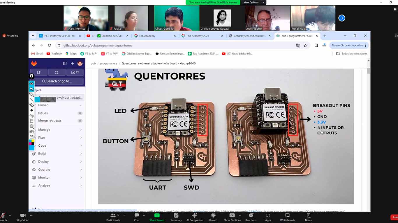
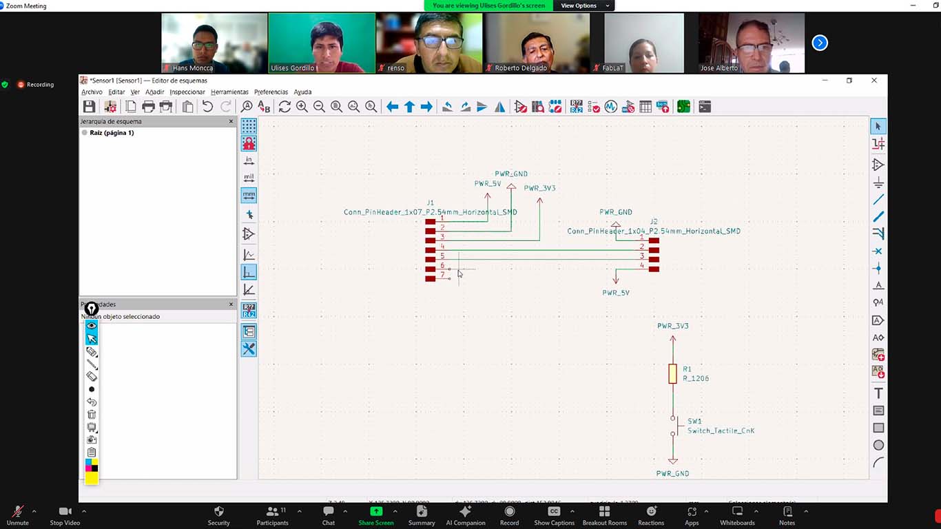
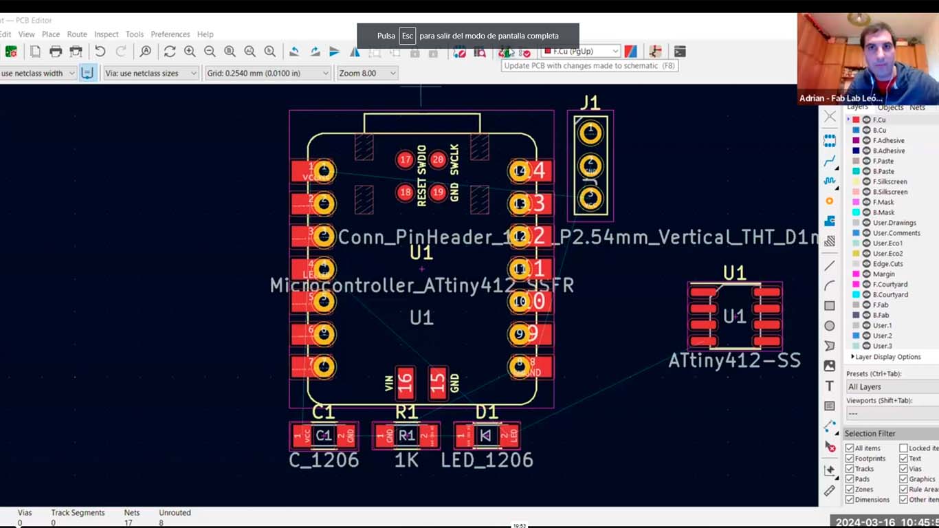
Finally, at the GLOBAL OPEN TIME on Saturday 03/16 they showed us how to use the KICAD program and how we could start designing our board for the assignment. The truth is that all the teachers support a lot to be able to achieve each assignment and I recommend students and future students of the FAB ACADEMY to join the GLOBAL OPEN TIME. The truth is that it helps a lot to remove doubts and with great experts. Thank you Adrian and Rico for every teaching.
INDIVIDUAL ASSIGNMENT
IMPORT OF FAB LIBRARY TO KICAD 8.0
FAB LAB LIBRARY FOR KICAD 8.0
Before showing you my board design I want to start by showing you how you can import into KITCAD 8.0 all the FAB ACADEMY information that is necessary for this assignment and develop your boards in the future. Here I show you the steps and maybe it can help someone else.
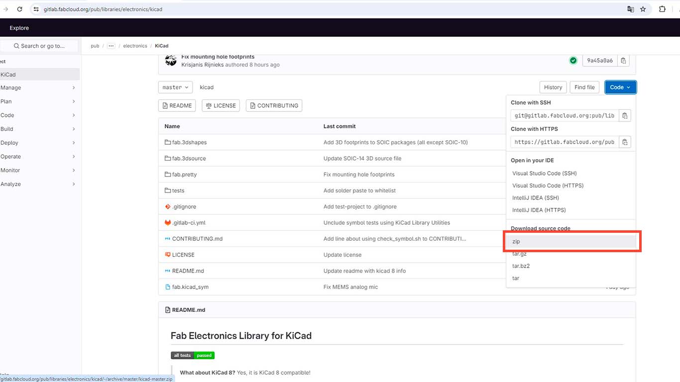
To have the XIAO RP2040 and the other components that we will use for the design of our board, we need to download and import the entire FAB LAB library into KICAD. Therefore, first we will go to the download link that I will leave here. LIBRARY LINK
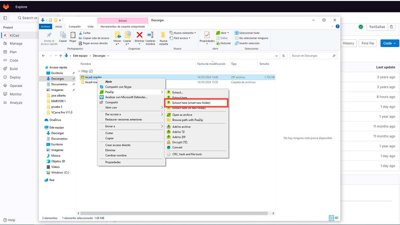
Then, we download it in ZIP format to obtain the liberia files as shown in the photo.
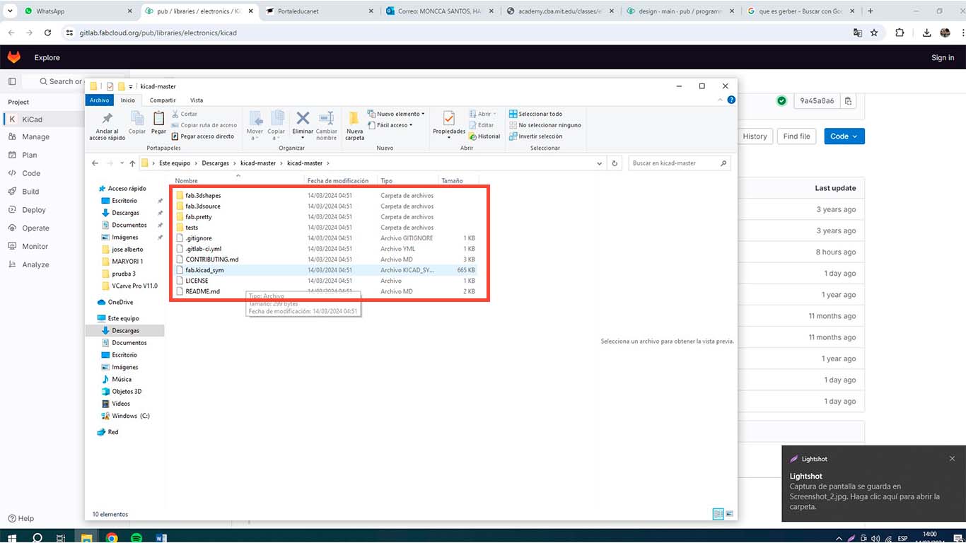
Now unzip the ZIP file into a folder and when we click on it we have to check that all the files that we found in the previous link are there.
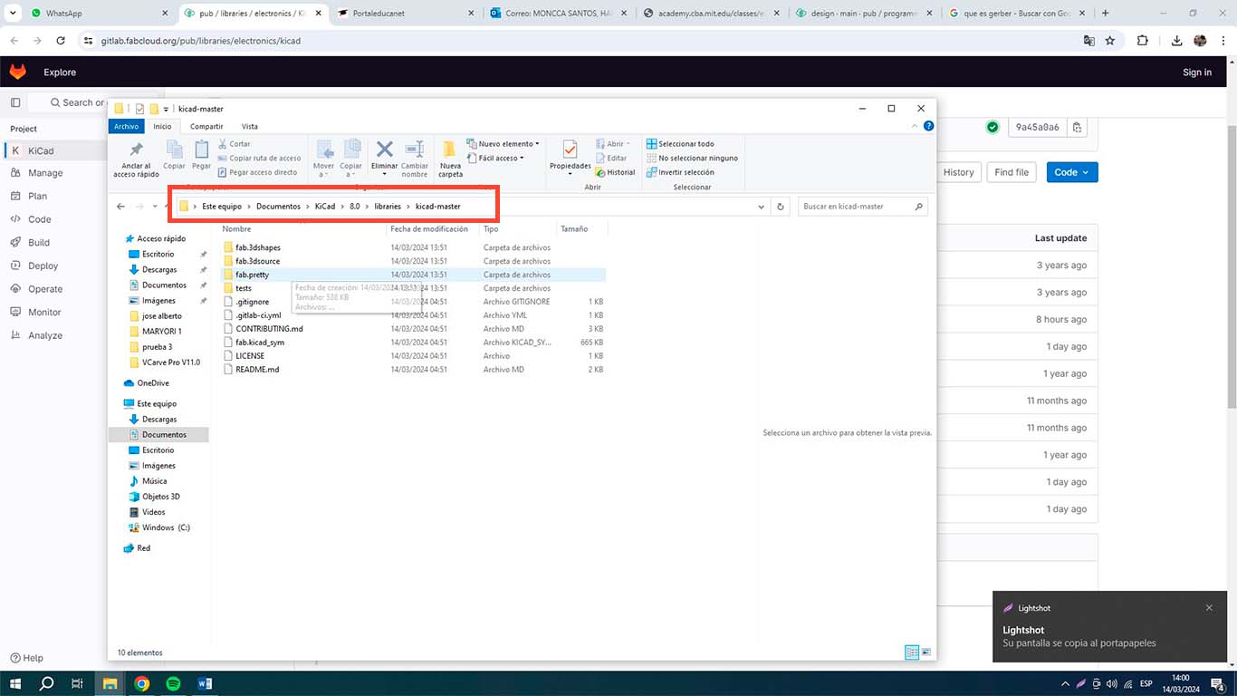
Now we have to copy the entire compressed folder to the following address: DOCUMENTOS/KICAD/8.8/LIBRARIES, if we do not have the LIBRARIES folder, we can create it and inside it paste the entire folder that we compressed previously. This step is important to be able to import all the component information into KICAD.
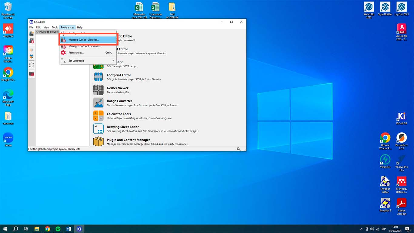
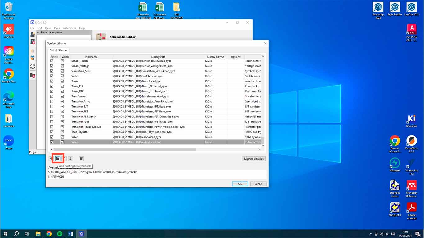
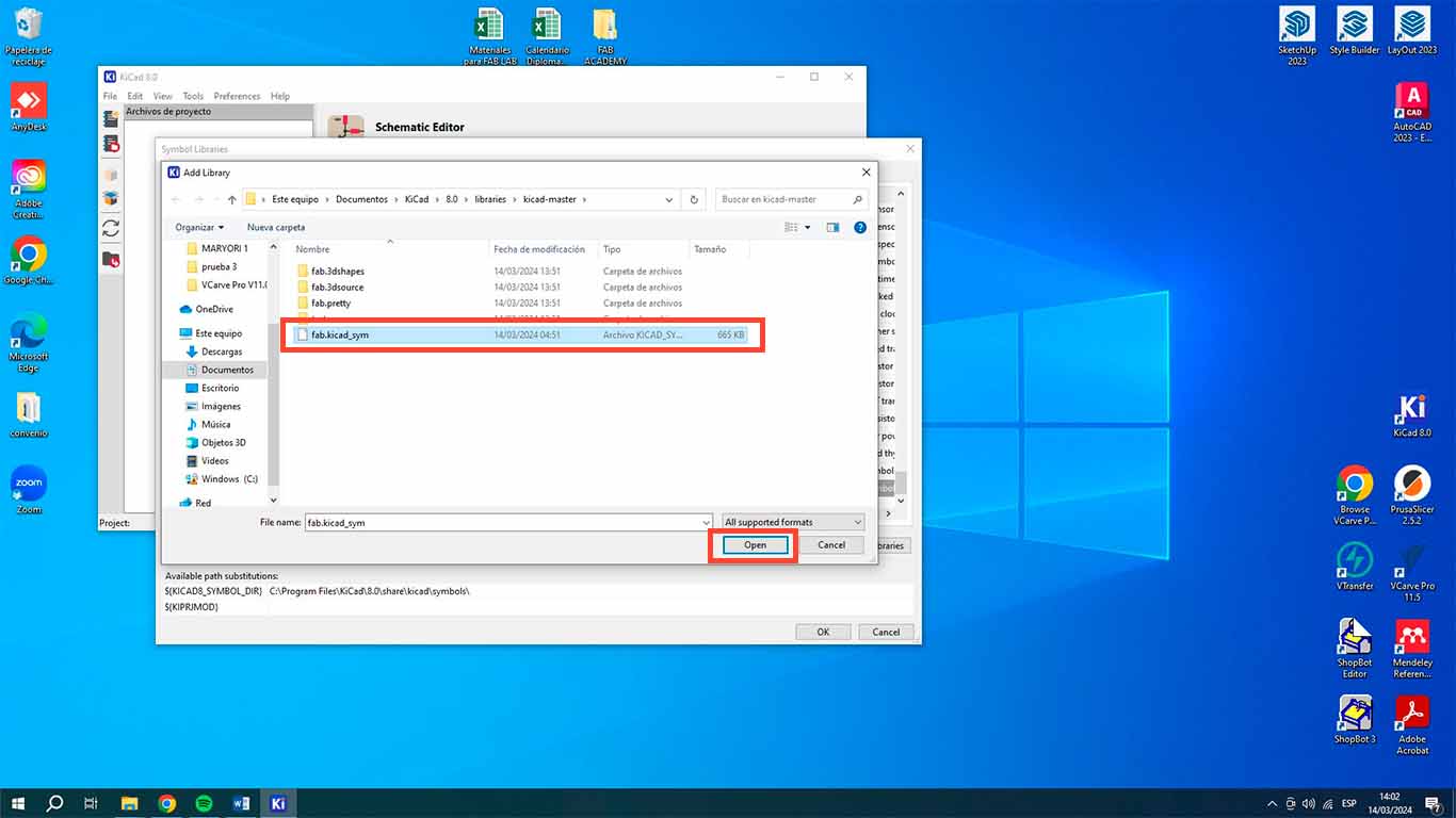
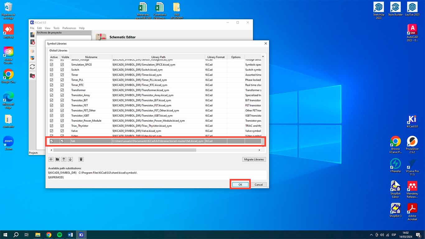
Now we open KICAD and go to the PREFERENCES tab, where we will choose the MANAGE SYMBOL LIBRARIES option, here we click on the FOLDER symbol, we look for the file called FAB.KICAD.SYM and we click OPEN. Here we will see that it has been added to the entire list of liberias and finally we click on OK
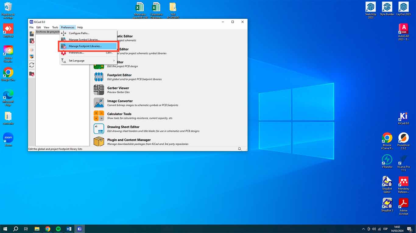
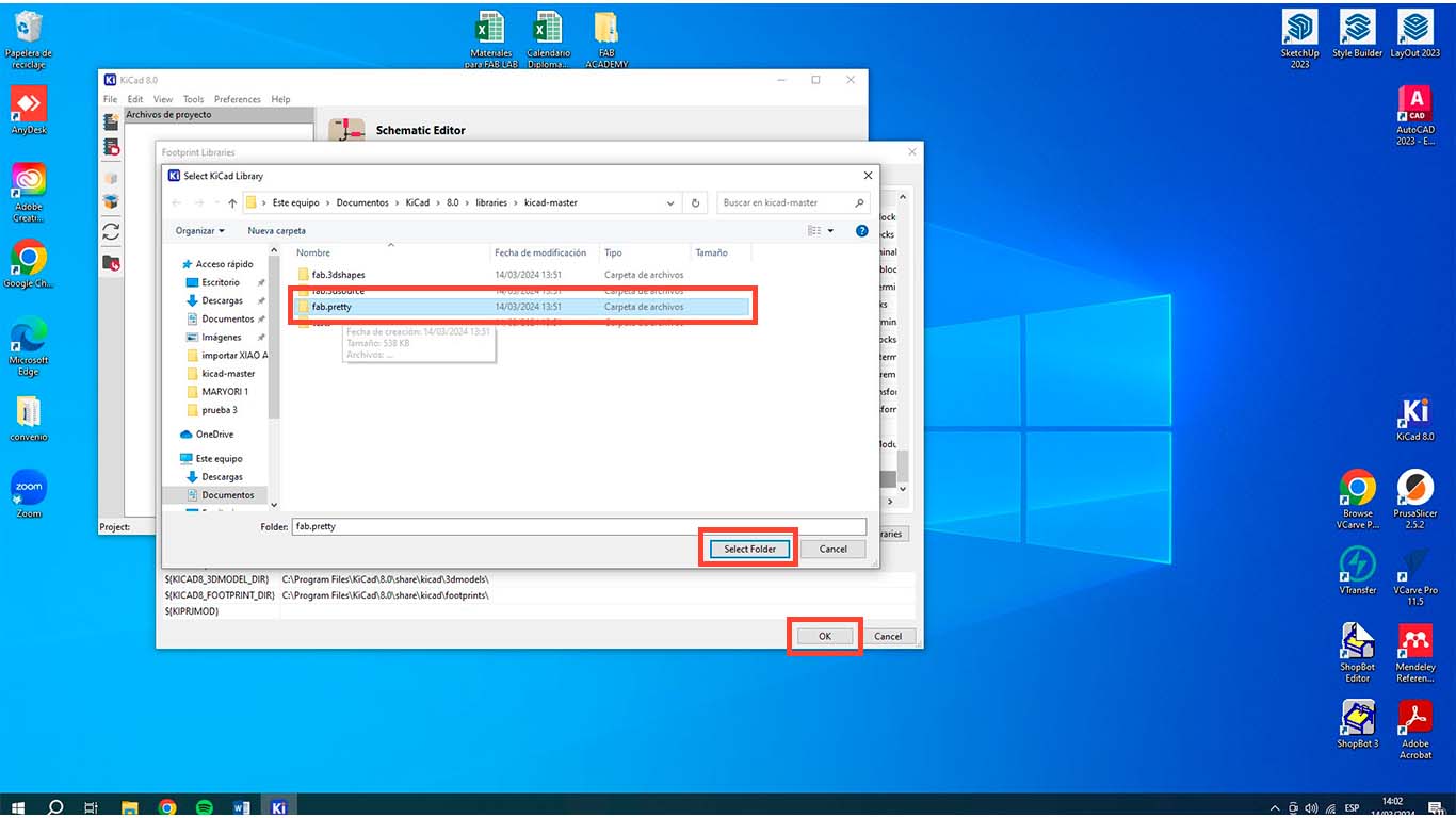
Then to add the FOOTPRINTS, we look in the PREFERENCES tab for the MANAGE FOOTPINT LIBRARIES option, when we click on it, we go to the FOLDER symbol to add the entire library and we choose the folder called FAB PRETTY. Finally we just click on SELECT FOLDER and OK.

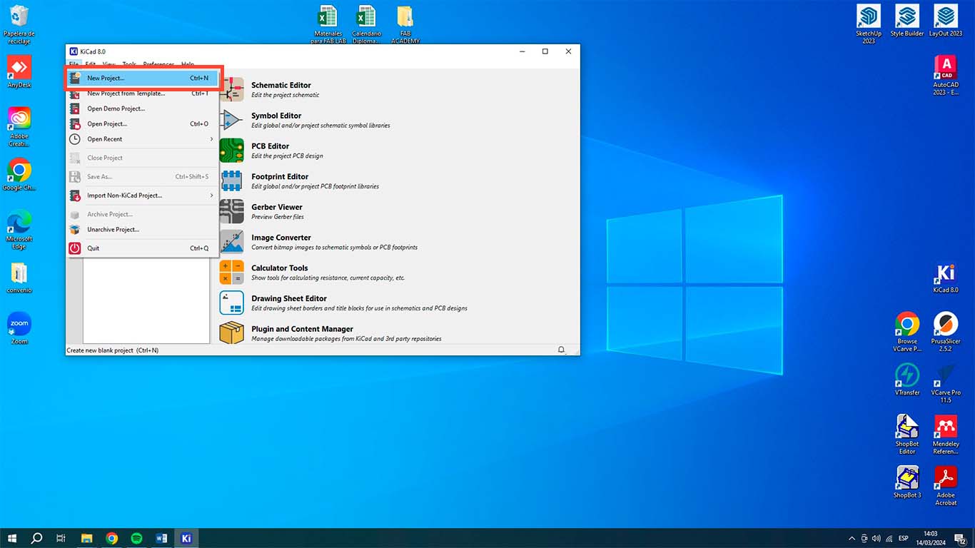
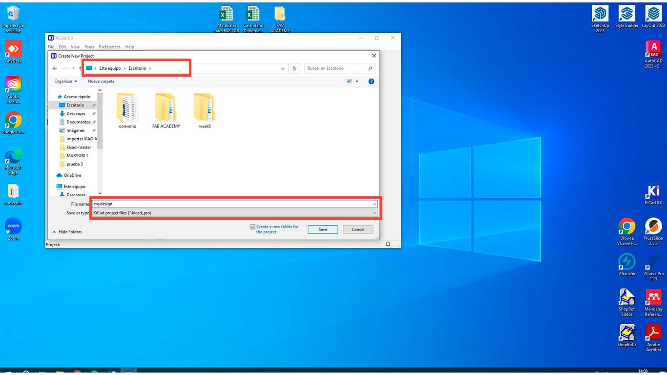
Now to check if the libraries have been installed correctly, we go to the FILE tab and click on NEW PROJECT. From there we will choose a place where we want to save our new project, in this example I will do it on the desktop and click SAVE.
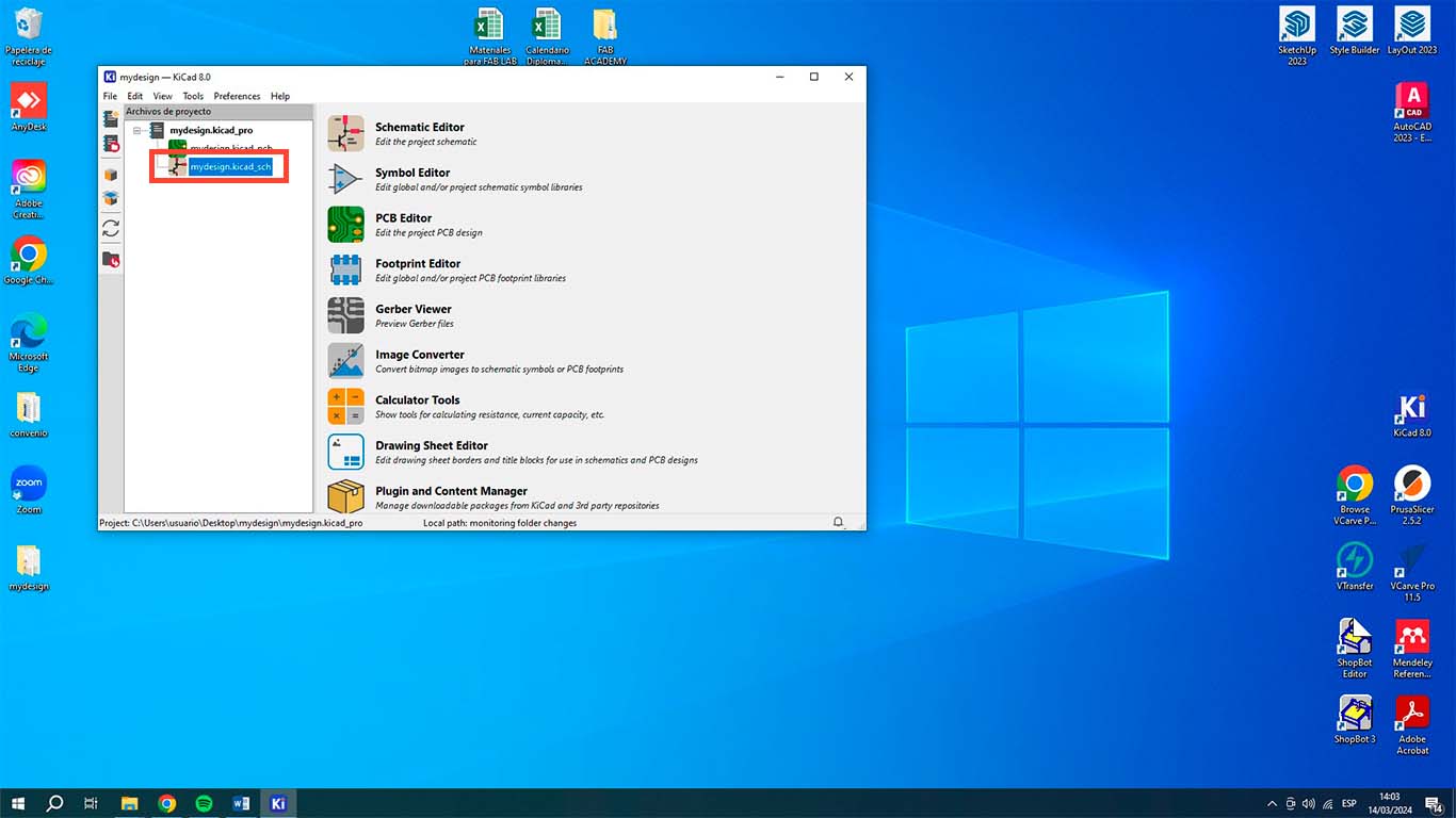
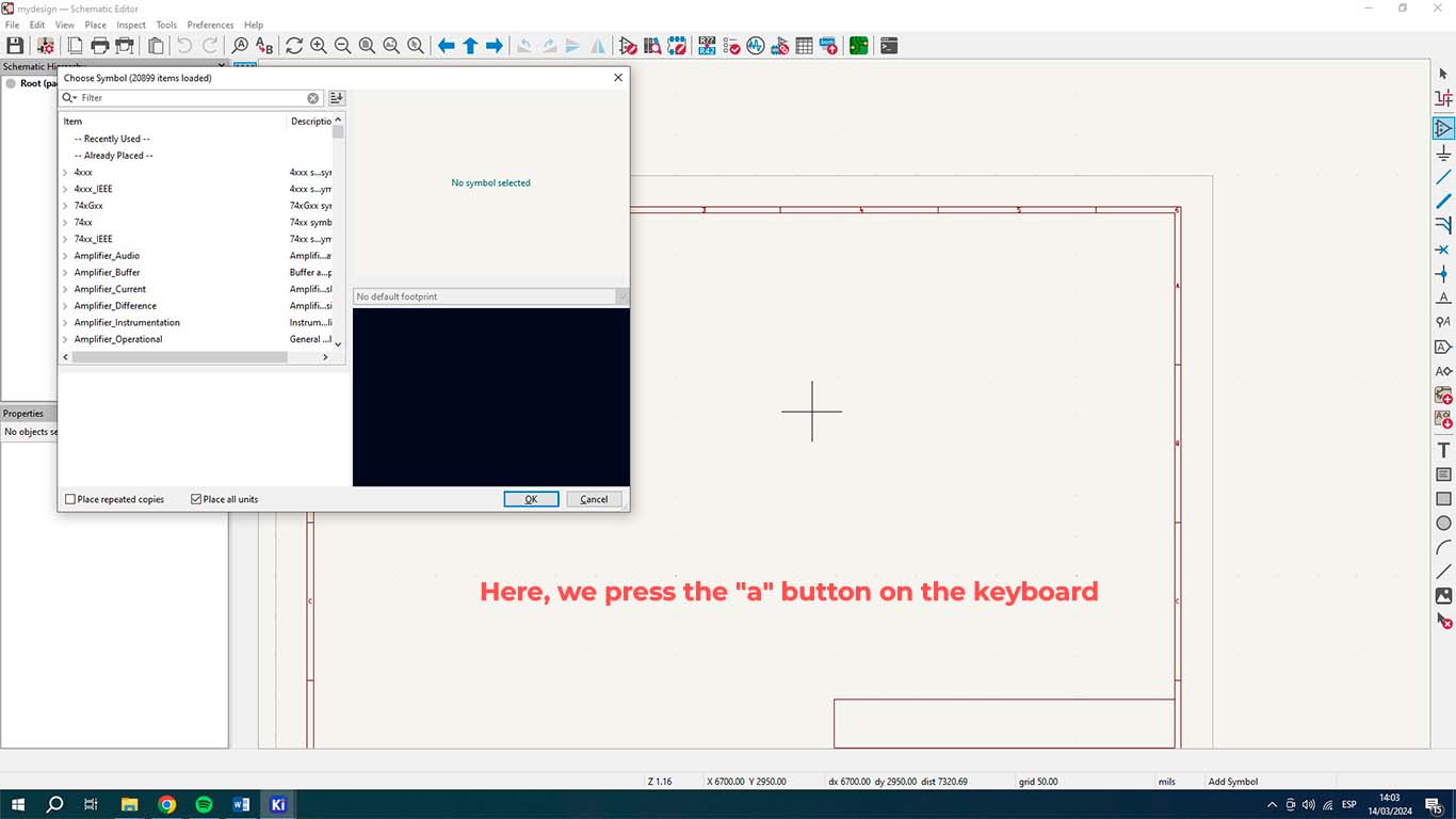
When we have the previous step ready, we will choose the file of our new project that has the NAME.SCH, which means that it is the schematic design of our project.
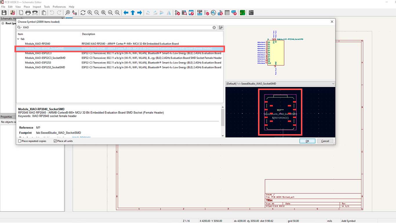
When we are in the file, we press the letter A on the keyboard and a tab will appear of all the information that KICAD has so far. There we can write XIAO and we have to get the RP2040 component.
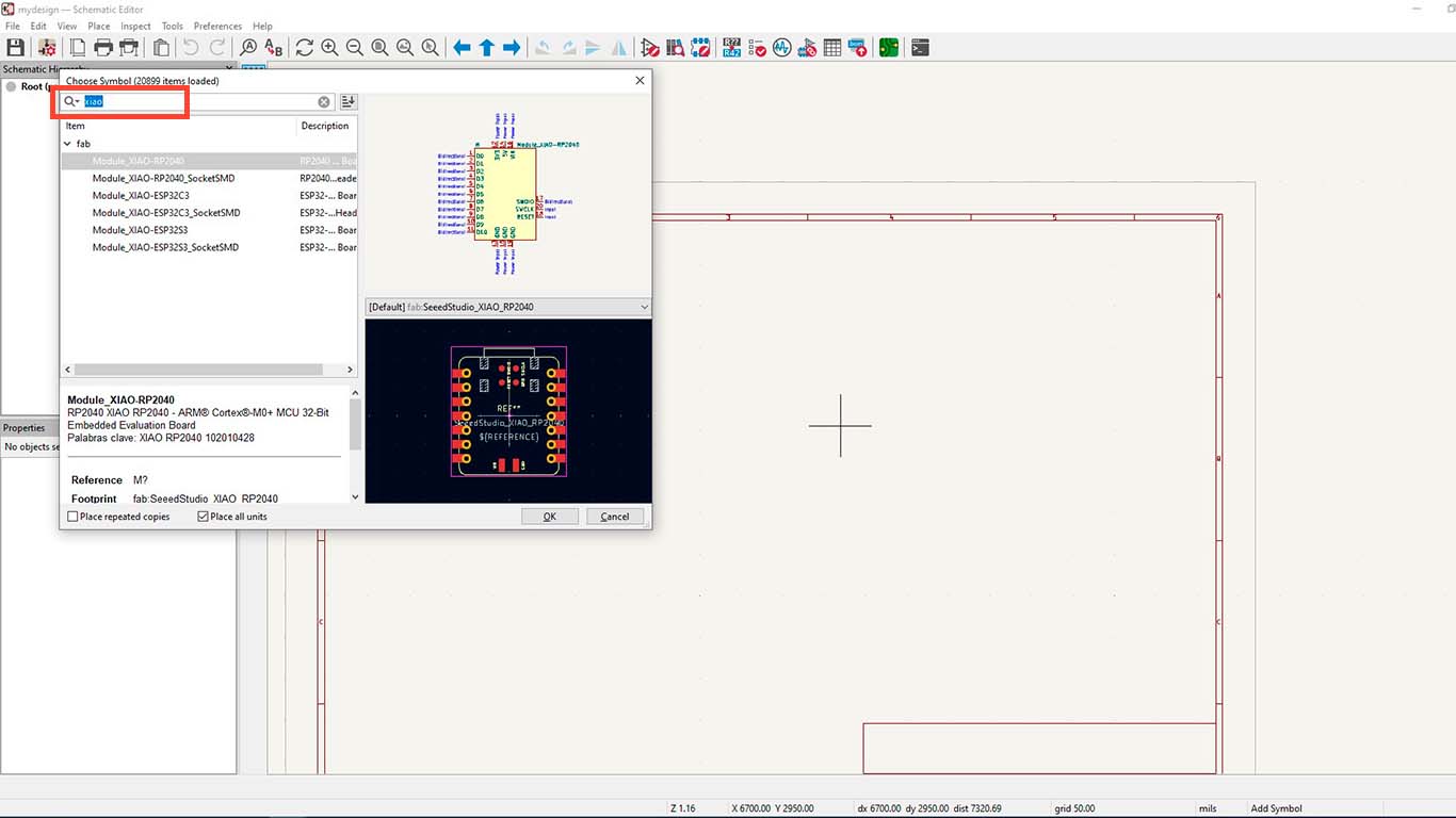
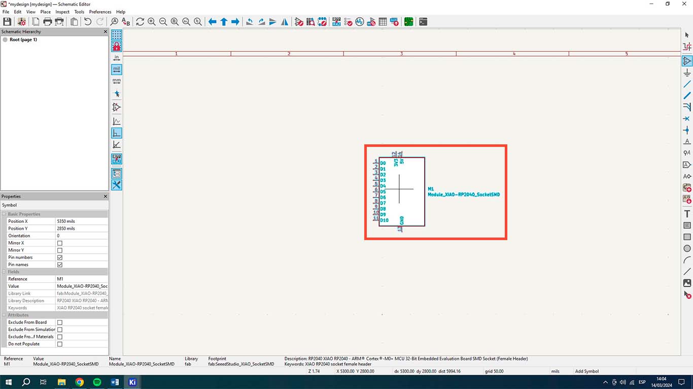
We can see that the Liberia was imported into KICAD and we can now start working with the SOCKETS of the XIAO RP2040 and other types to develop our boards.
Finally, to check that we can also see the XIAO RP2040 in the design area, we go to the top and look for the OPEN PCB IN BOARD EDITOR option
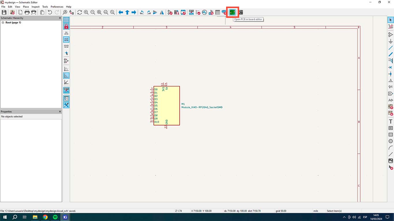
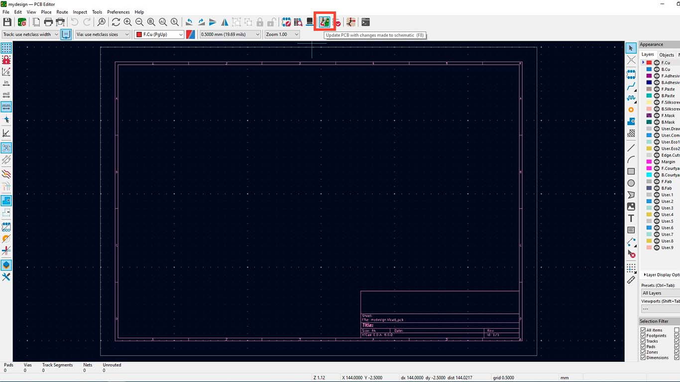
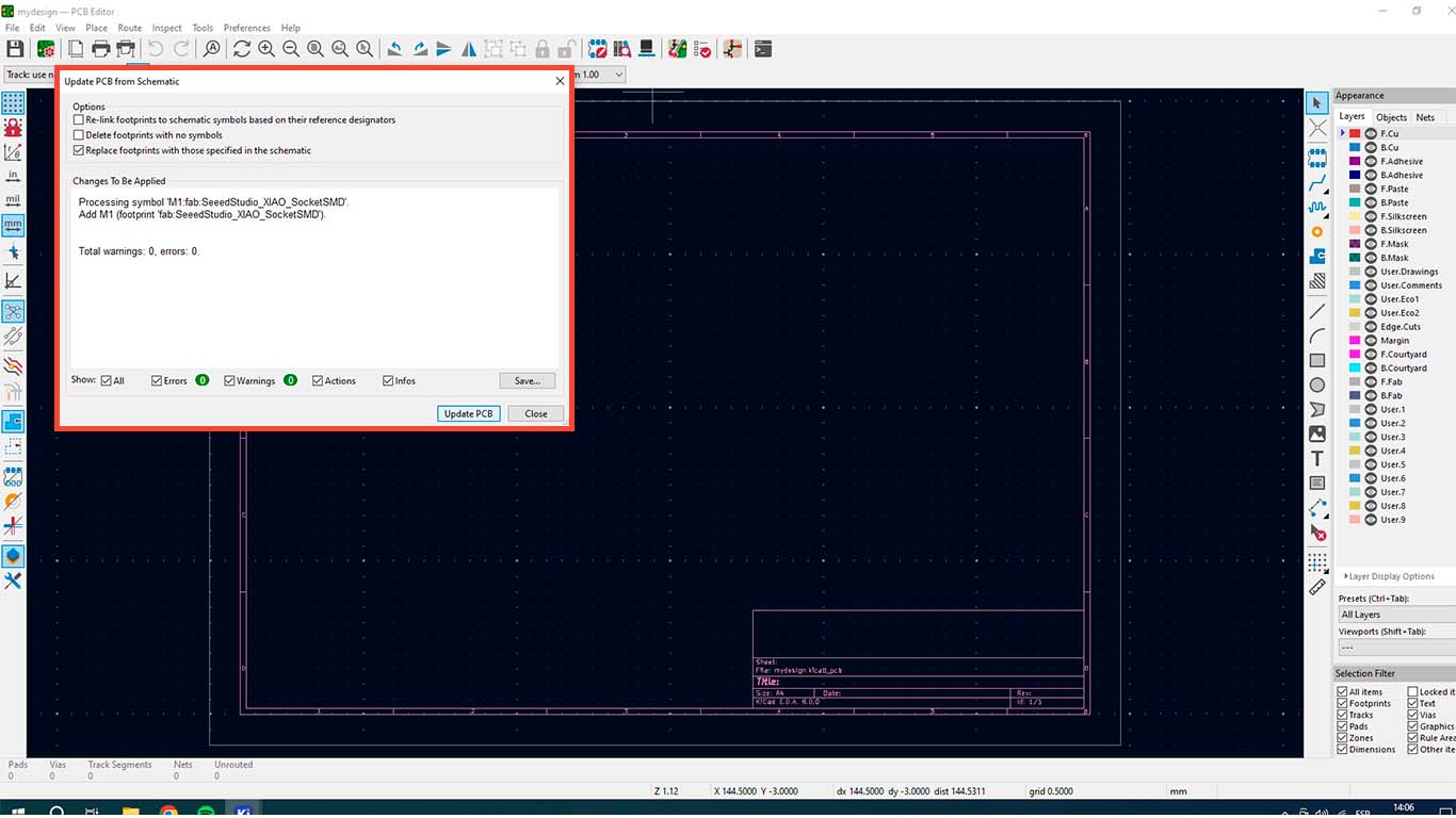
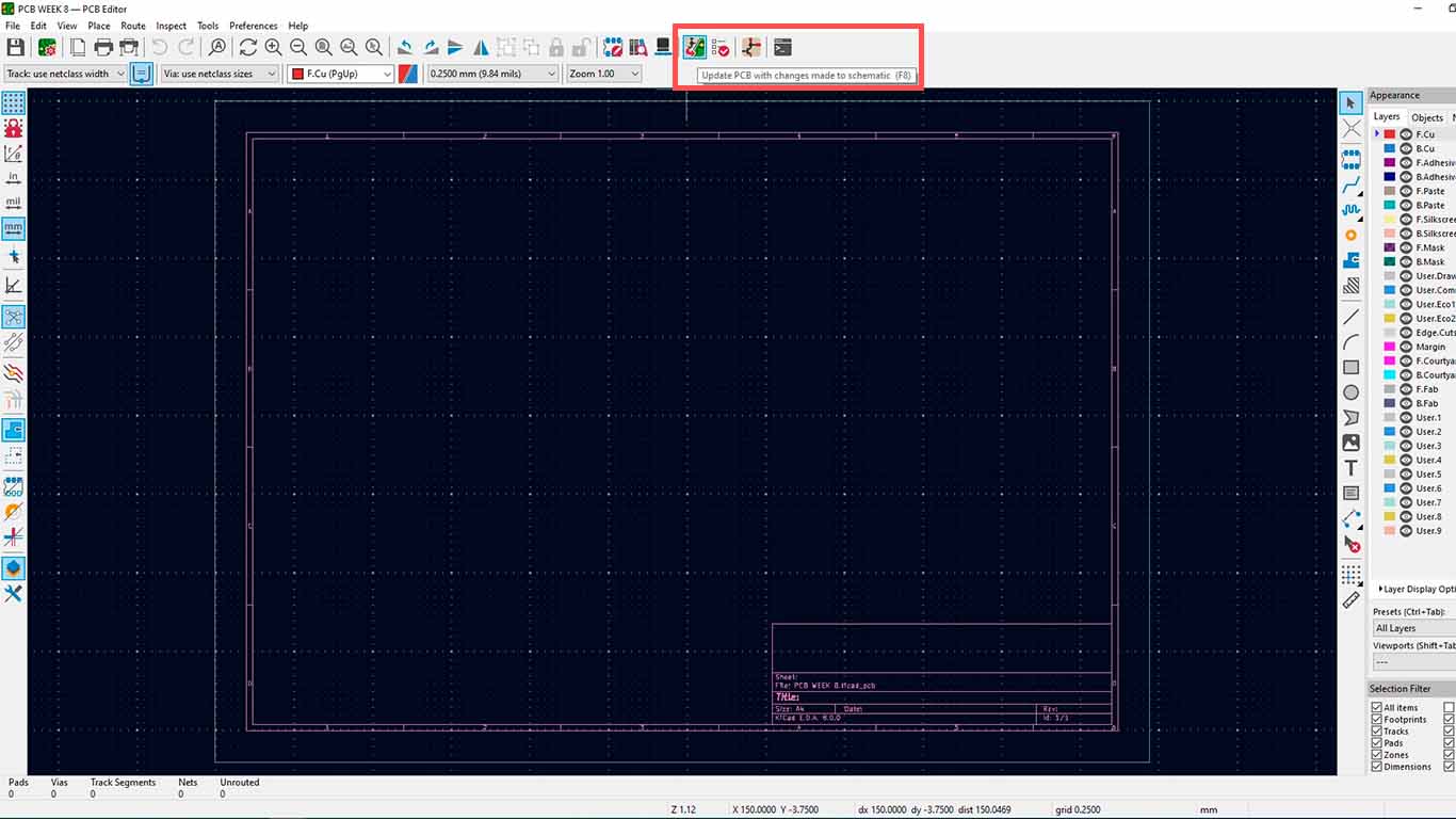
The PCB EDITOR will open and to import our work done in the schematic area, we click on the UPDATE PCB WITH CHANGES MADE TO SCHEMATIC option.
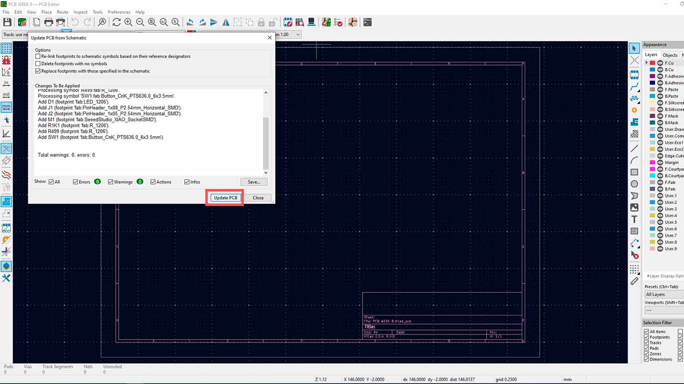
A window will appear where it will tell us if the components were imported correctly into the design area. And if everything is fine, we click on UPDATE PCB
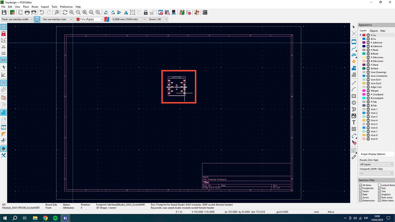
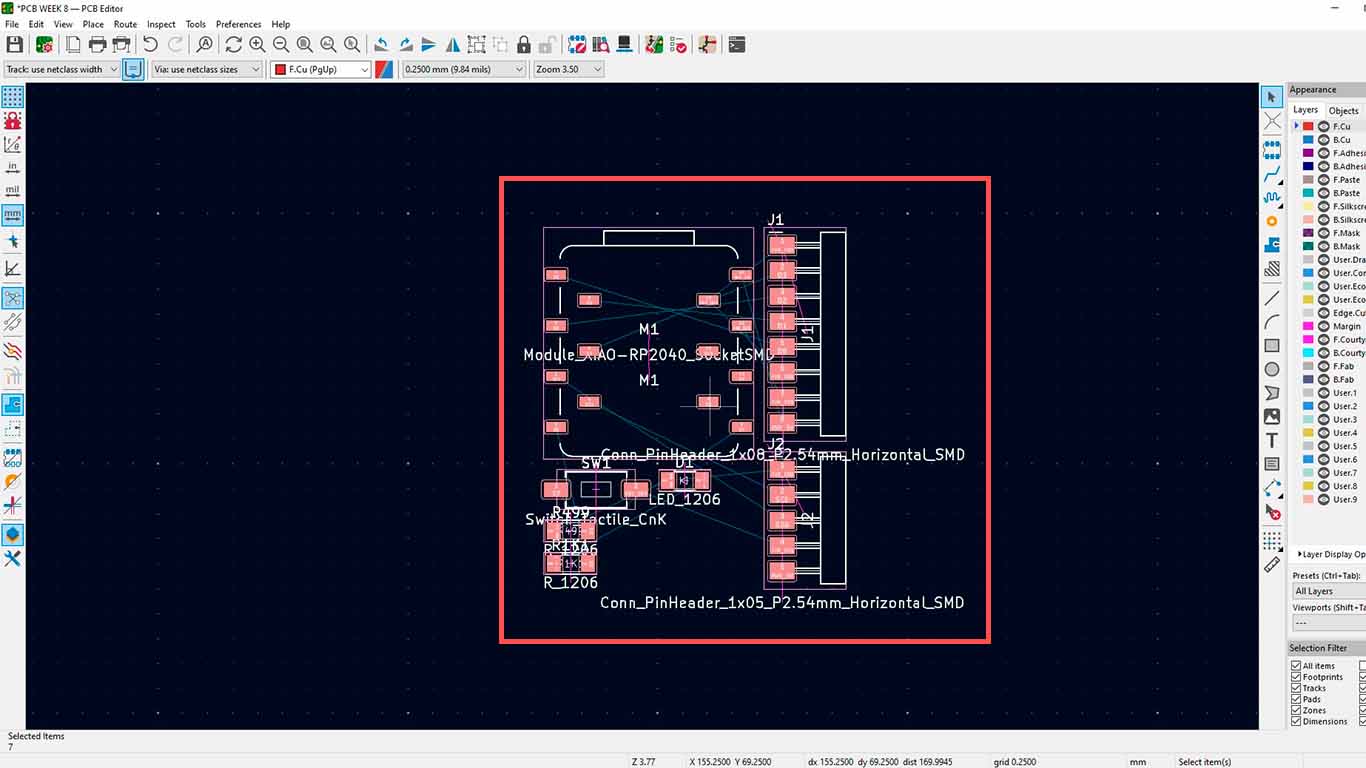
Here we can see that in the PCB EDITOR we obtain the FOOTPRINT of the XIA RP2040 and we are ready to start our individual project
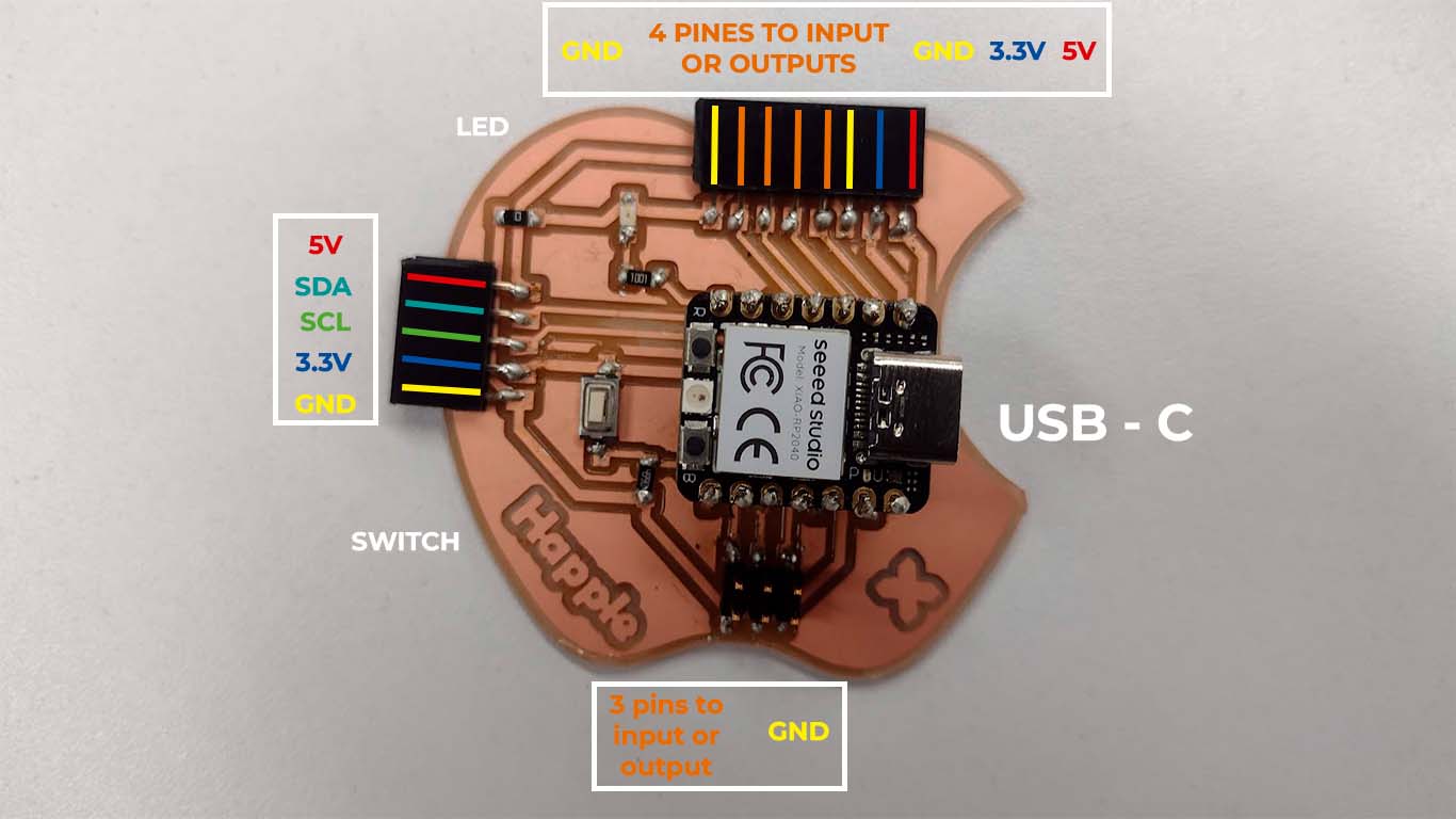
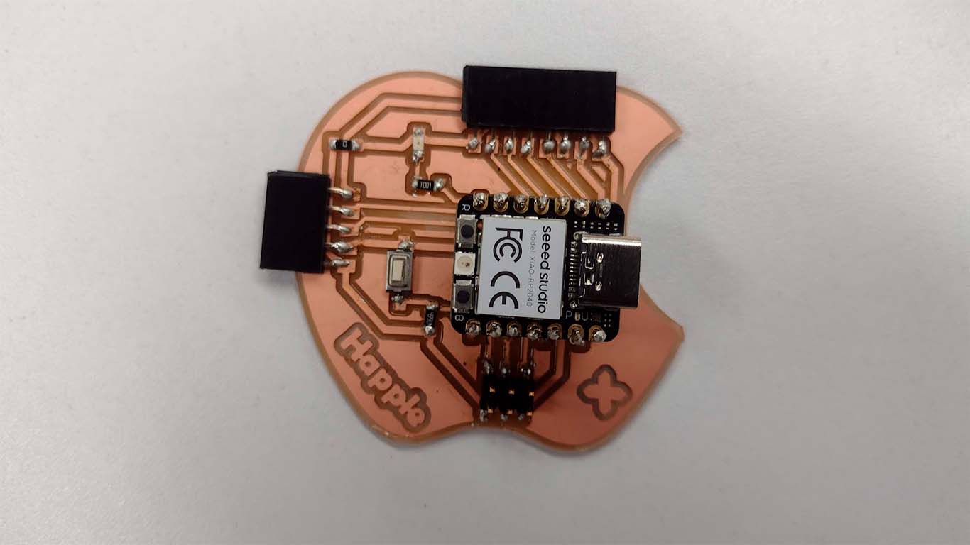
DESIGN 1: HAPPLE X
HAPPLE X: MY DEVELOPMENT BOARD
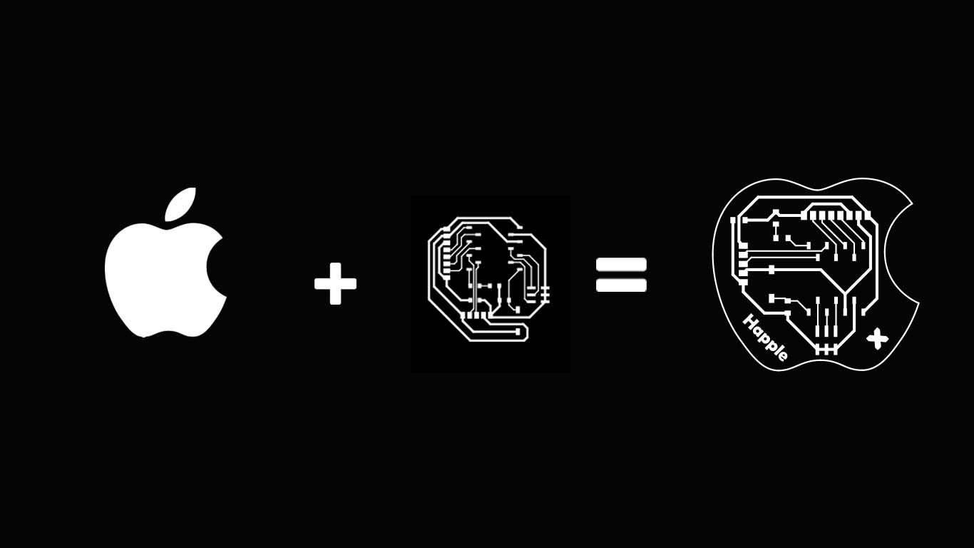
For the next assignment I wanted to have my own development board so I could program different inputs and outputs for the following weeks. For this reason, Happle X was born, a board that wanted to have different inputs and especially to program with the SDA and SCL pins. The shape of my board is especially due to the technological brand that became very related to me when talking about electronic design.
Here I have the distribution of the pins, GND, 5V and 3V3 on the HAPPLE X board.
REFERENCES
I had never designed a board, so I was greatly inspired by the boards developed by Adrian. Especially the QUENTORRES and the FAB-XIAO. I took them as a reference since they use the XIAO RP2040 microcontroller and it is the only microcontroller I have to program. I find them very interesting since you can program almost all the components that we can learn about in the FAB ACADEMY.
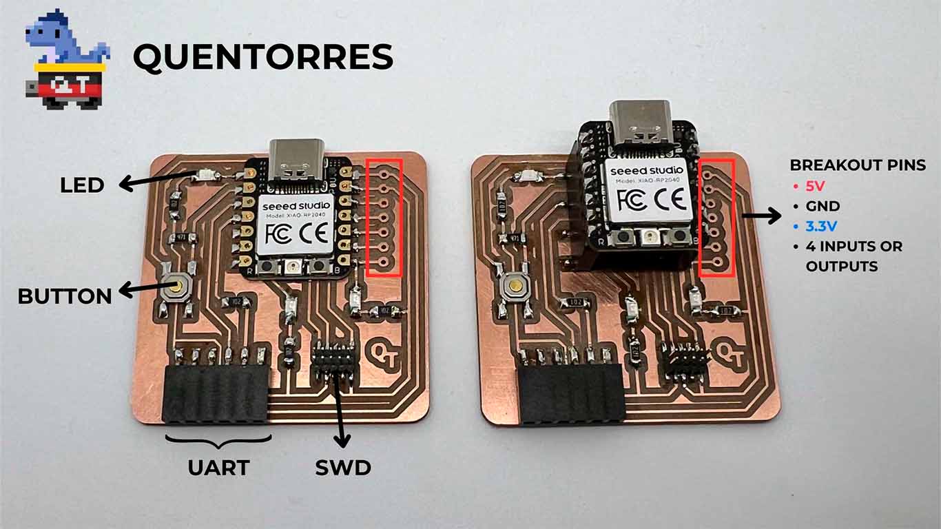
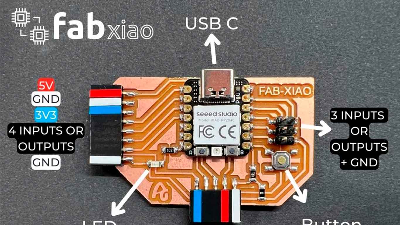
Here I leave the links to each of them. FAB-XIAO y QUENTORRES
HOW I DID IT IN KICAD
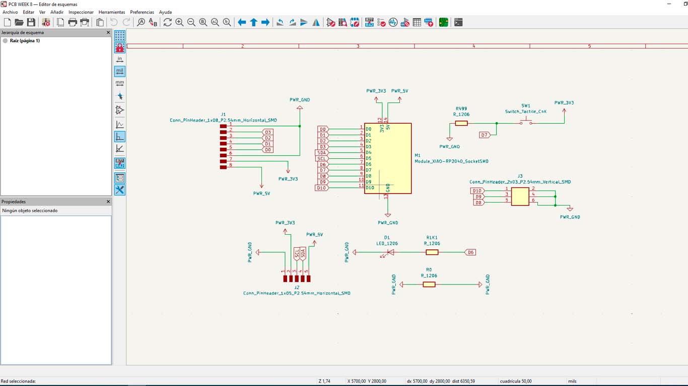
For my electronic design I used the KICAD program. Let's start looking for the XIAO RP2040 in the program library and this time I want the XIAO RP2040 to have the TYPE 2 version of the QUENTORRES, that is to say that it is not soldered on the front of the board, but it has vertical connectors to place the microcontroller, that's why I chose version 2.
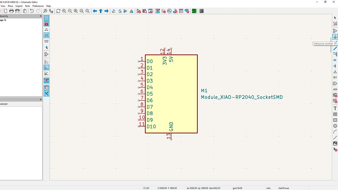
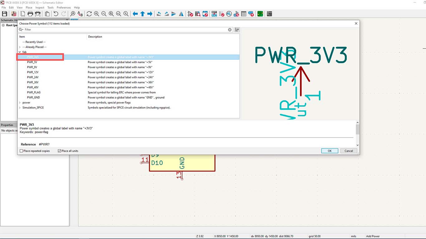
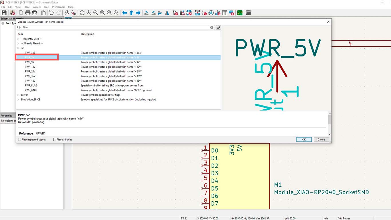
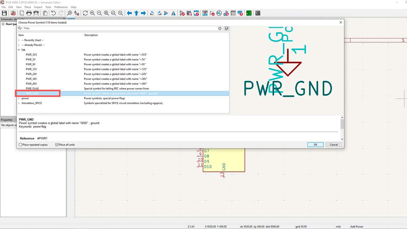
Then I began to place the symbology of the voltages that the XIAO RP2040 has, which are 3.3V, 5V and the GND and connect them in the schematic diagram to the microcontroller.
Then in the schematic design we connect the mentioned points with the XIAO and we always have to be attentive since any bad connection can affect the design and then the microcontroller.
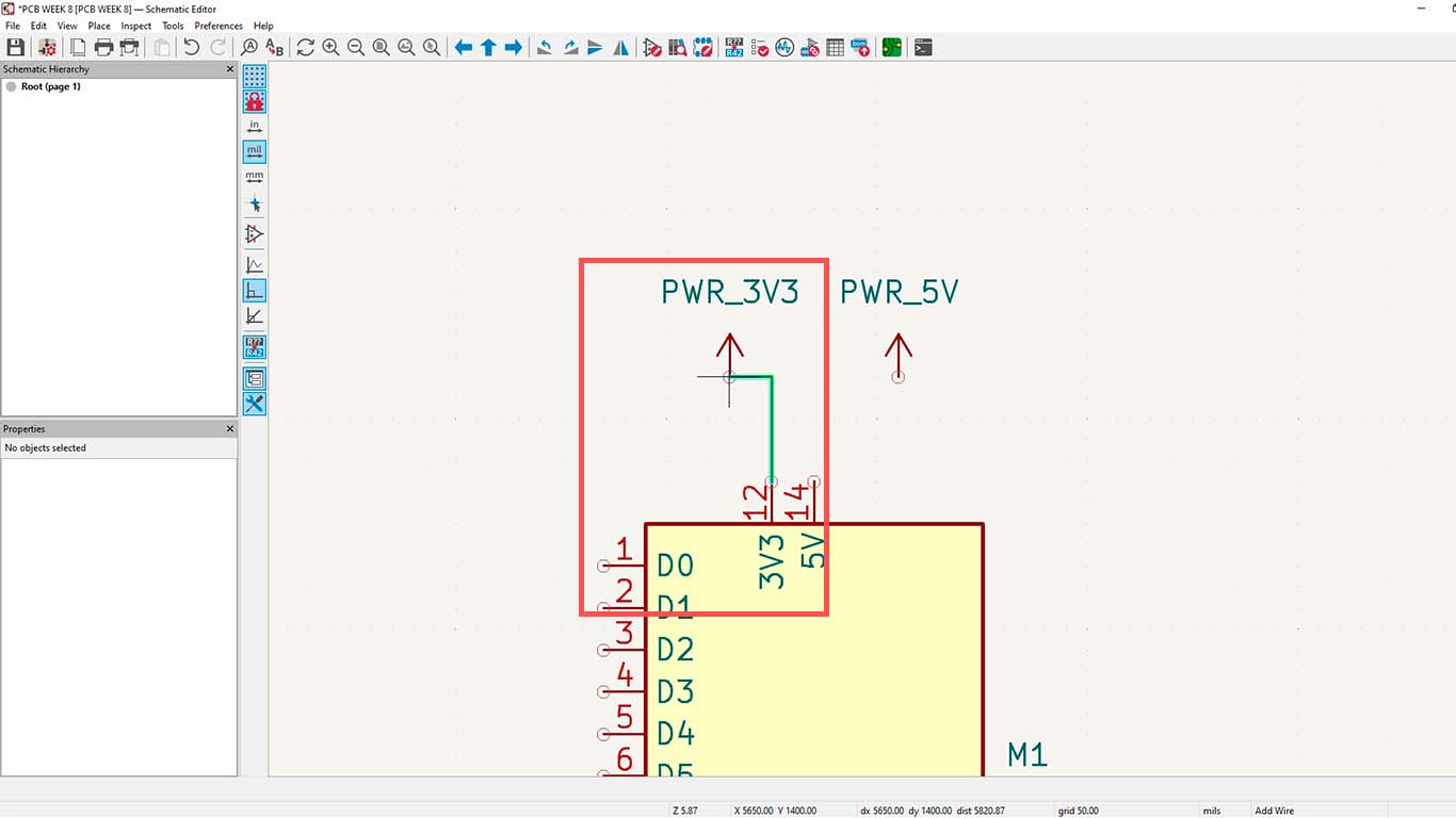
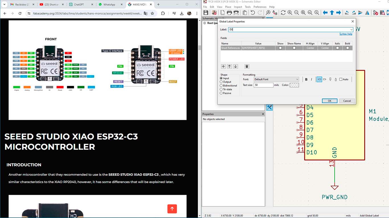
Then, we will add labels to the XIAO PINs to be able to differentiate each one of them. What I would recommend is to have the microcontroller datasheet and the KICAD next to it so that you can understand what the pins are and can guide you with it.
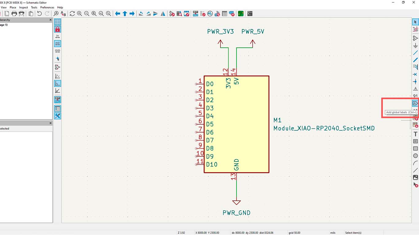
After having the pins with their labels, we must check if each one of them is correct and we can begin to develop the other components that will accompany the XIAO RP2040.
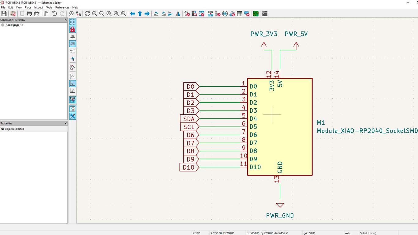
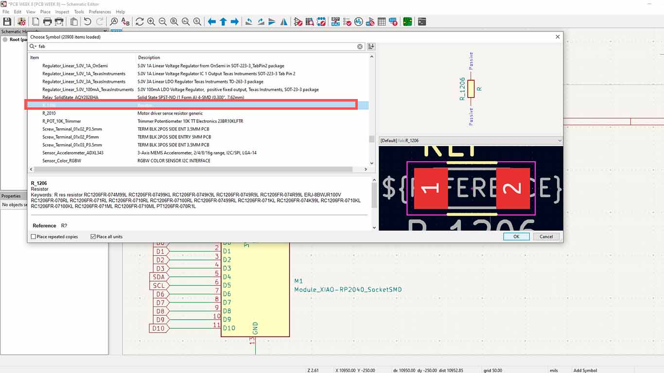
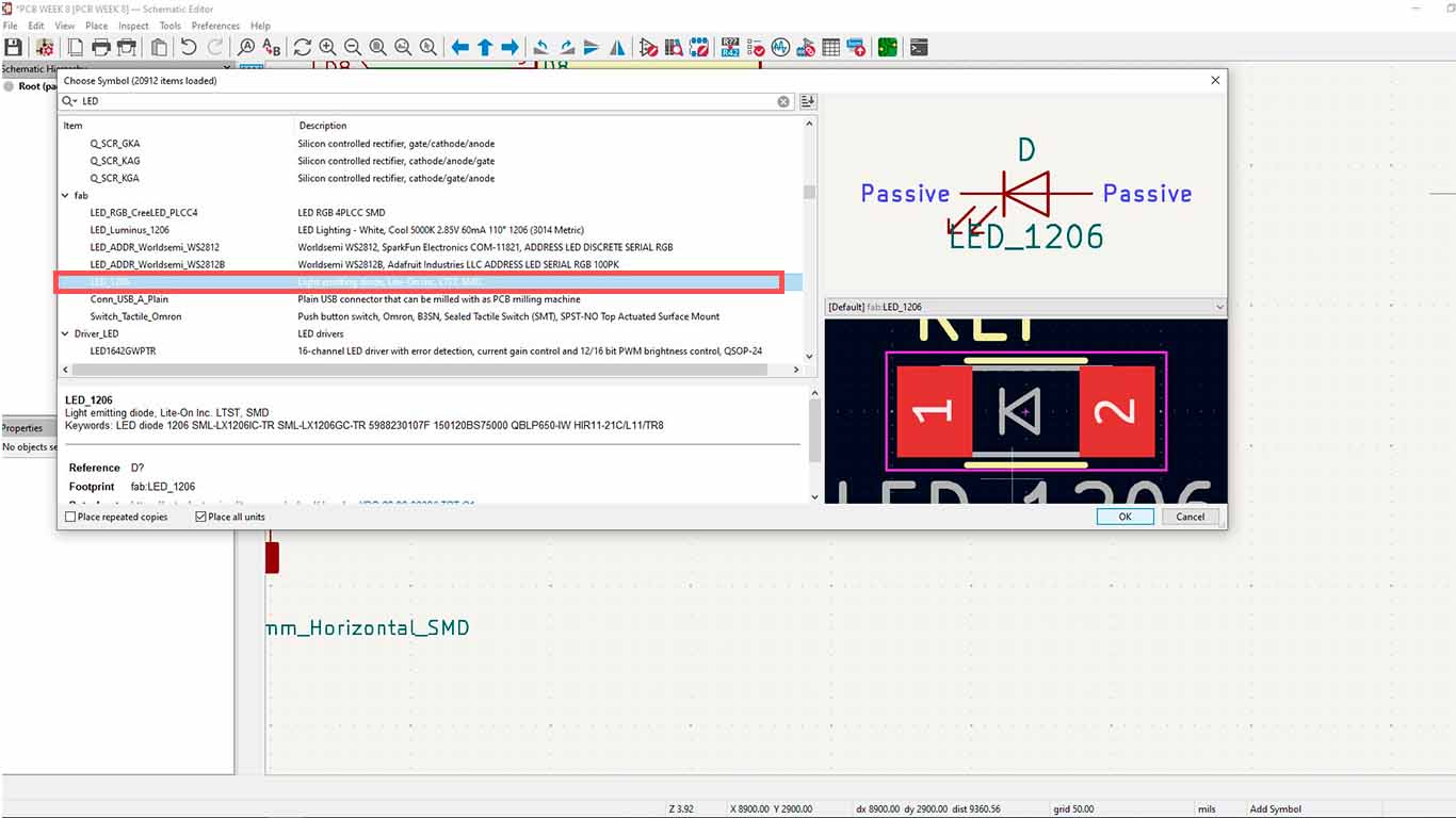
For HAPPLE we will add a touch switch which is what we have in the FAB LAB.
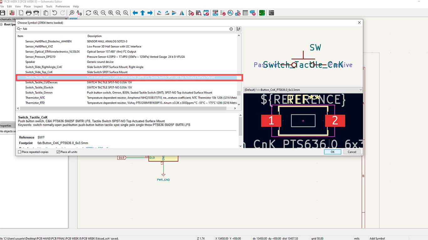
So we will also add resistors and 1206 LEDs, which are the ones used in the FAB ACADEMY. We have to look for these in the FAB library since it is important for their FOOTPRINTS and to have the right size when physically placing them and soldering them.
After adding all the components, we have to join them and form a NETWORK with each of them, always taking into account the 5V, 3.3V and GND pins for their operation. Now we will move on to the design stage, here at the top we look for the OPEN PCB EDITOR option
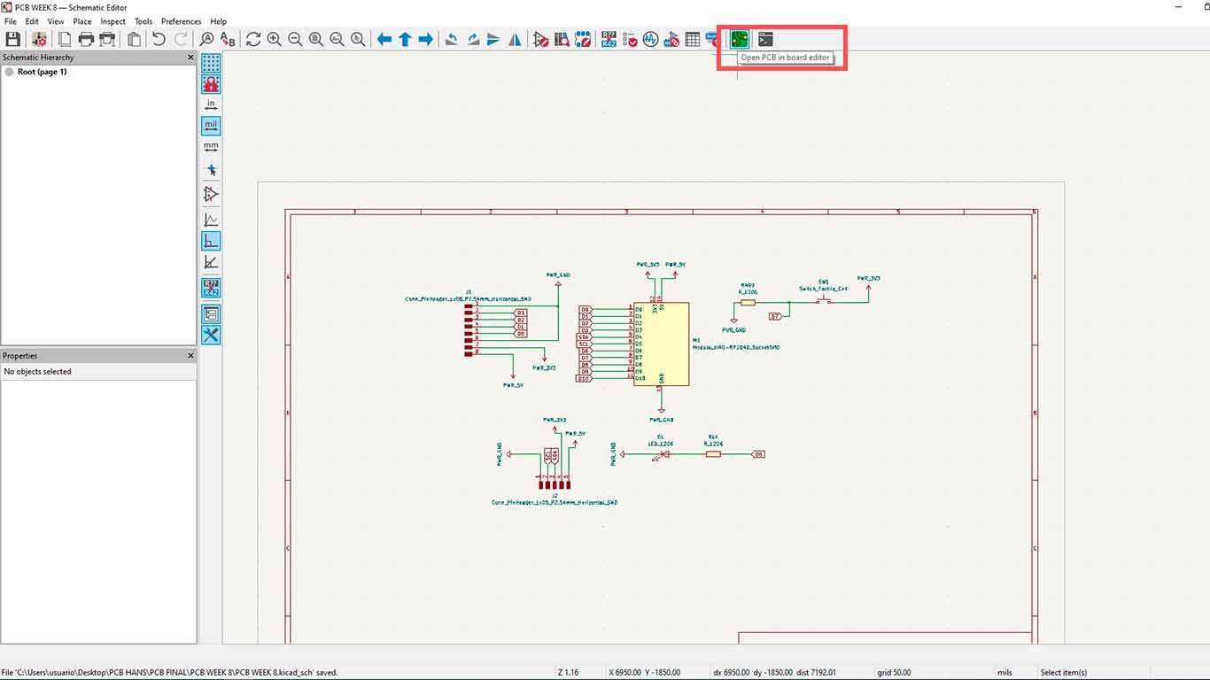
Now to bring everything worked on in the KICAD schematic area, we go to the top and look for the option UPDATE PCB WITH CHANGES, we click on it and a window will open where if we do not have an error we click on UPDATE PCB, Remember that if you have an error it must be because some component does not have its FOOTPRINT.
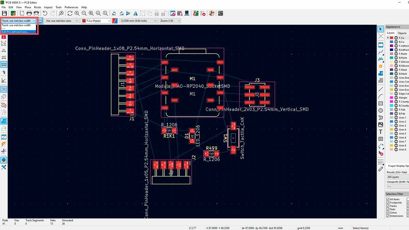
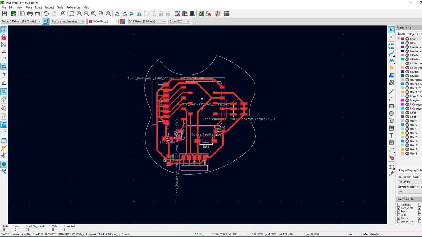
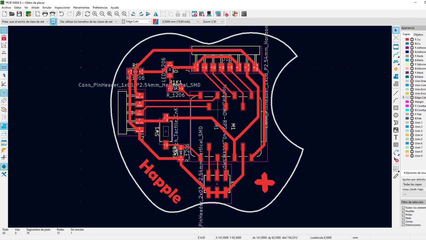
Finally, we click on the work window and all the components will be loaded, where we will begin to distribute correctly and perform the TRACES.
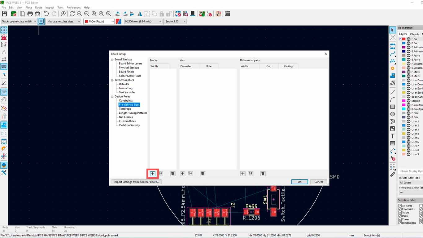
After arranging our components in the design area, we will start creating the TRACES, but first we have to configure the widths of each of them. So we will go to the upper left side in TACK and choose the last option.
In the new window we go to the bottom and look for the + sign that will allow us to add the widths of the traces.
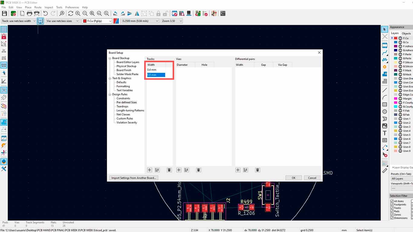
For my plate I chose 2 types of widths. The first 0.8 mm for the 5V, 3.3V and GND pins since it is important to carry the power and finally for the other 0.4 mm pins.
Finally, after a little stress I managed to fit all the tracks and it seems to me that it is ready for milling.
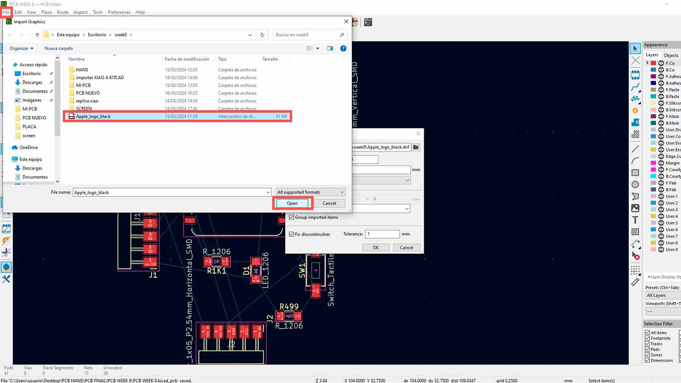
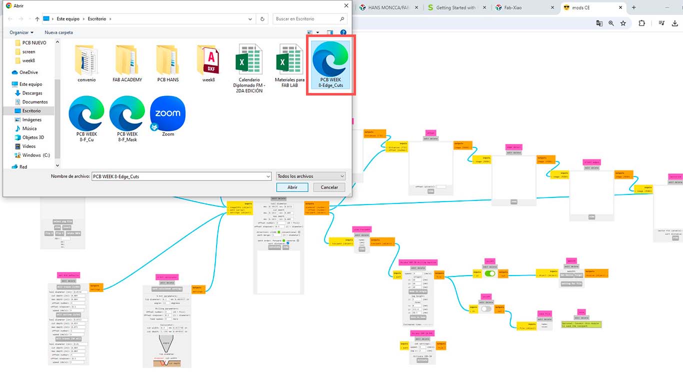
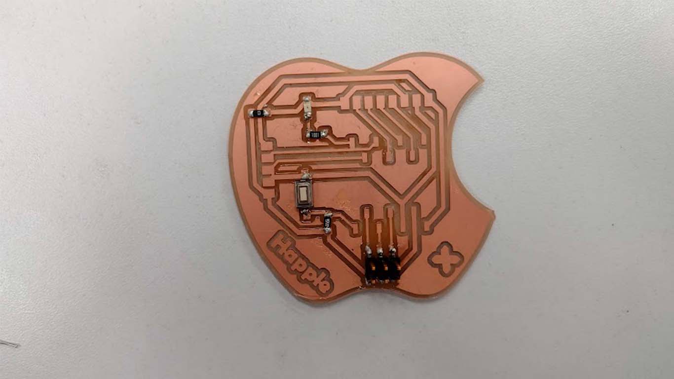
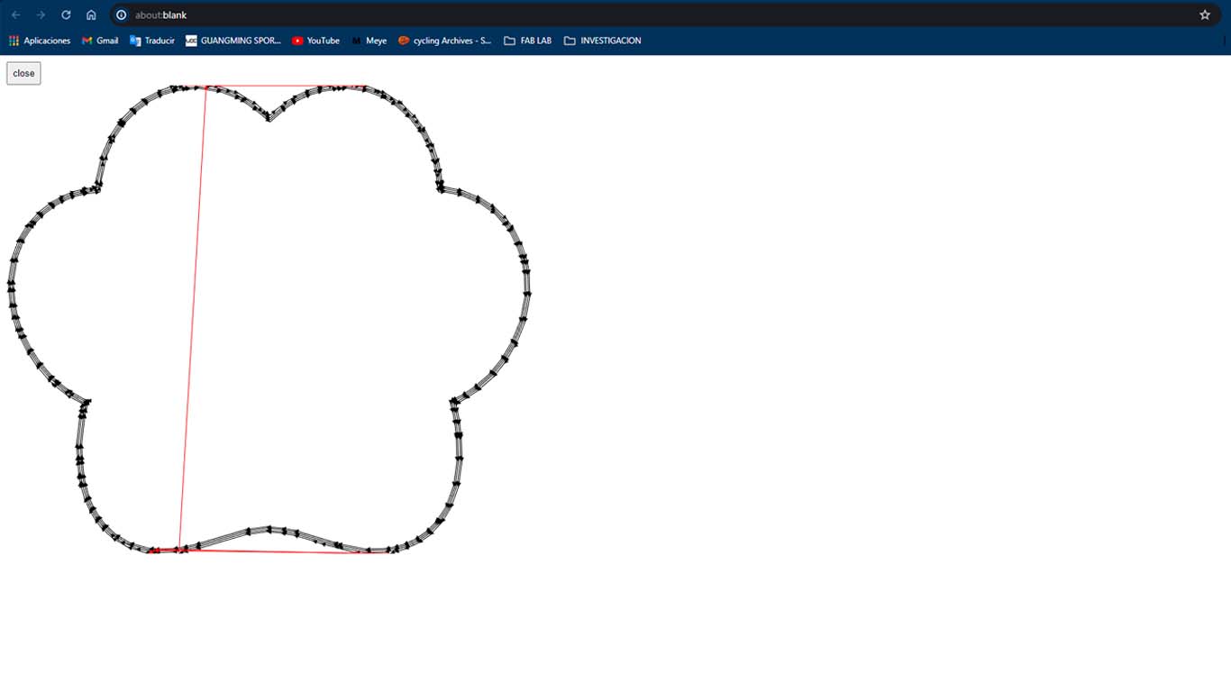
To bring any design that we want to give to our board we have to have it in DXF since another type of file worked for me. We go to the FILE / IMPORT tab and here we choose the file we want to bring, in my case the apple. Then we have to choose the EDGE CUTS layer since it is the layer that is intended to shape the plate.
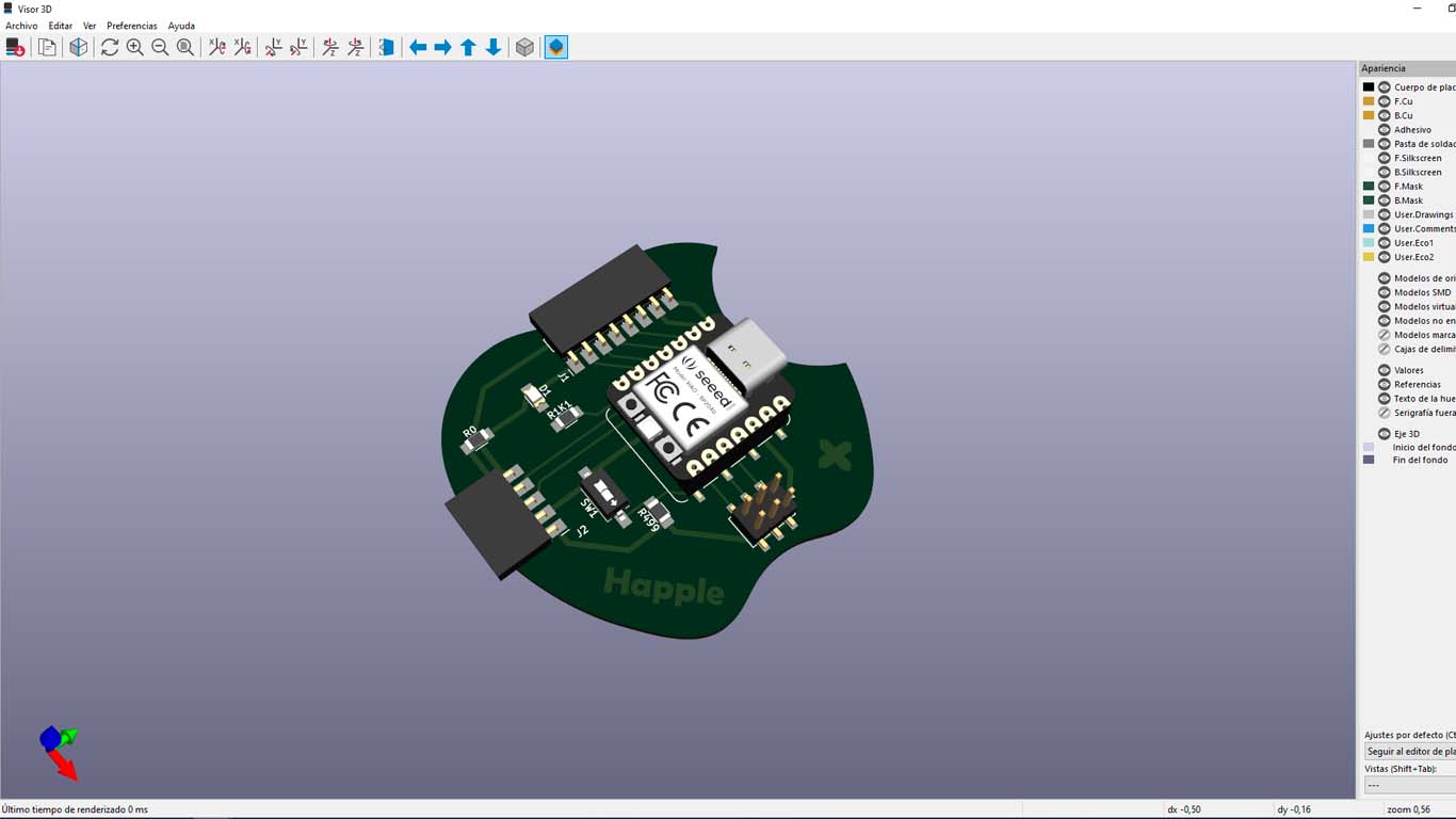
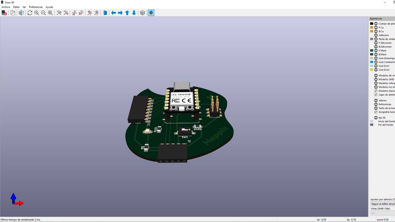
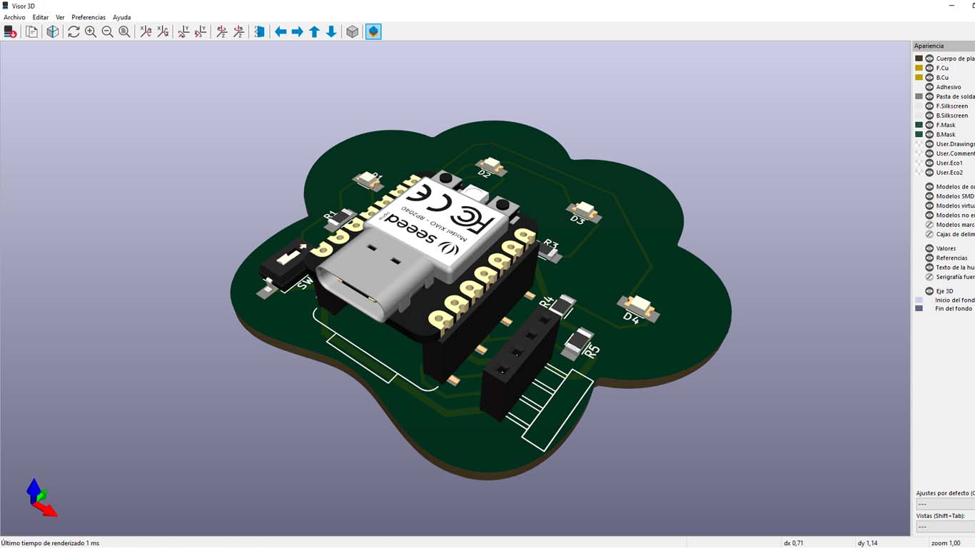
Here I show you a 3D capture of my board in KICAD. After a review of the components and traces, we will proceed to milling it.
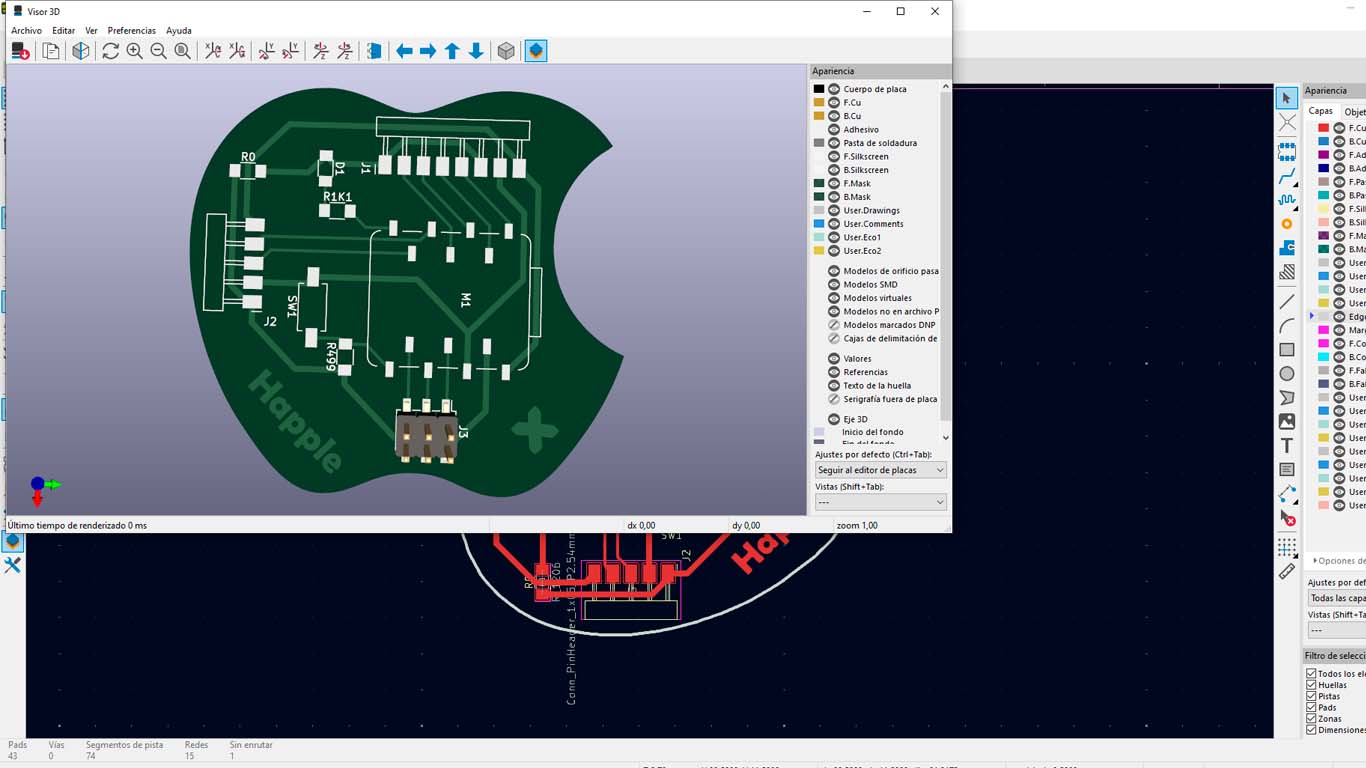
For the 3D in Kicad, I added the 3D models that KICAD had for each component and then downloaded from other pages that the FAB ACADEMY recommends for each component. Here an example.
MAKING HAPPLE X
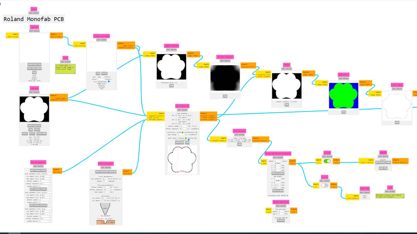
EXPORT TO MODS CE
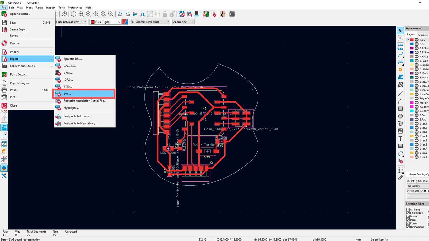
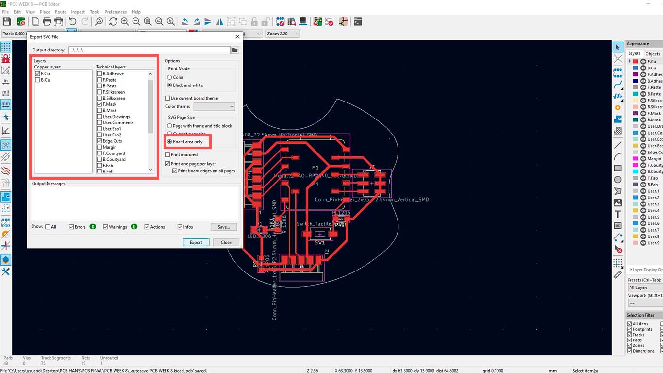
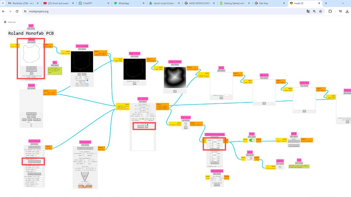
In order to send the made plate to be milled we have to export it to MODS.CE, for this it is important to have the plate in PNG or SVG. Therefore, first we will export from KICAD to SVG by entering FILE/EXPORT/SVG. Here a window will appear where we will activate the options according to the 2nd image and export.
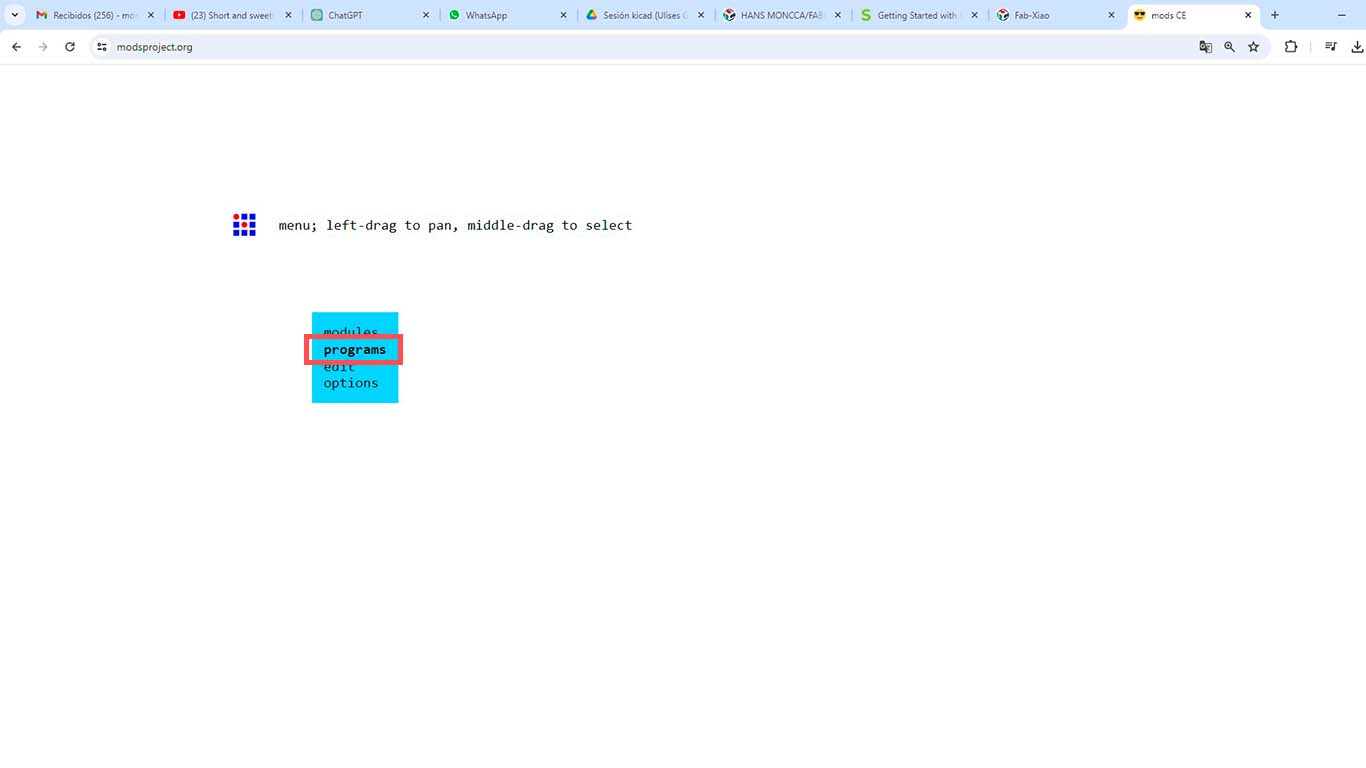
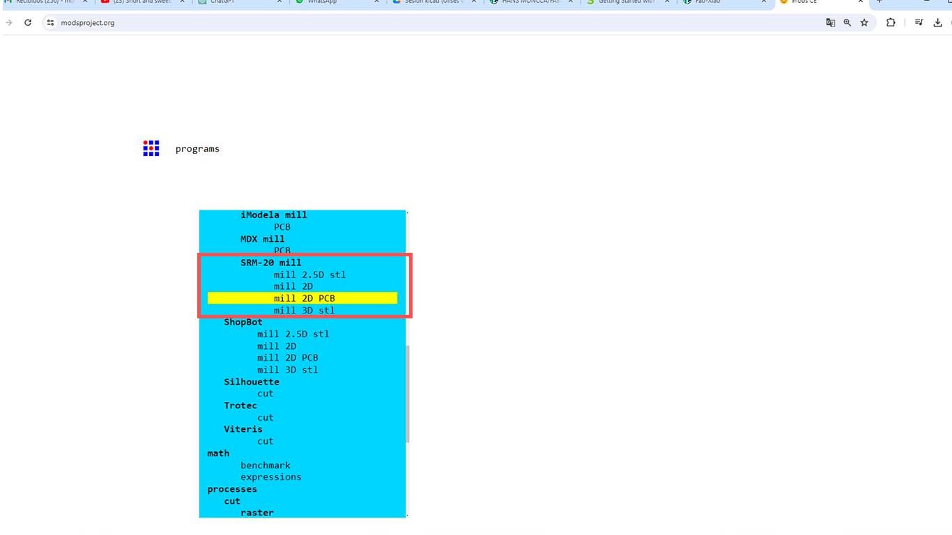
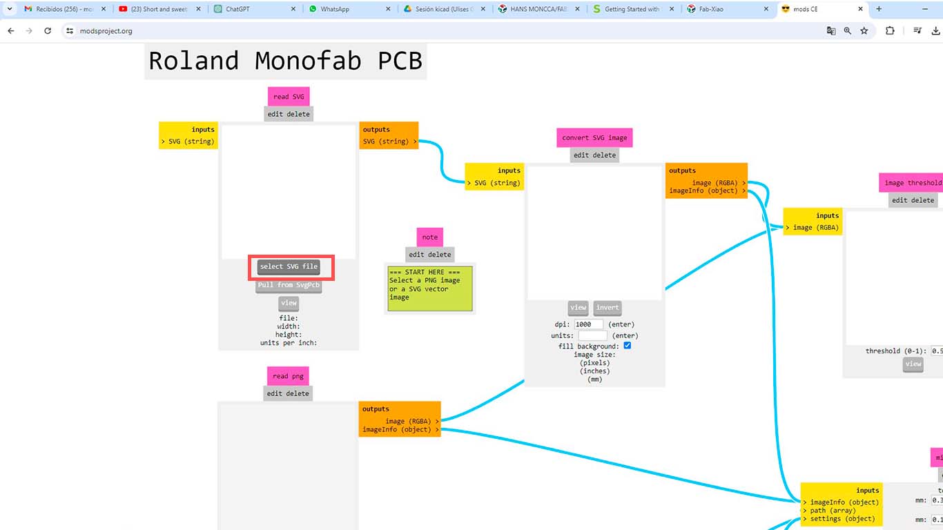
After obtaining both SVGs, we go to our browser and look for the MODS.CE page, where we will click on PROGRAMS, from there we look for our milling machine, which in my case is the SRM20.
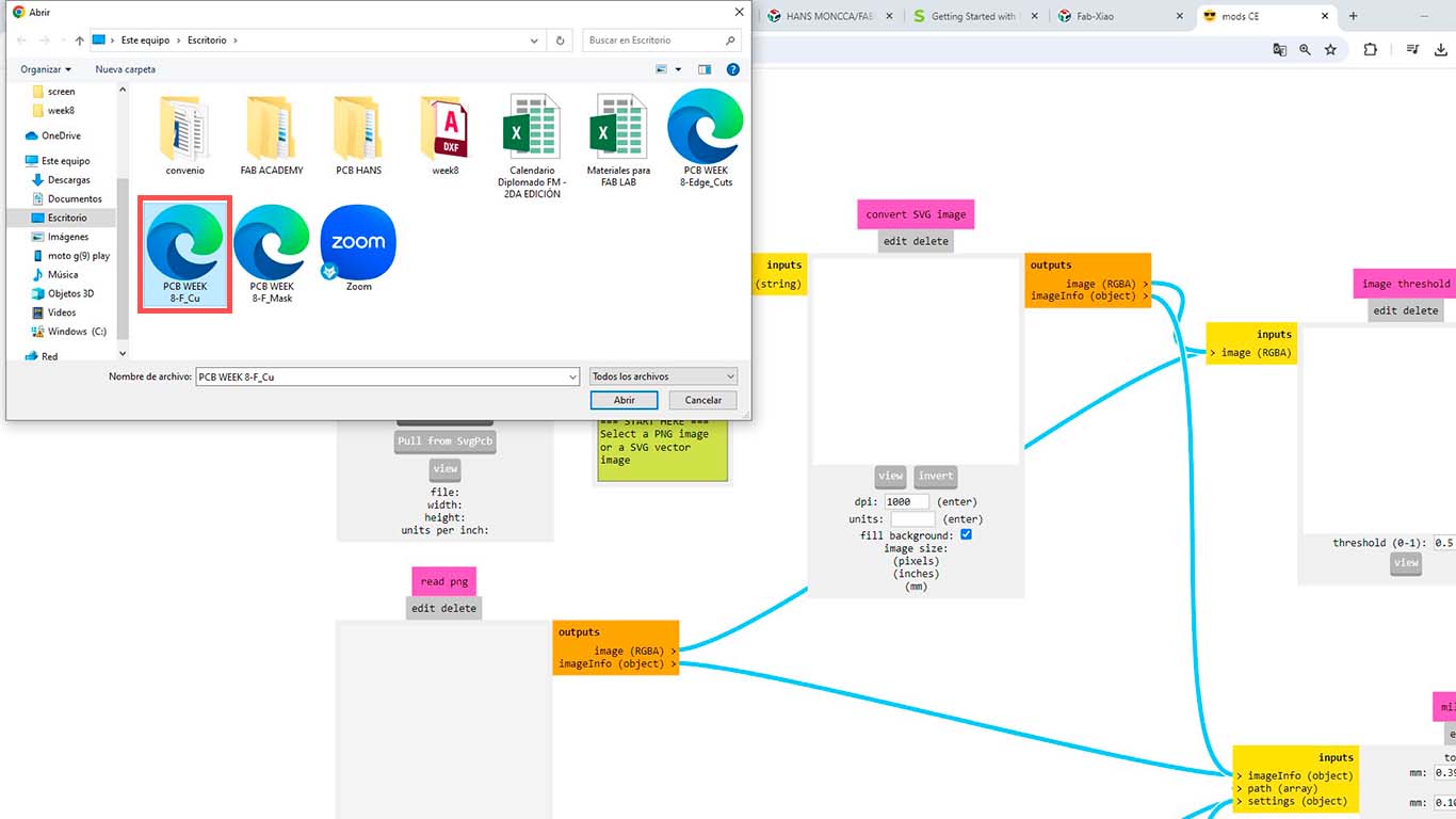
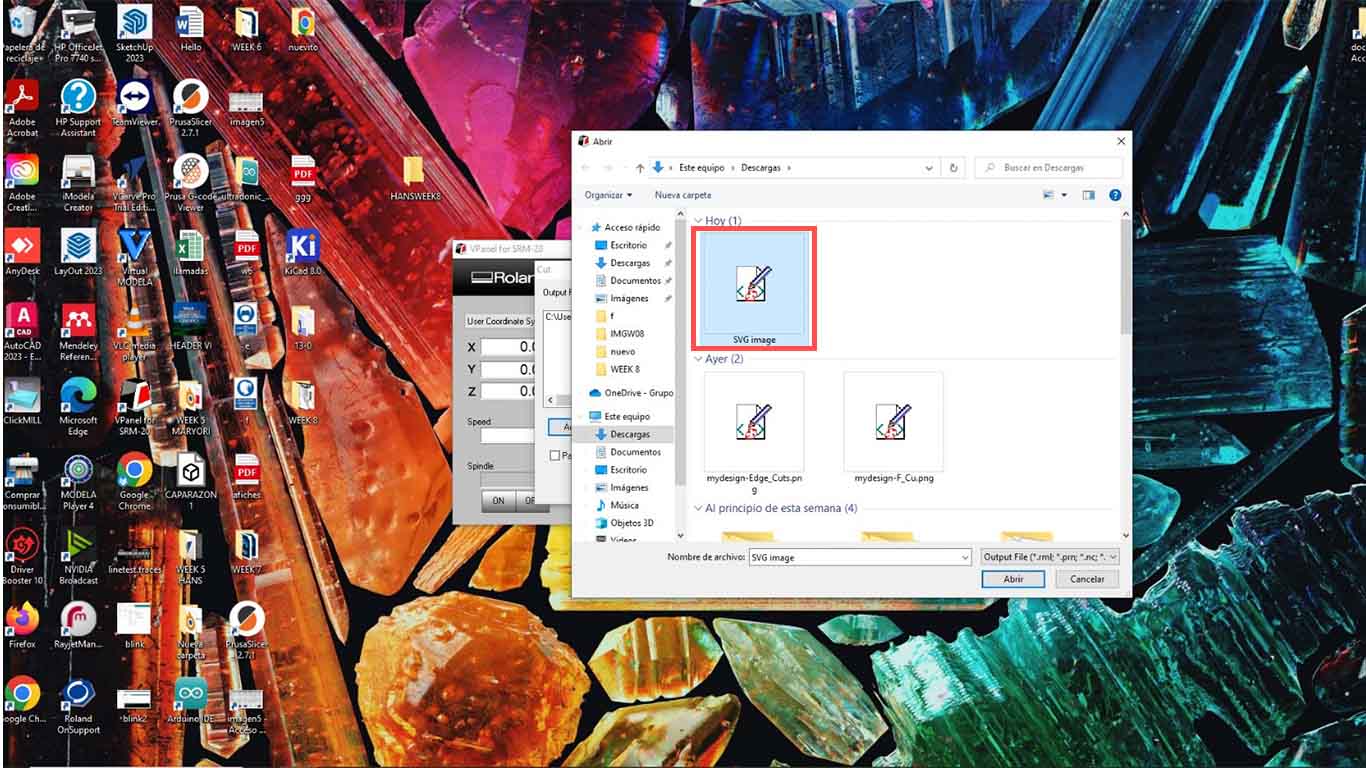
In my case, I have my file in SVG, so we click on SVG FILE, we search on our computer where we export the files of our layer and we choose the TRACES file first.
Then we click on INVERT since in order for MODS CE to make our board we must have it negative and our tracks and footprints blank. And let's not forget to press the WILL TRACES 1/64 since it is the measurement of the milling cutter that is used to make the traces.
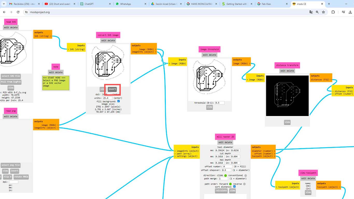
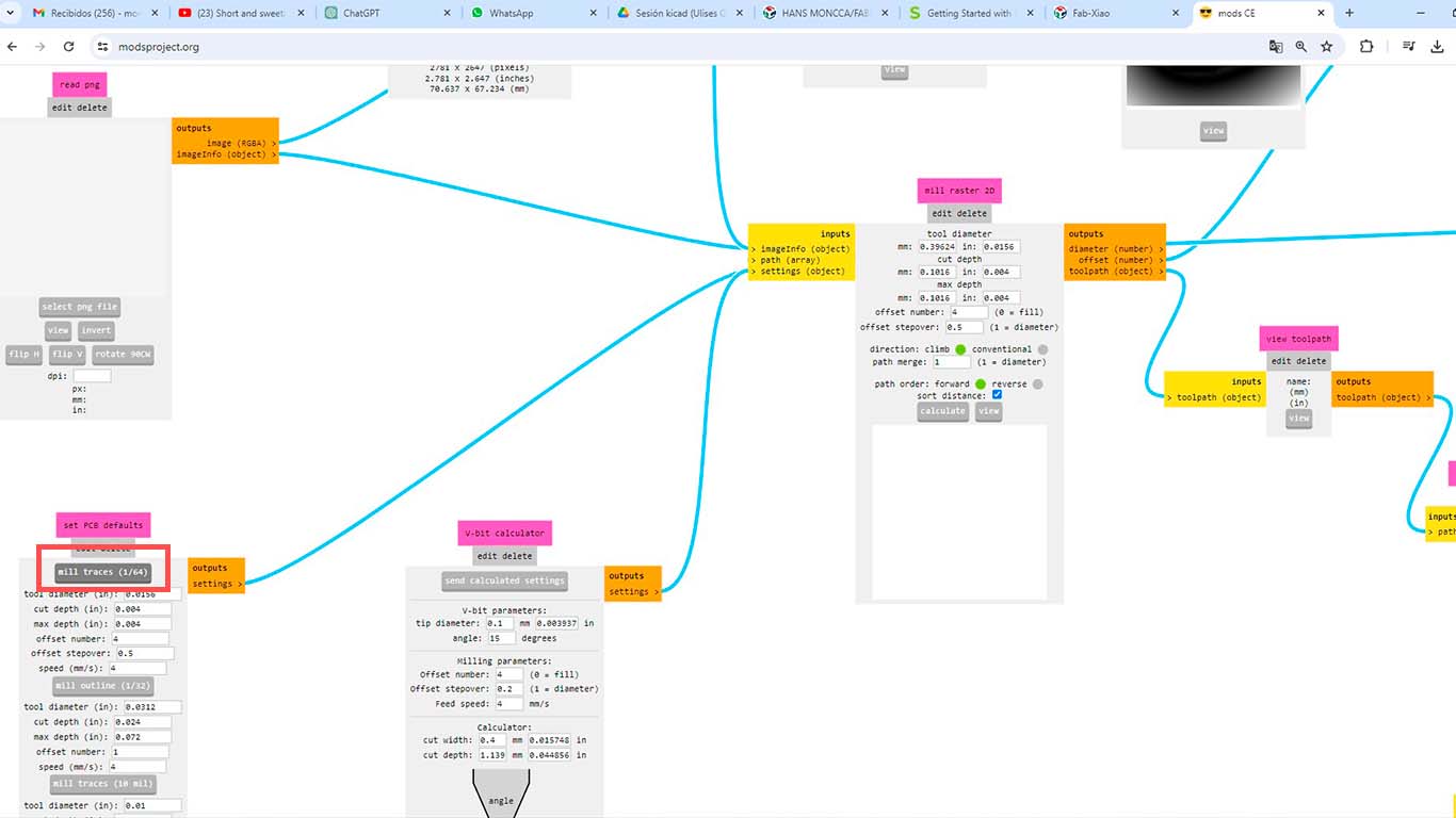
After doing all of the above, we click on calculate and the MODS will give us a preview of the work it will do, let's check if everything is okay.
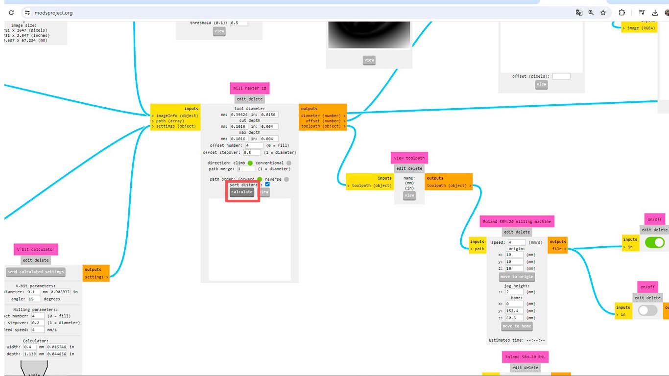
Let's not forget to change the X, Y and Z axes to 0 so that the machine can mill where we physically calibrate it.
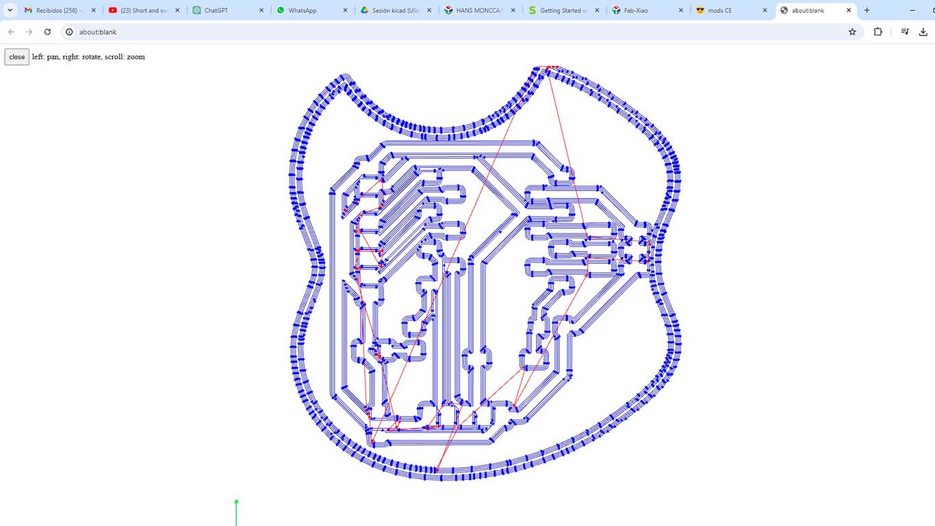
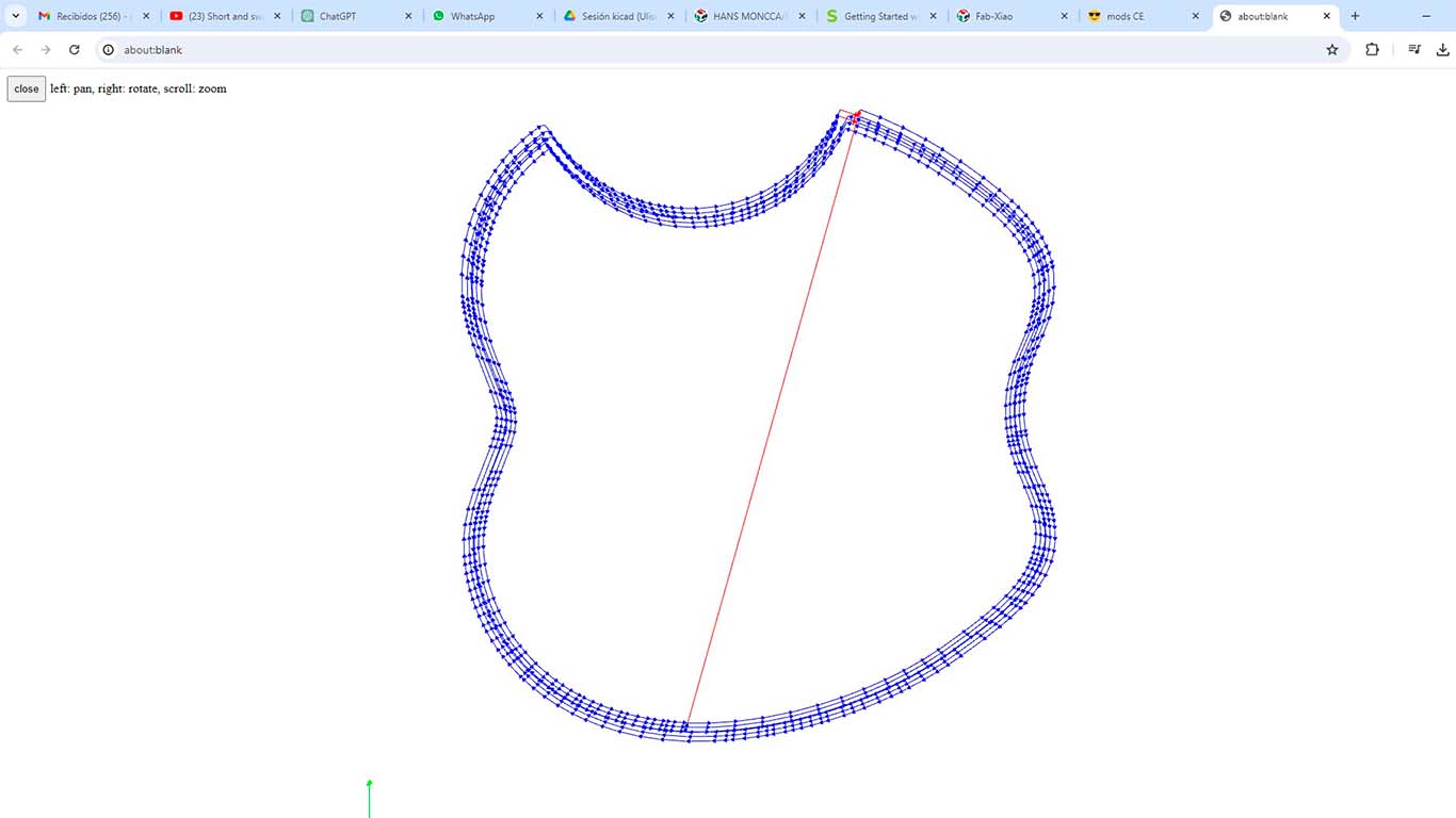
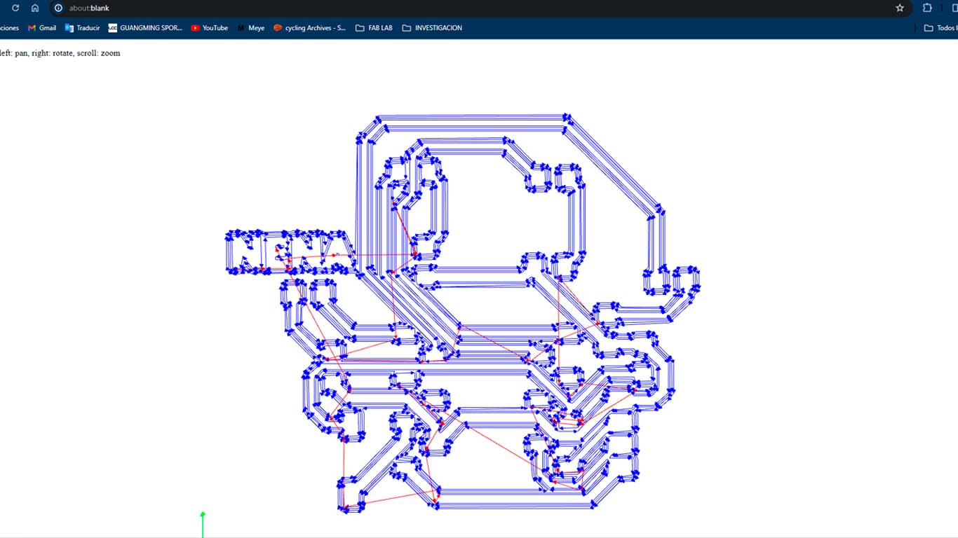
And finally we get a preview of the milling path and we can download the file to import it into the ROLAND software.
We will do the same steps with the edge of the plate, this time we will first look for the file that we exported from KICAD and upload it to the mods.
After uploading, we have to change the milling size, in this case it is 1/32, then we change the data of the X, Y and Z axes to 0 and finally we click on calculate and we obtain a preview of the job and download it.
Finally, we are ready to mill my new development board.
MILLING MY BOARD
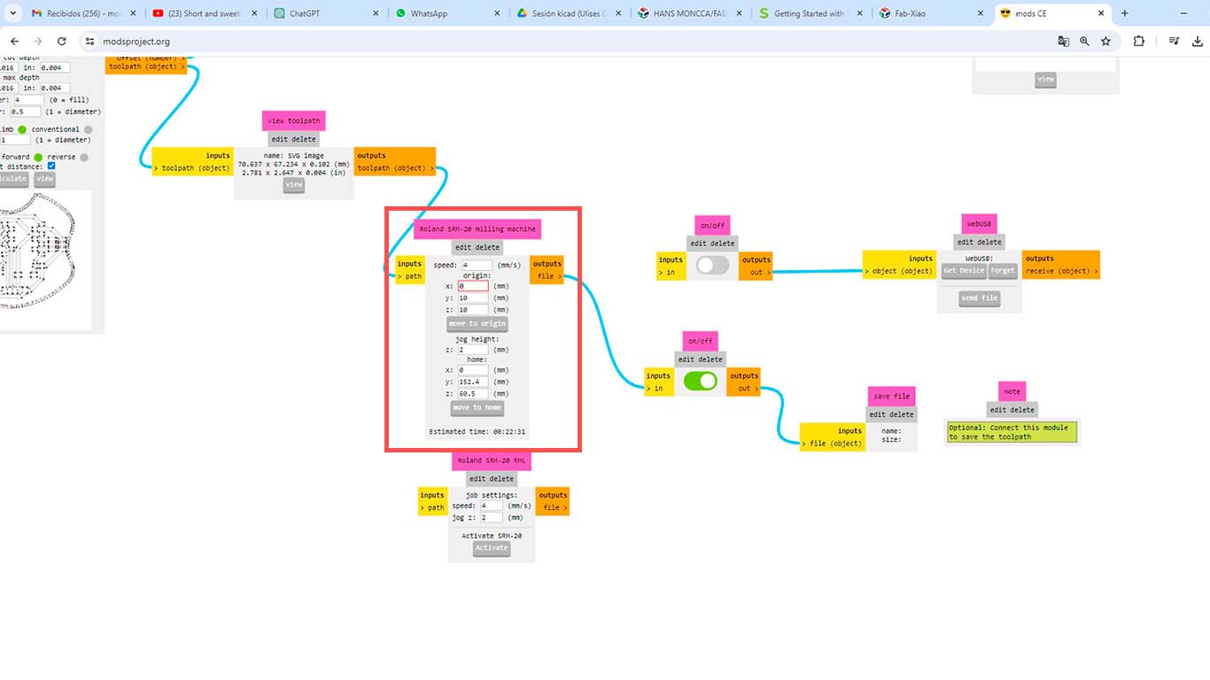
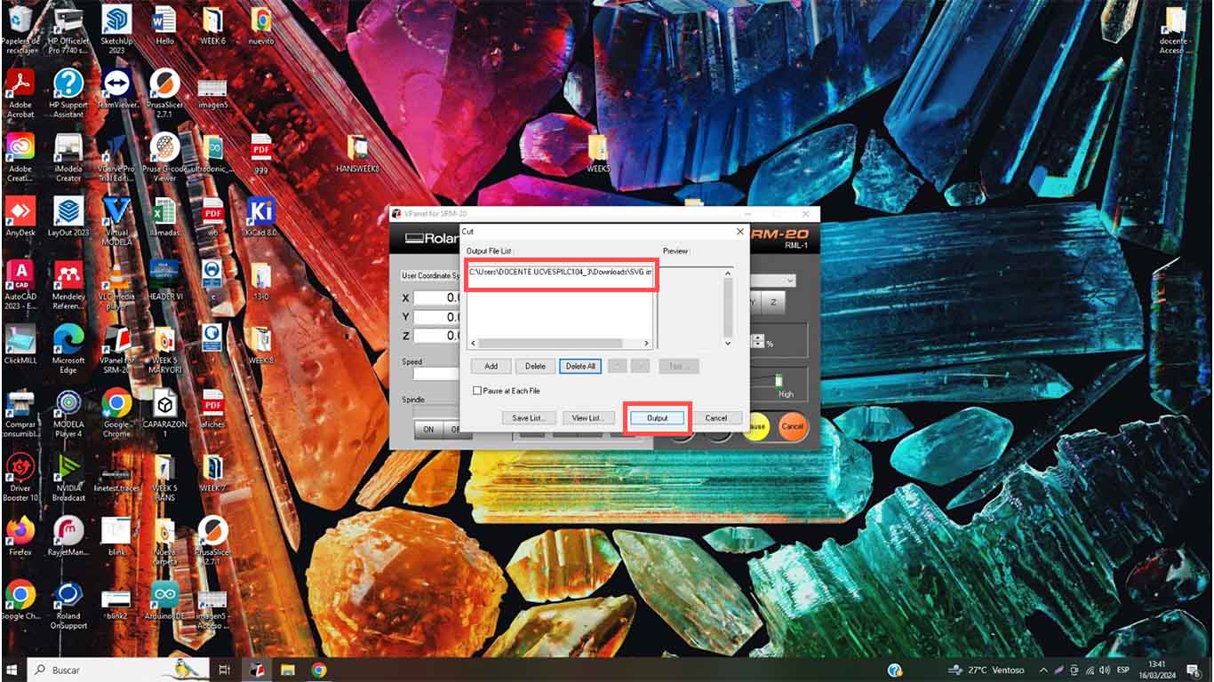
After obtaining the files to mill, we export it to the ROLAND SRM 20 program where we look for the file where we saved it and open it with the software.
Then we check that it is the correct file, we load it and click on the OUTPUT button. Let's remember that before carrying out this process, we have to calibrate the machine in its 3 axes.
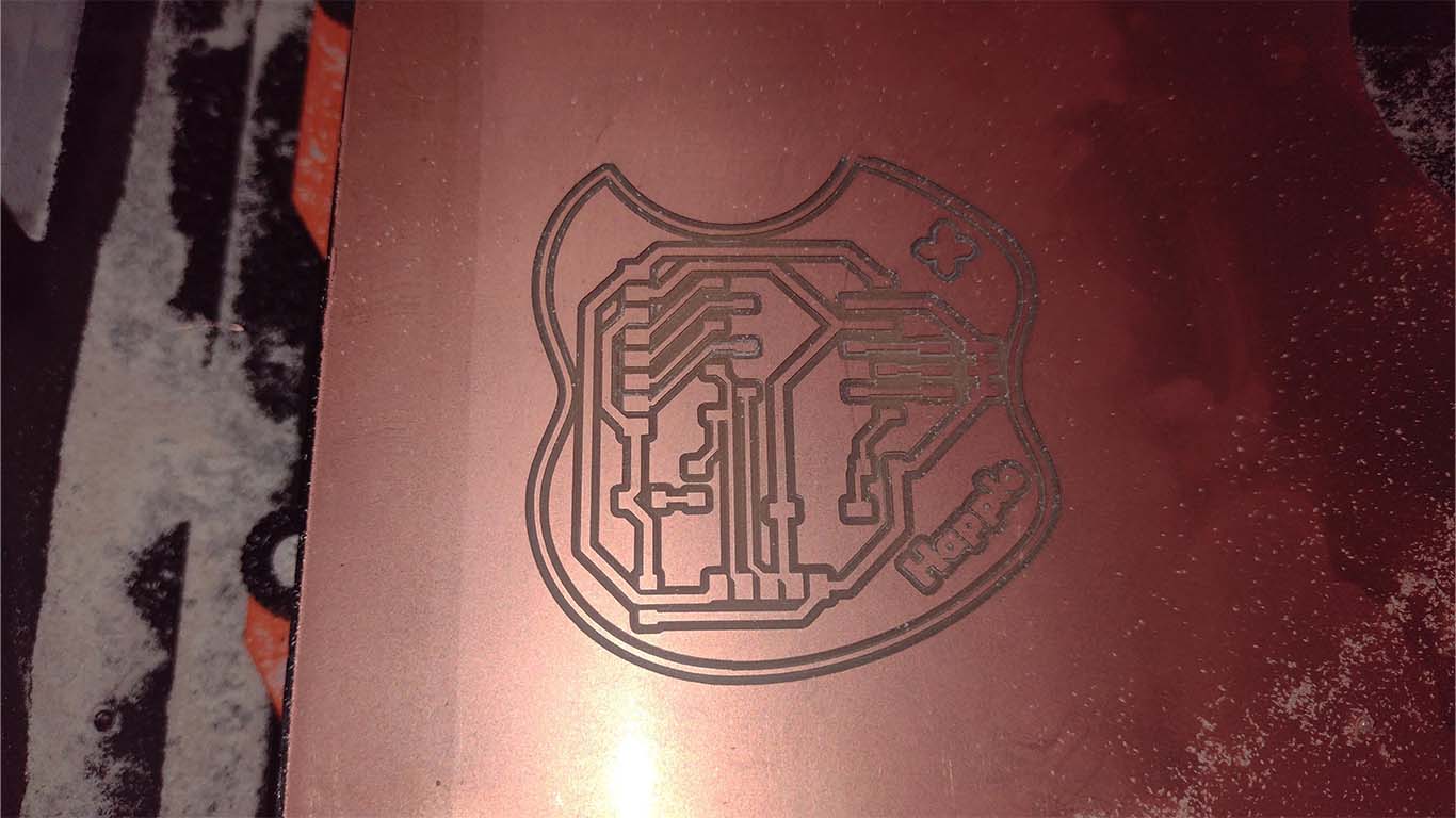
Here are a couple of videos of the HAPPLE X milling and then proceed to welding.
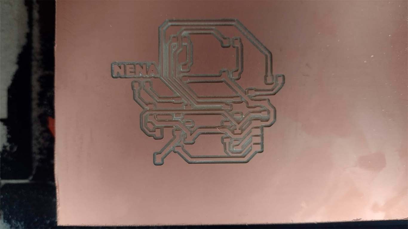
After the milling process, here are some photographs of the result, I see that the traces and spaces of the components came out very well.
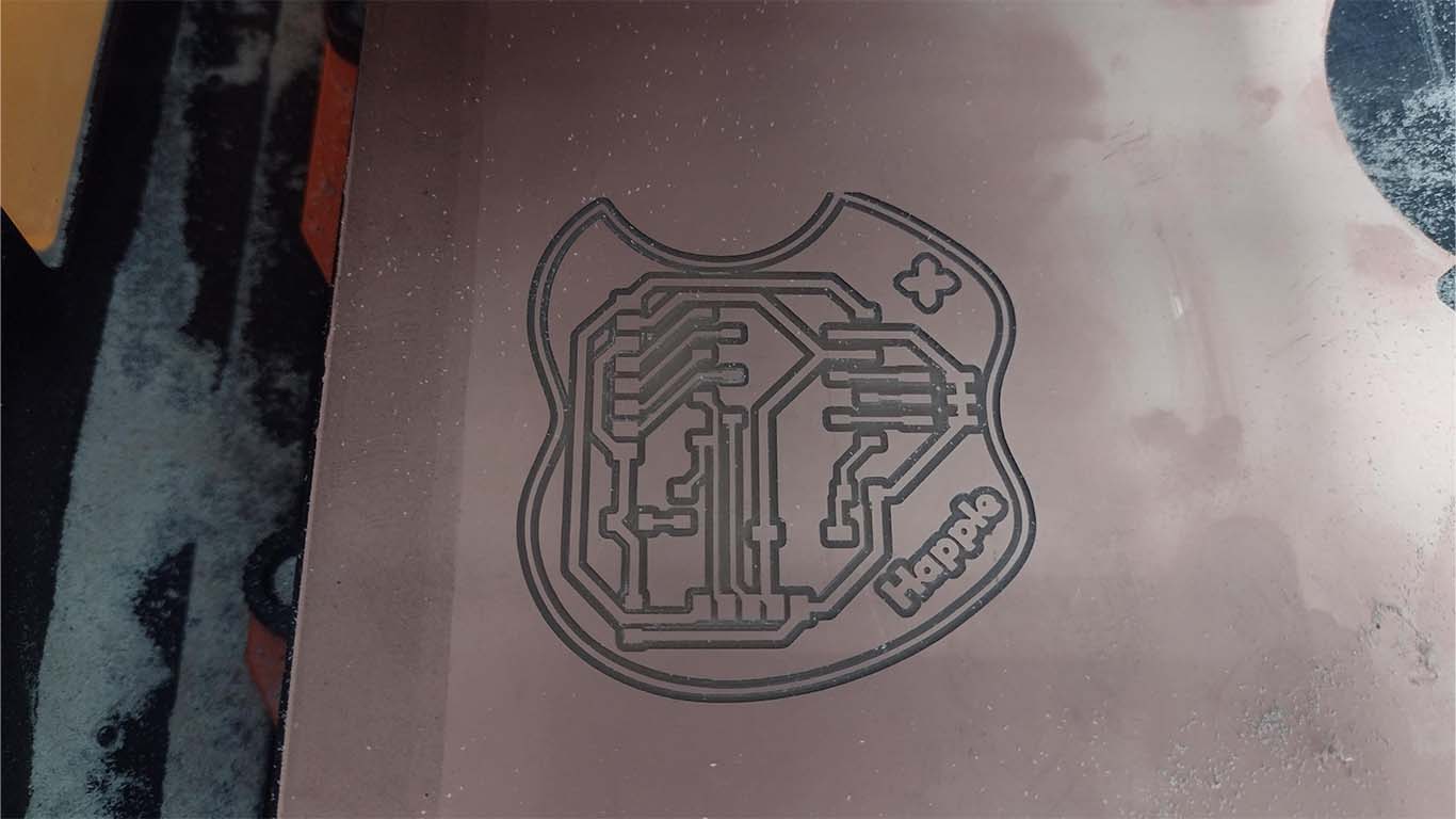
And finally, I had it cut with the 1/32 milling cutter and we obtained the development board I wanted. Now I will show the component soldering process.
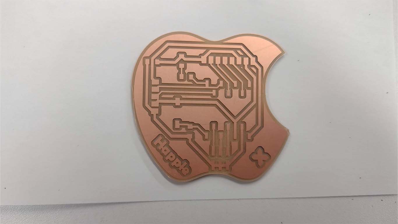
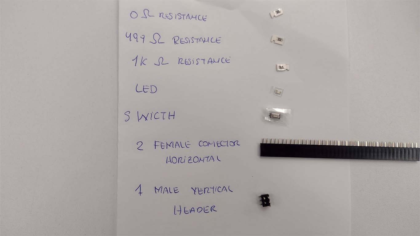
COMPONENTS
Here is a list of the components that I am going to use on my development board.
| RESISTANCE: | 0; 499; 1K Ω |
|---|---|
| LED: | LED SMD RED |
| SWITCH: | SWITCH TACTILE |
| CONNECTOR: | 2 FEMALE CONNECTOR OF 8 AND 5 PINS |
| HEADER: | VERTICAL HEADER OF 6 PINS |
| MICROCONTROLLER: | XIAO RP2040 |
Here I show a photograph of the components that I used to make my development board.
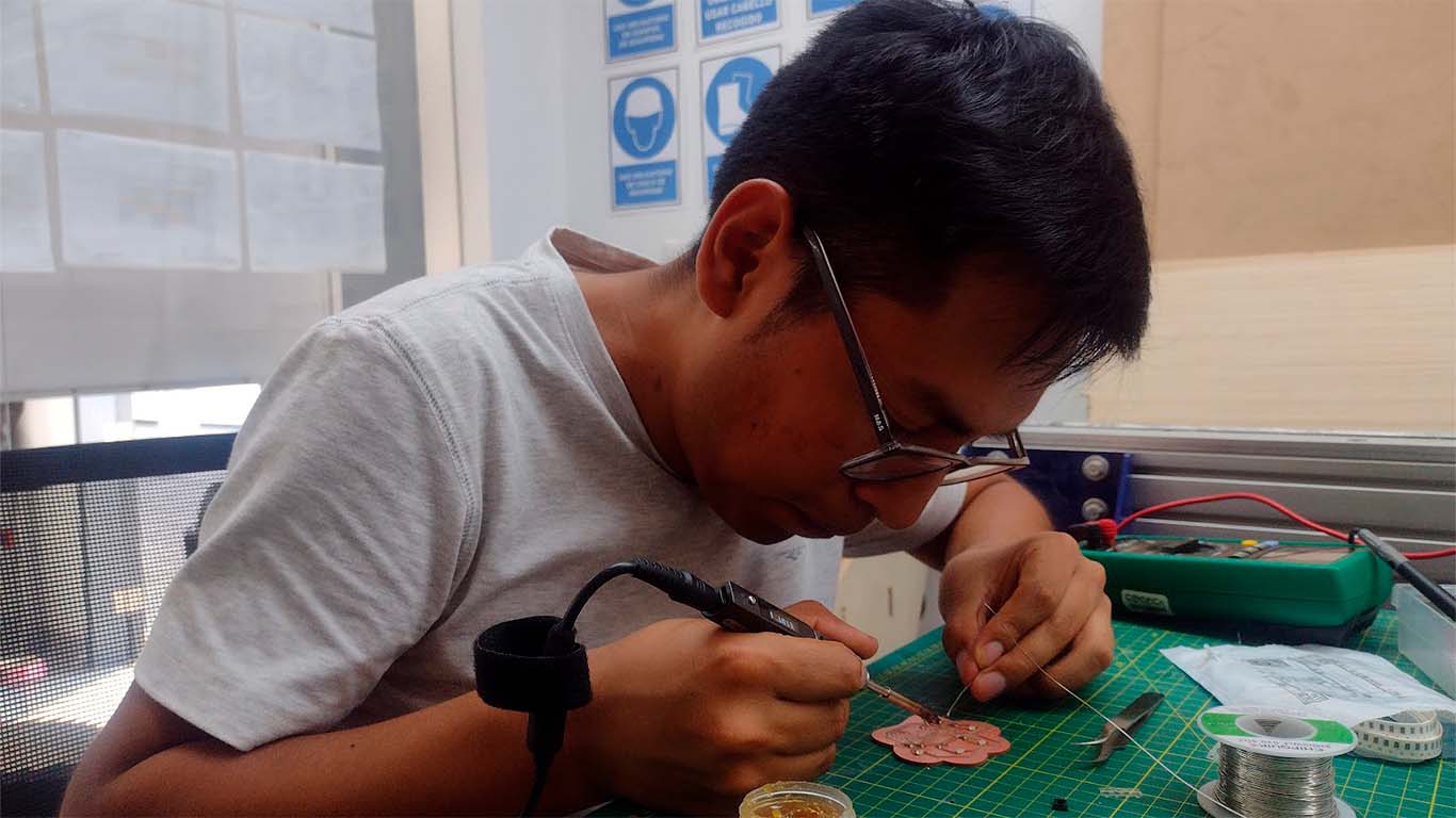
SOLDERING MY BOARD
For the soldering process of the components mentioned above, I first started to solder the components that are more difficult for me such as the HEADER connector, RESISTORS, THE SWITCH AND THE LED, this because they are very small and we have to be careful with them when time to solder to avoid making a short circuit and the soldering has to be precise, neither too much nor too little because they must maintain the continuity of the tracks.
Then I soldered the 2 female connectors that will be where the pins are connected for programming inputs and outputs.
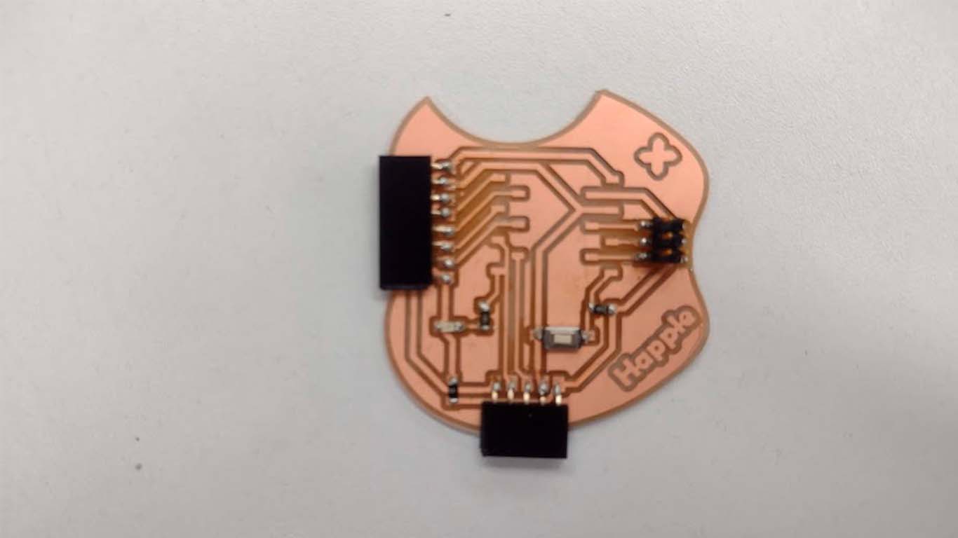
Then I also soldered 2 more female connectors to receive the XIAO RP2040 since I only have 1 microcontroller and I need to be disassembling it to change it both on this new board and on the QUENTORRES, done during the ELECTRONIC PRODUCTION week.
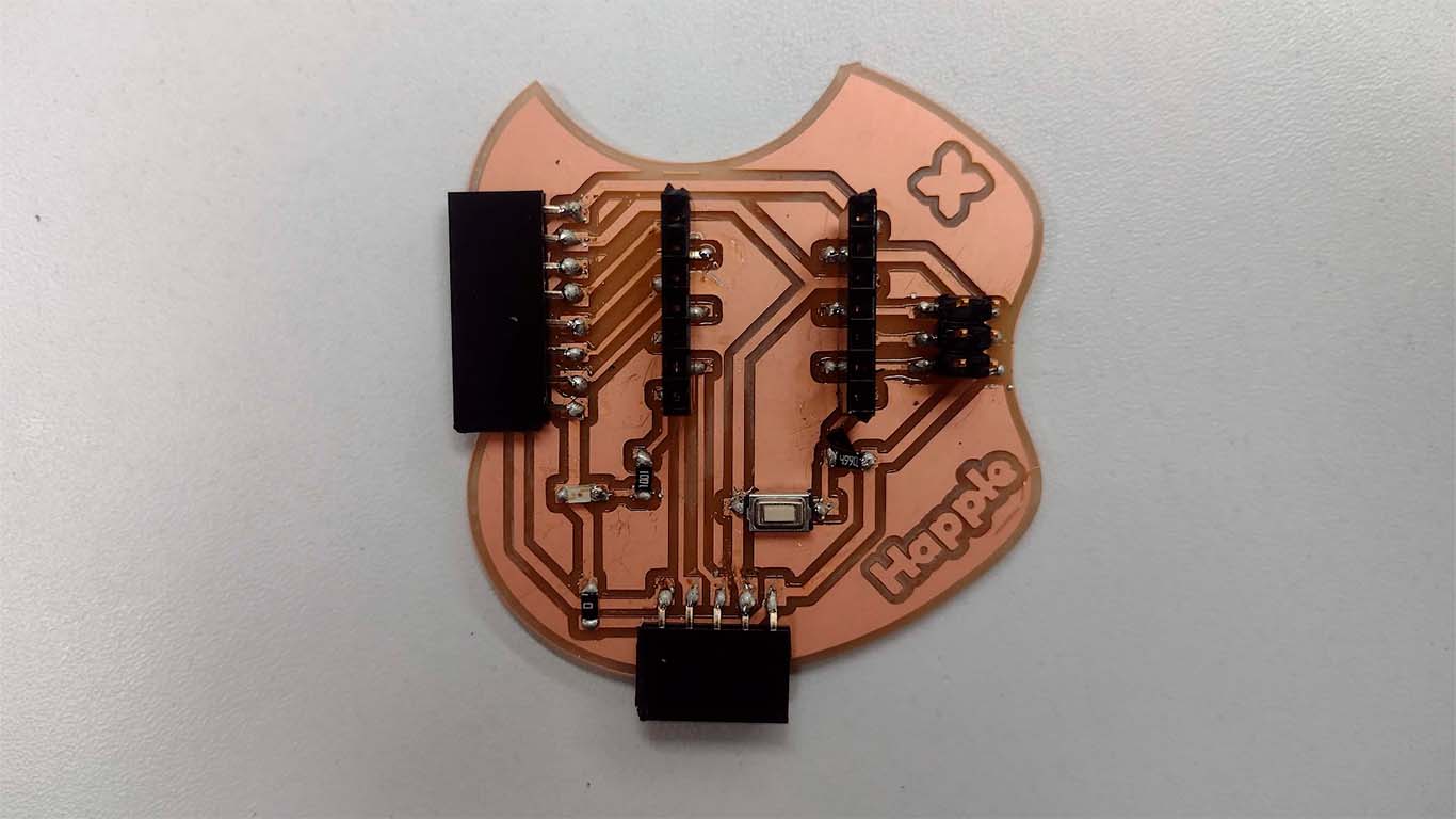
Finally, once everything has been soldered, I place the XIAO RP2040 microcontroller to move on to the input and output programming phase. Let's remember that first of all, we must check the continuity of the components to avoid problems.
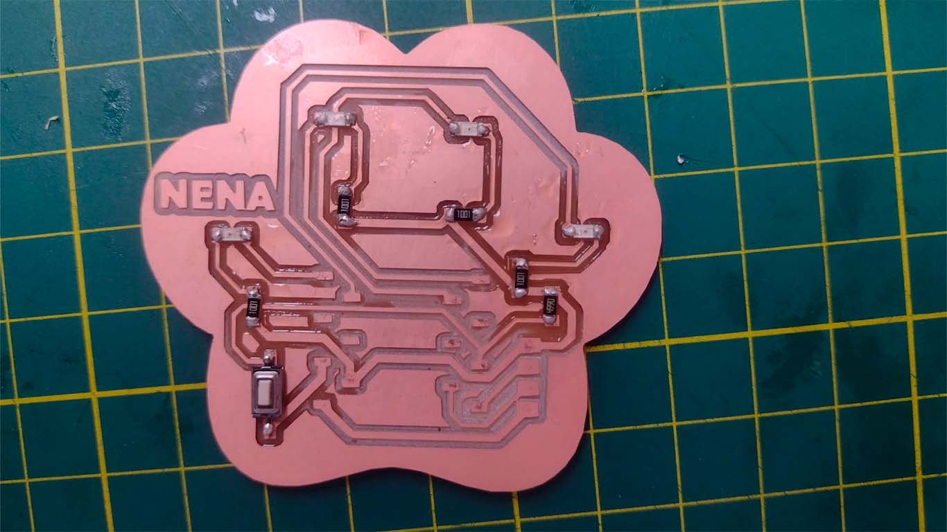
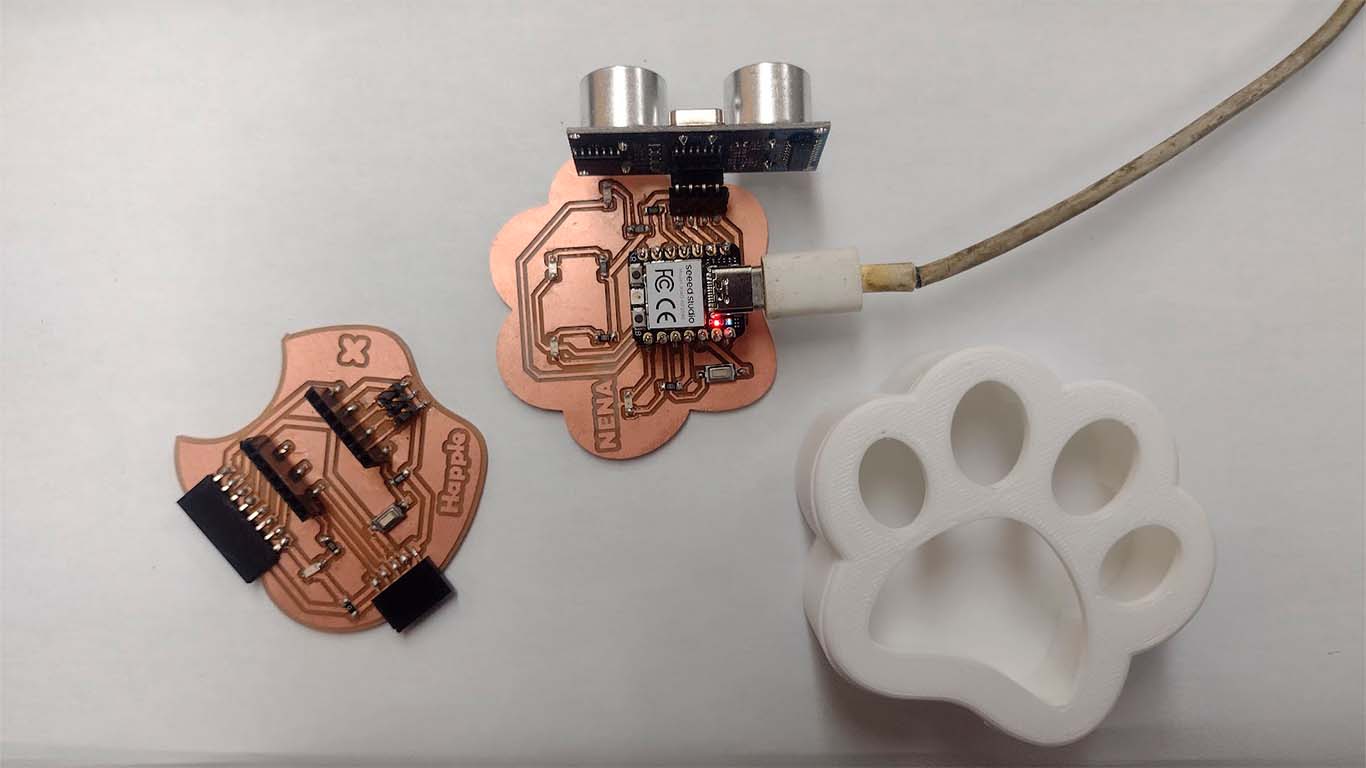
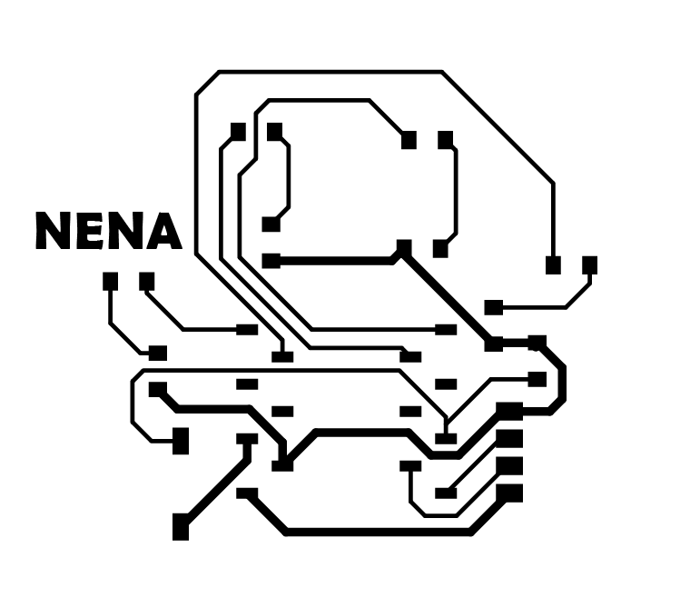
DESIGN 2: NENA BOARD
NENA: INTERACTIVE BOARD
By making my development board I understood many functions of the components, how it is assembled and how it could work. This week was hard for me, I lost my partner who accompanied me throughout my university years and her day came on Sunday. Her name was NENA, my dog, and when she came home she was always happy and wagging her tail. She was very sentimental, because when I had to leave, she got sad and when I traveled she didn't even eat sometimes. Sad for her, I decided to make a design that reminds me of her.
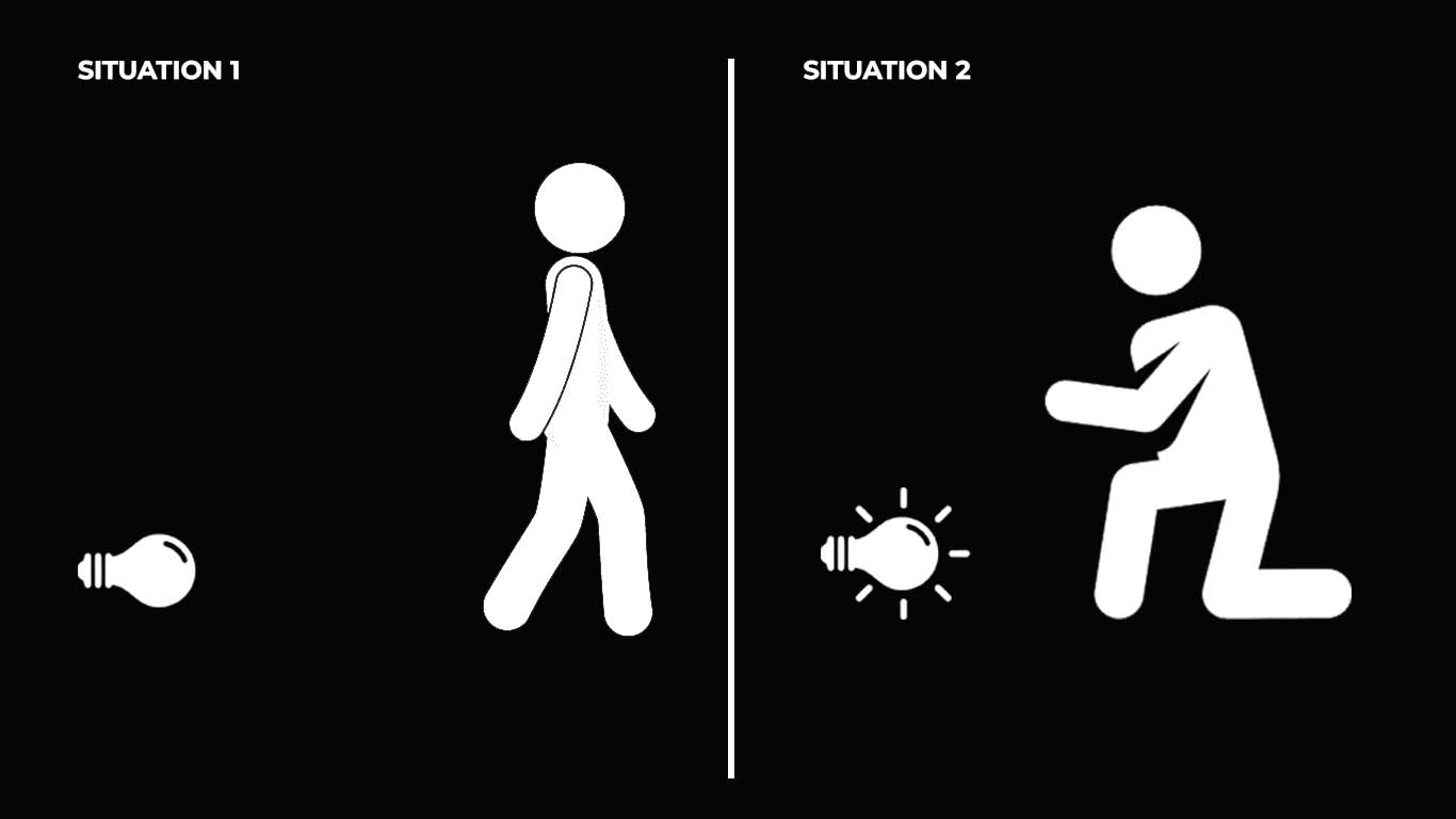
My inspiration for making this plaque was to challenge myself and show a little of the meaning of what my dog meant. The central idea was to achieve a plaque that when someone or something approached, all the lights would turn on, but the further you went, the lights would turn off up to a certain distance. And this shows a little how my dog was with me, when she was with me she shined, she was happy, but when I left she remained sad and dull. I wanted to achieve this analogy on the plate and I hope to achieve it. Here I show you the process and I did it with a lot of feeling.
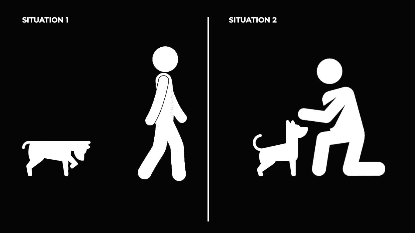
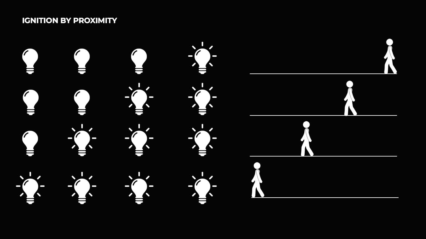
Here I show an example of the idea I want my board to do. When something approaches it, it lights up and since it has several LEDs, the idea is that it lights up one by one until all of them are lit when a person or object is close to the plate. However, if we have nothing nearby, the LEDs are off and if you feel something approaching, it will light up LED by LED until they are all on.
Here I show a diagram of the idea of the plate. For this I will use LEDs and an ultrasound that turns on each LED according to the proximity of an object to the plate. Here I will show everything developed and see if I could achieve it.
HOW I DID IT IN KICAD
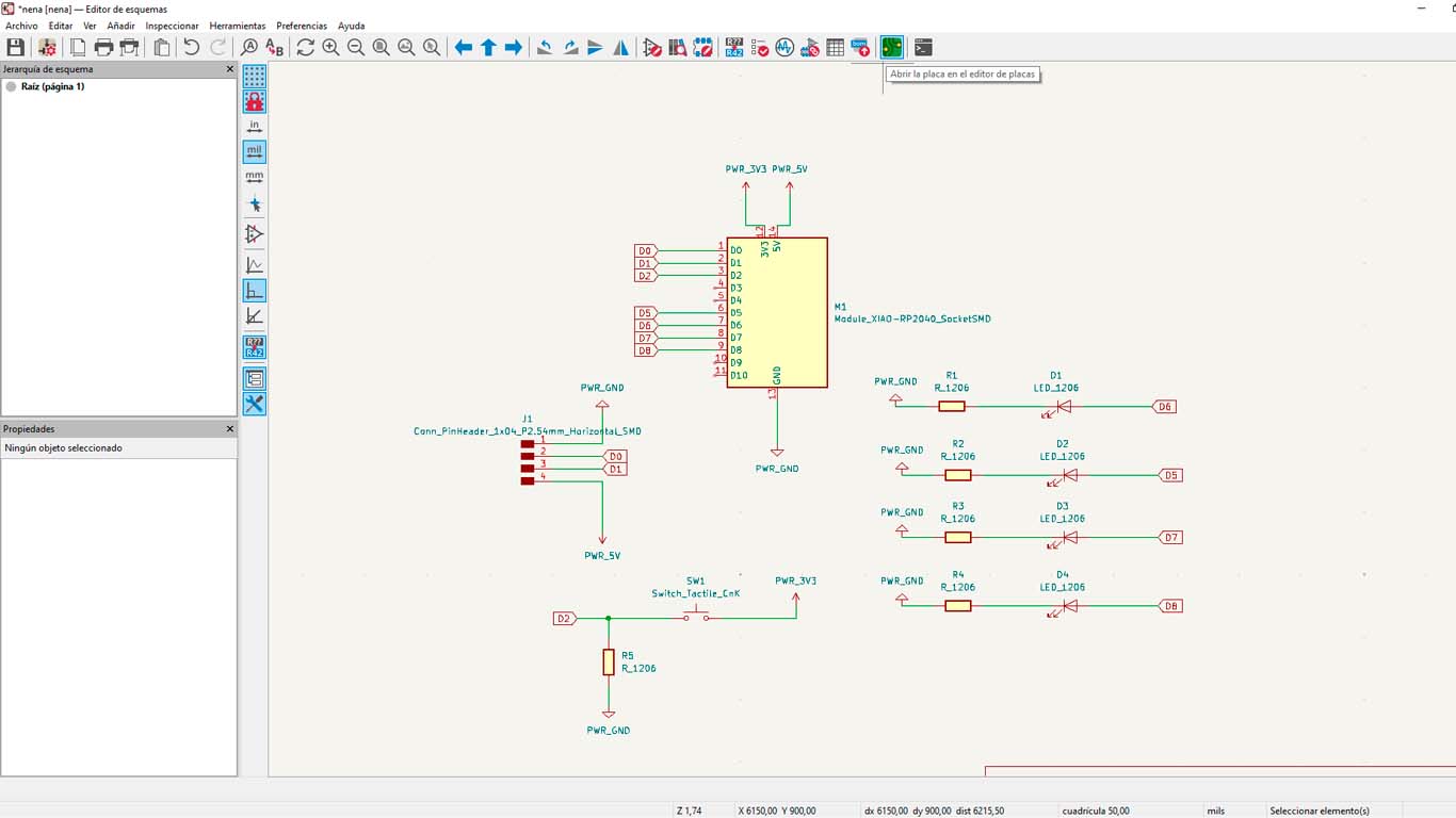
I will use the XIAO RP2040 also for this board since I will need more than 4 pins to develop the objective of the board. Likewise, we put all the components that the XIAO needs and choose the PINS that we are going to use.
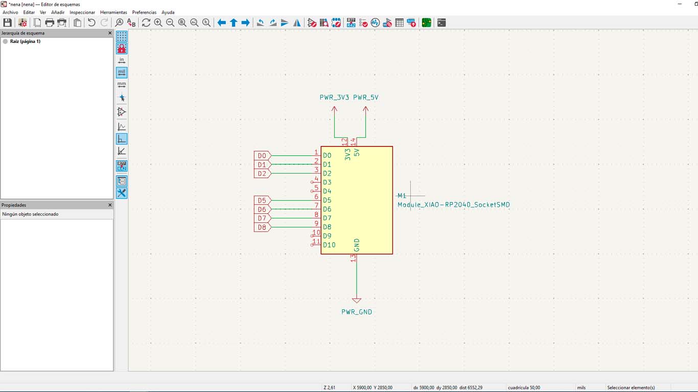
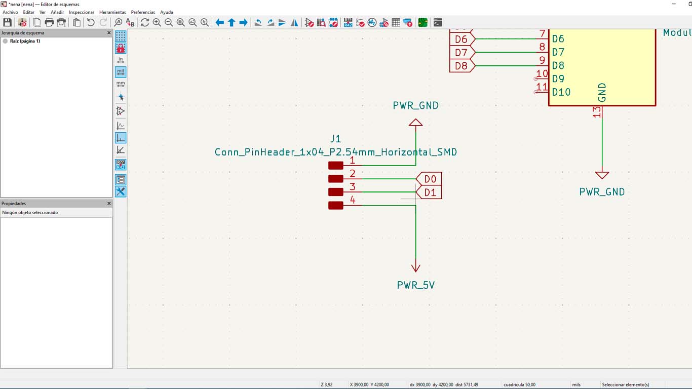
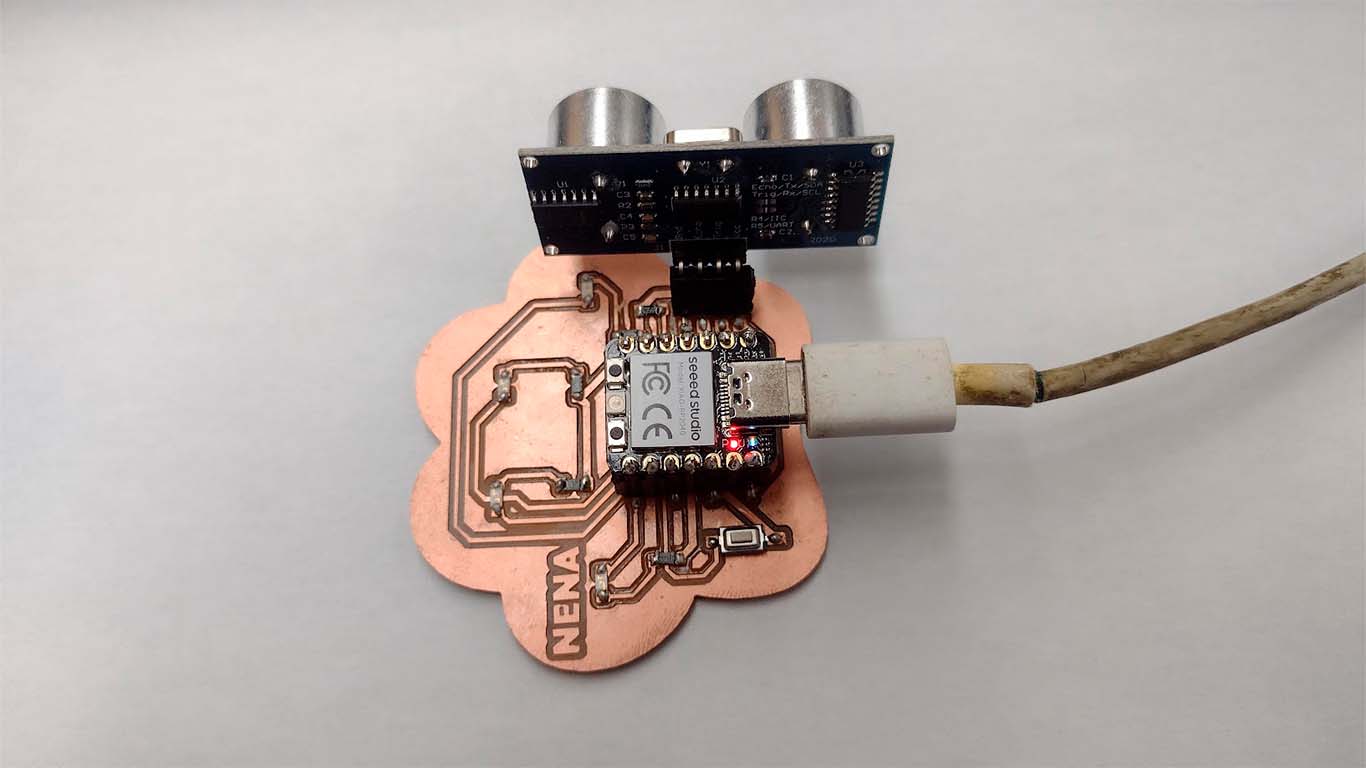
Then we will put a 4-pin female connector to place the ULTRASOUND that we will need to be able to measure the distance of the nearby object and it will also serve to turn on the LEDs each depending on the distance.
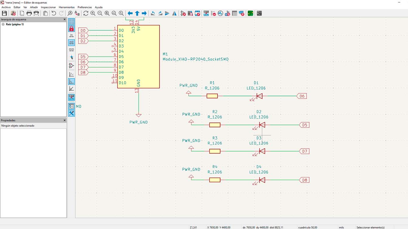
Likewise, we will add 4 LEDs to achieve the objective of the board and these will be connected to different PINS of the XIA RP2040
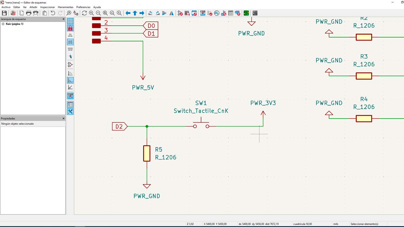
Finally, I will also place a switch so that when we push it, the LEDs will play with lights and we will be able to understand how our pet feels when playing with them.
Before exporting to the board design, let's always check that everything is fine, the connections are correct and move on to the design.
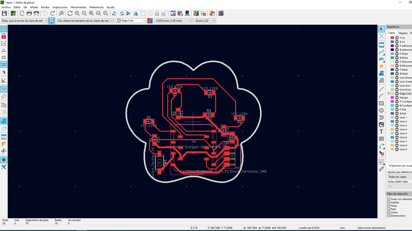
In the board design stage, you can place the components very close so as not to have traces that are too far away and close to other components that can affect each other.
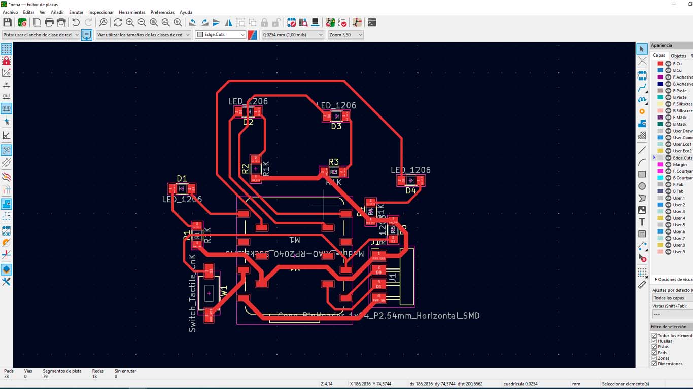
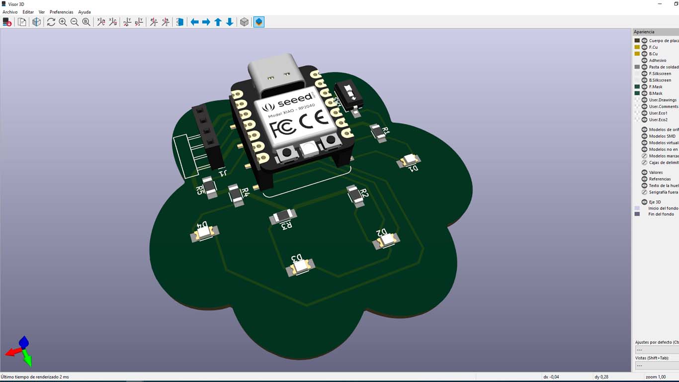
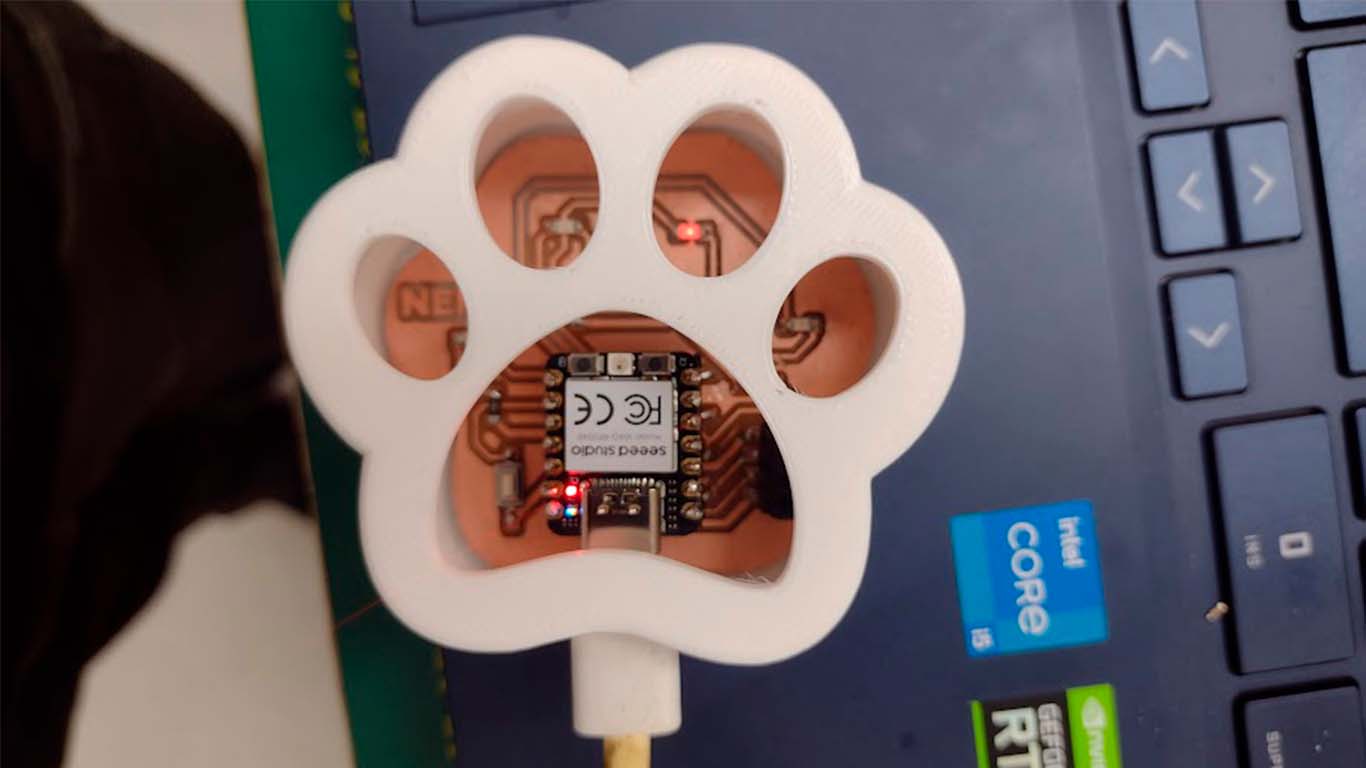
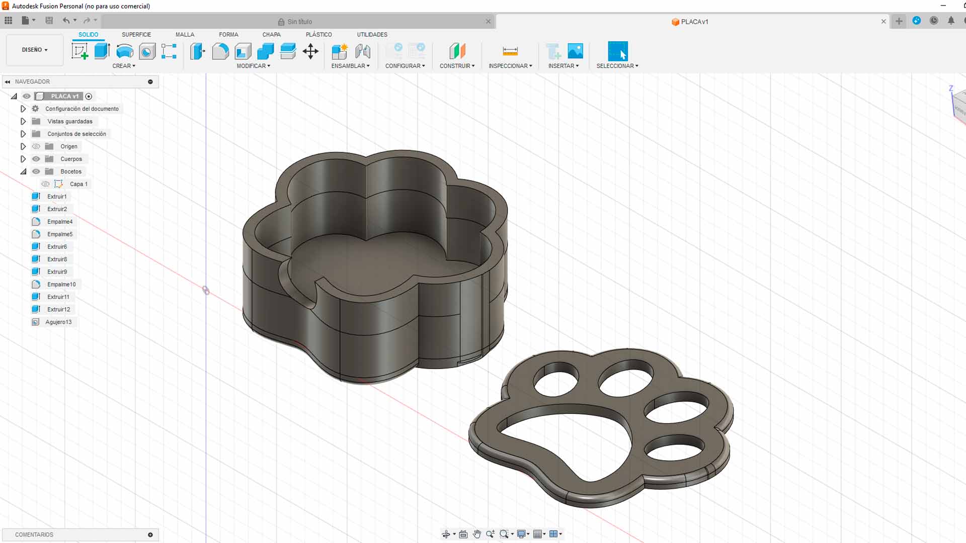
I had problems with what shape to give the board, in the end I decided on a dog's paw, the truth is that I liked how it looks, I arranged the components and the LEDs so that it can look very interesting and here are some screenshots of the board in 2D and 3D.
MAKING NENA BOARD
EXPORT TO MODS CE
After having the design, we export both the traces and the shape of our plate in SVG format and send it to MODS.CE, remember that the machine I used is the ROLAND SRM 20 and we must carry out all the steps for the machine to achieve the plate design. Here are some screenshots of the configuration for MODS.CE for both the traces and the border.
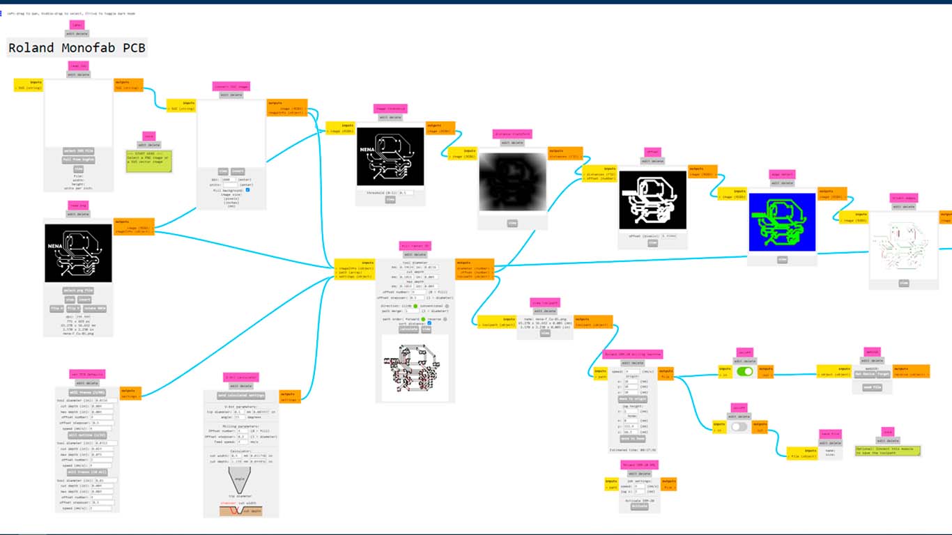
Let's remember to change the thickness of the cutter to 1/32, which is for cutting the board and is the one used for the perimeter of our board design.
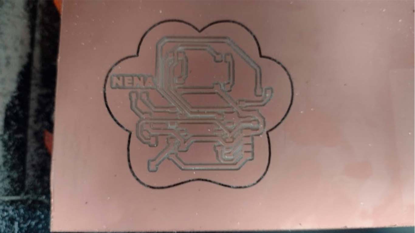
MILLING NENA BOARD
After configuring and reviewing our files in MODS CE we will move on to milling our board, first I started with the traces and then with the perimeter of the board. Here the process and the result of each of them.
COMPONENTS
Here is a list of the components that I am going to use on my development board.
| RESISTANCE: | 1K and 499 Ω |
|---|---|
| LED: | LED SMD RED |
| SWITCH: | SWITCH TACTILE |
| CONNECTOR: | 2 FEMALE CONNECTOR OF 7 AND 1 CONNECTOR OF 4 PINS |
| MICROCONTROLLER: | XIAO RP2040 |
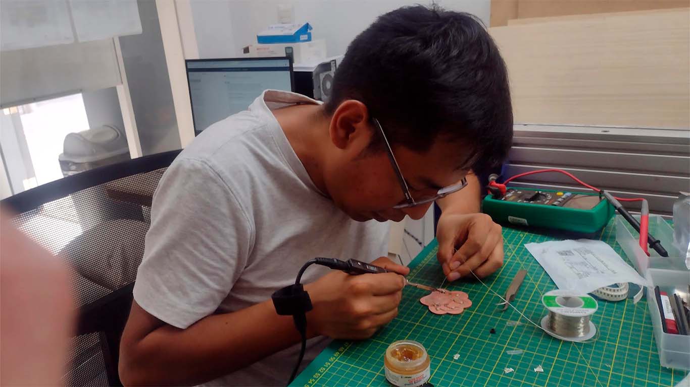
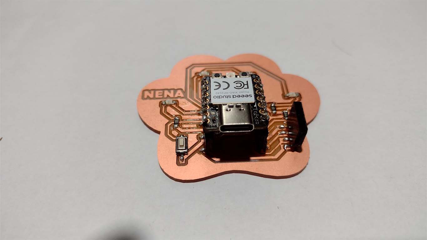
SOLDERING NENA BOARD
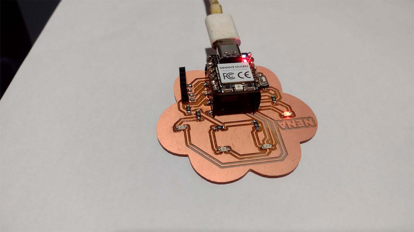
In the soldering process, I first started with the smaller components such as LEDs and Resistors. Then proceed to solder the female connectors for both the XIAO and the ultrasound component.
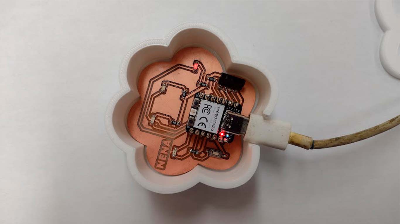
And finally, after soldering all the components, here is a photograph of how NENA BOARD is looking to start programming the LEDs. Don't forget to always check the continuity of the components and check the welding on each component.
WHAT DOES NENA BOARD DO?
TURN ON LEDs
First we will start checking if the LEDs all work. So I started programming them all together and keeping them on. Let's remember that first we have to configure our ARDUINO IDE to have the XIAO RP2040 release. Here I recommend you go to WEEK 4 so that you can configure before programming.
                                // Define the pins for the LEDs
                                    const int pinLED1 = 0;
                                    const int pinLED2 = 1;
                                    const int pinLED3 = 2;
                                    const int pinLED4 = 7;

                                    void setup() {
                                    // Configure the pins of the LEDs as output
                                    pinMode(pinLED1, OUTPUT);
                                    pinMode(pinLED2, OUTPUT);
                                    pinMode(pinLED3, OUTPUT);
                                    pinMode(pinLED4, OUTPUT);
                                    }

                                    void loop() {
                                    // Turn on the LEDs one by one
                                    digitalWrite(pinLED1, HIGH);
                                    delay(500); // Wait for half a second
                                    digitalWrite(pinLED2, HIGH);
                                    delay(500); // Wait for half a second
                                    digitalWrite(pinLED3, HIGH);
                                    delay(500); // Wait for half a second
                                    digitalWrite(pinLED4, HIGH);
                                    delay(500); // Wait for half a second

                                    // Turn off the LEDs one by one
                                    digitalWrite(pinLED1, LOW);
                                    delay(500); // Wait for half a second
                                    digitalWrite(pinLED2, LOW);
                                    delay(500); // Wait for half a second
                                    digitalWrite(pinLED3, LOW);
                                    delay(500); // Wait for half a second
                                    digitalWrite(pinLED4, LOW);
                                    delay(500); // Wait for half a second
                                    }
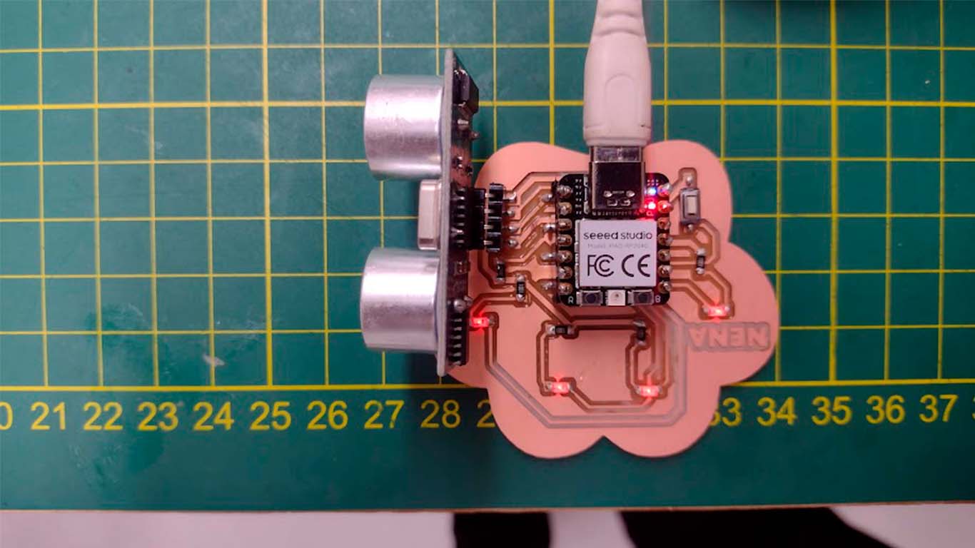
You can see that all the LEDs light up correctly, showing us that the welding and traces are correct. Now let's move on to another test.
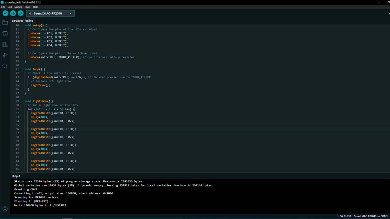
SWITCH FOR LEDS
To test with the SWITCH we will make the LED lights turn on and have a set of lights after pressing the switch, this to test if it works. Here the result.
                                // Define the pins for the LEDs
                                const int pinLED1 = 0;
                                const int pinLED2 = 1;
                                const int pinLED3 = 2;
                                const int pinLED4 = 7;

                                // Define the pin for the switch
                                const int switchPin = 28;

                                void setup() {
                                  // Configure the pins of the LEDs as output
                                  pinMode(pinLED1, OUTPUT);
                                  pinMode(pinLED2, OUTPUT);
                                  pinMode(pinLED3, OUTPUT);
                                  pinMode(pinLED4, OUTPUT);

                                  // Configure the pin of the switch as input
                                  pinMode(switchPin, INPUT_PULLUP); // Use internal pull-up resistor
                                }

                                void loop() {
                                  // Check if the switch is pressed
                                  if (digitalRead(switchPin) == LOW) { // LOW when pressed due to INPUT_PULLUP
                                    // Perform LED light show
                                    lightShow();
                                  }
                                }

                                void lightShow() {
                                  // Run a light show on the LEDs
                                  for (int i = 0; i < 5; i++) {
                                    digitalWrite(pinLED1, HIGH);
                                    delay(100);
                                    digitalWrite(pinLED1, LOW);

                                    digitalWrite(pinLED2, HIGH);
                                    delay(100);
                                    digitalWrite(pinLED2, LOW);

                                    digitalWrite(pinLED3, HIGH);
                                    delay(100);
                                    digitalWrite(pinLED3, LOW);

                                    digitalWrite(pinLED4, HIGH);
                                    delay(100);
                                    digitalWrite(pinLED4, LOW);
                                  }
                                }
TEST WITH ULTRASOUND
To test the ultrasound programming I have tried to find the error, at first everything was fine, I checked each PIN, its connectivity, continuity and also with the support of CHAT GPT, but I cannot find what the problem is. At first I thought it was the XIAO, but I programmed the QUENTORRES, it was not the problem. The truth is I got frustrated because I couldn't get the ultrasound to work. But I hope to find the solution to the problem...
Here is a video of the programming and as always the ultrasound read 0 at a distance, I checked everywhere but I don't know what the problem could be. Maybe here I leave the programming code.
                                // Define ultrasonic sensor pins
                                    const int trigPin = 26;
                                    const int echoPin = 27;

                                    // Variables to store pulse duration and distance
                                    long duration;
                                    int distance;

                                    void setup() {
                                    // Set pins as input or output
                                    pinMode(trigPin, OUTPUT);
                                    pinMode(echoPin, INPUT);

                                    // Start serial communication to display results on the serial monitor
                                    Serial.begin(9600);
                                    }

                                    void loop() {
                                    // Clear trigger pin
                                    digitalWrite(trigPin, LOW);
                                    delayMicroseconds(2);

                                    // Send a pulse to trigger pin
                                    digitalWrite(trigPin, HIGH);
                                    delayMicroseconds(10);
                                    digitalWrite(trigPin, LOW);

                                    // Measure pulse duration received on echo pin
                                    duration = pulseIn(echoPin, HIGH);

                                    // Convert pulse duration to distance
                                    distance = duration * 0.034 / 2;

                                    // Display distance on serial monitor
                                    Serial.print("Distance: ");
                                    Serial.print(distance);
                                    Serial.println(" cm");

                                    // Wait a little before next measurement
                                    delay(1000);
                                    }
For test 2, I used cables to see how the ultrasound worked, I checked the continuity but it did not send me any data when programming, I really don't understand what could be failing.
NENA BOARD OPERATION
LIGHT SEQUENCE
The LED sequence was to be used when the board was not reading any data near the board. And the idea is that every time something approached the plate, everything would turn off and turn on little by little LED by LED until it was very close to the plate and the next light play mode would happen.
LIGHT SET WITH LEDS
The intention with this programming was that when an object or person is very close to the plate that was measured by the ultrasound, it would have a set of LED lights as shown in the video. Here we can see how it would have more or less worked.
Here are some photos of how everything was assembled and to find the solution to make the board work 100%, I will find out...
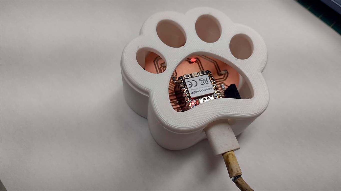
EXTRA CREDIT: DESIGN A CASE
DESIGN A CASE
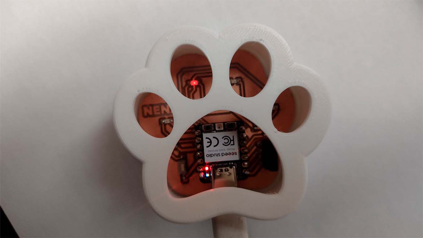
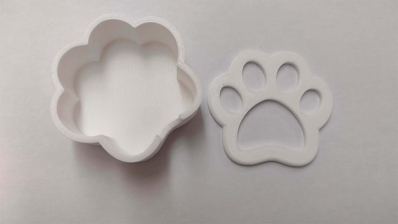
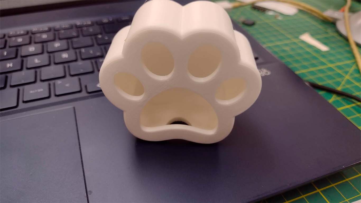
For the case I had thought about making a dog's leg with holes so that you can see the inside of it. Where the LEDs can shine and see how everything works inside. Here my design process.
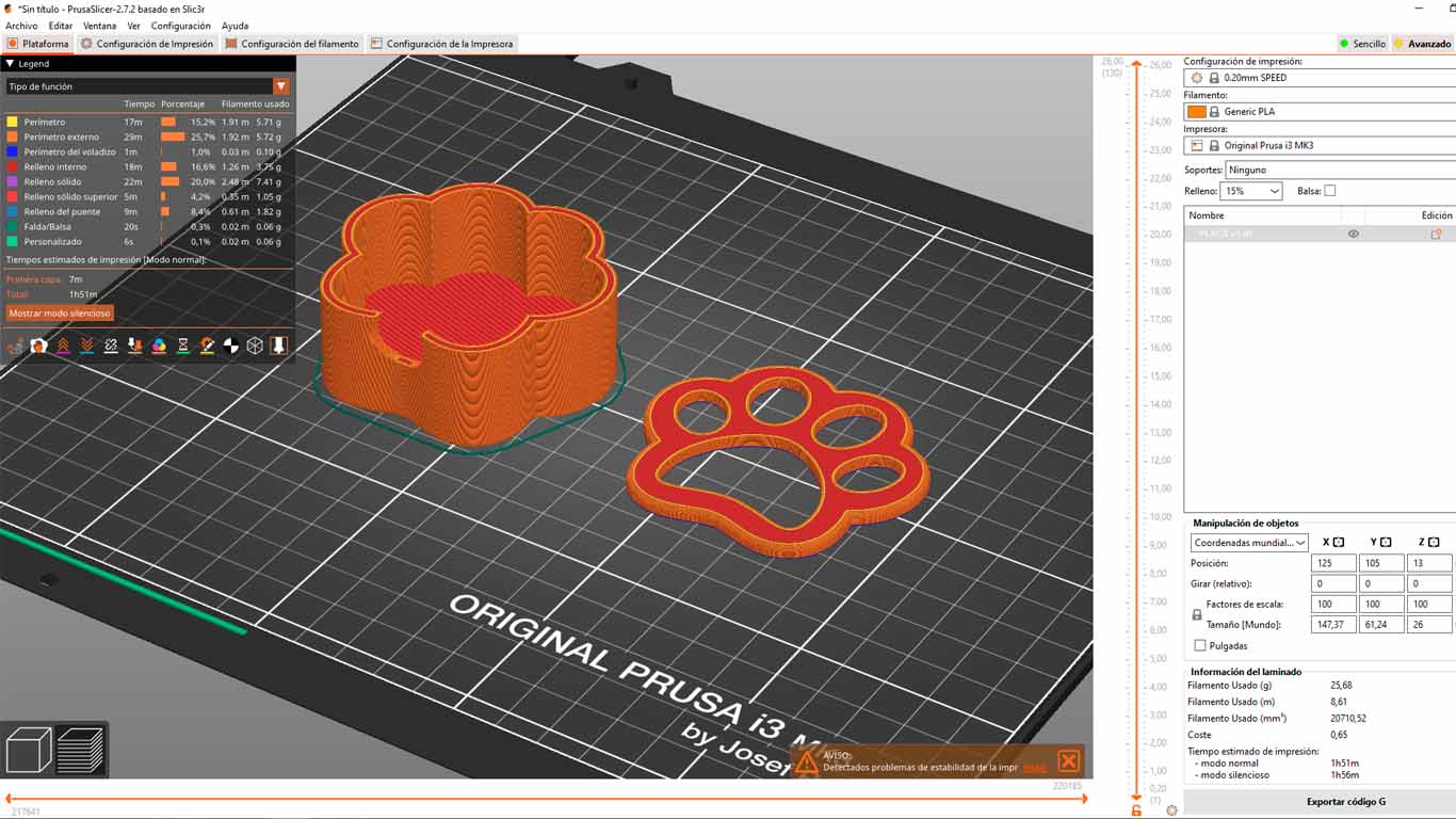
I used the FUSION program for the design since it seems very quick and easy to make the design, here is a view of the case.
After obtaining the design, I export it to the PRUSA SLICER program where I configure the 3D printing to obtain the case. On this occasion I will use PLA filament and here are some photographs and videos of the case process.
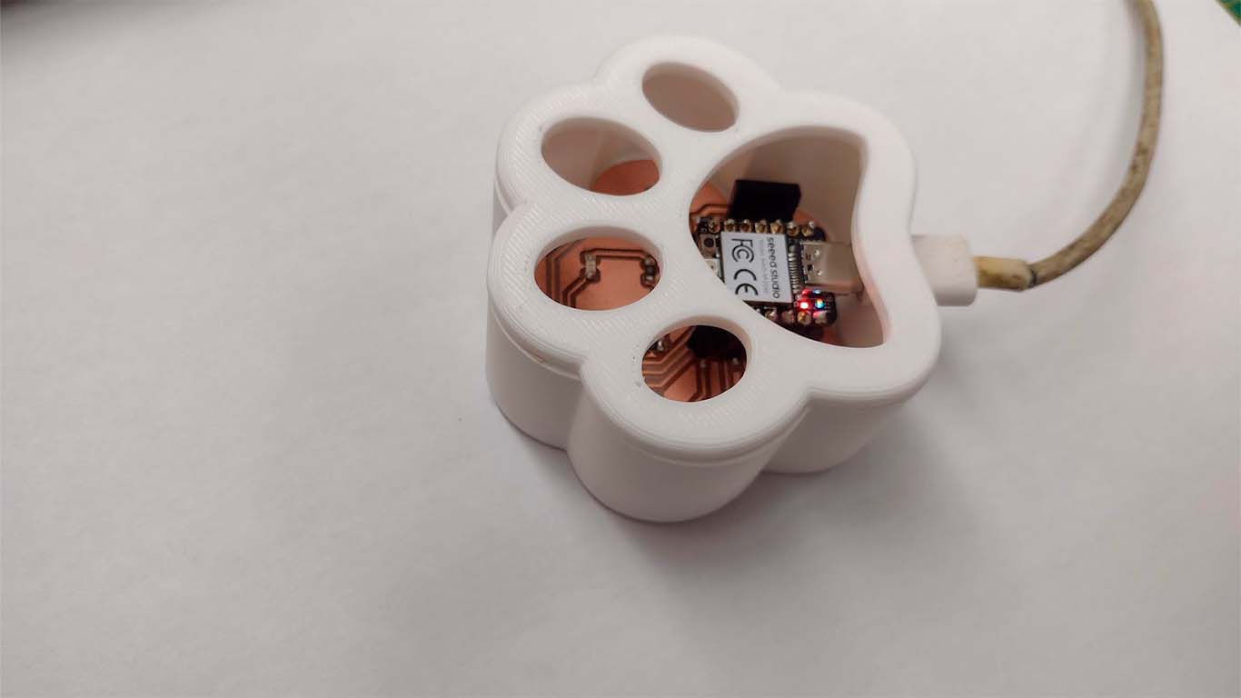
And here I managed to print with the PRUSA MK3 3D printer that we have at the FAB LAB UCSUR, with ABS filament and white color. I really like how it turned out and it was perfect for my board. Also thank my friend Maryori for supporting me in 3D printing.
Here are some photographs of how the plate looks inside the case.
FILES
Here you can download all the files that I have made for the following assignment: