This week's assignment was:
- Characterize the design rules for your in-house PCB production process
- Send a PCB out to a board house
- Make and test a microcontroller development board
- EXTRA CREDIT: personalize the board
- EXTRA CREDIT: make it with another process
ORGANIZATION
Here I show how I organized myself for this week.
| Wednesday 14th: | Fab Academy classes |
|---|---|
| Thursday 15th: | Review of all implements to carry out the group assignment and investigation of machine uses. |
| Friday 16th: | Preparation of group assignment test and first documentation of the week. |
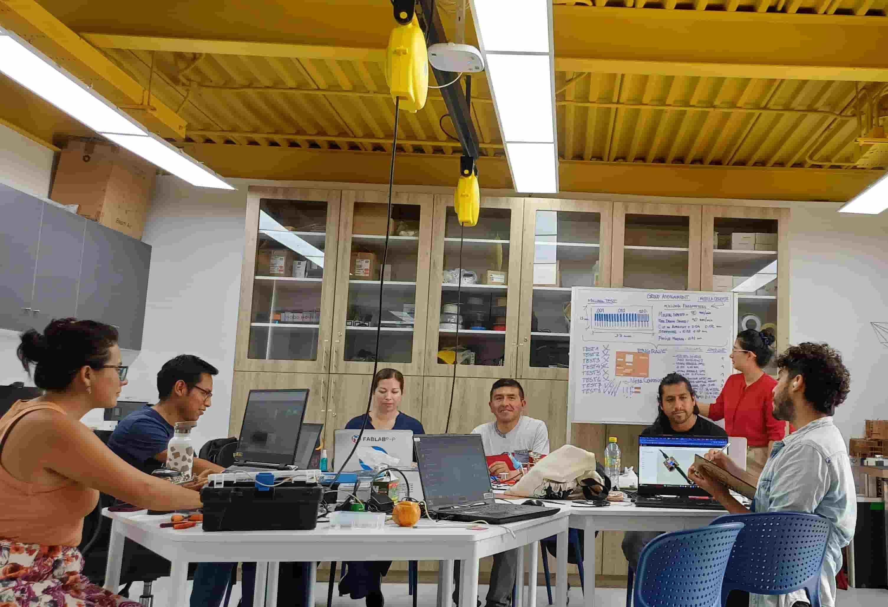
| Saturday 17th: | In-person meeting with the group to understand the group assignment and plate welding test. |
| Sunday: 18th: | Documentation and commit of the advanced. |
| Monday 19th: | Milling of my plate for individual order and development of QUENTORRES model design. |
| Tuesday 20th: | Soldering of components on board and final documentation. |
GROUP ASSIGNMENT
Here I leave the link to go to the group assignments page.
Clic here to visit the WEEK 4 GROUP ASSIGNMENT PAGE
PCB PRODUCTION PROCESS
INVENTORY
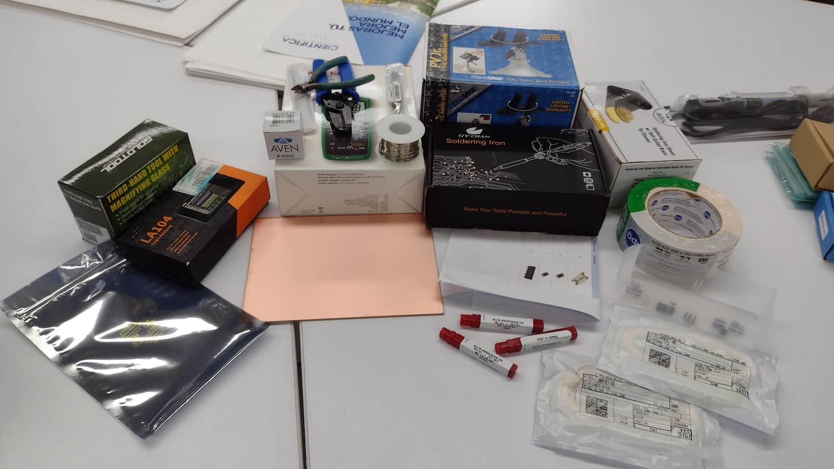
Before starting the assignments, my friend Maryori and me made a complete inventory of all the electrical components and tools we need for this week. Likewise, we also carry out an inventory to have everything in order and see what things we need to request it.
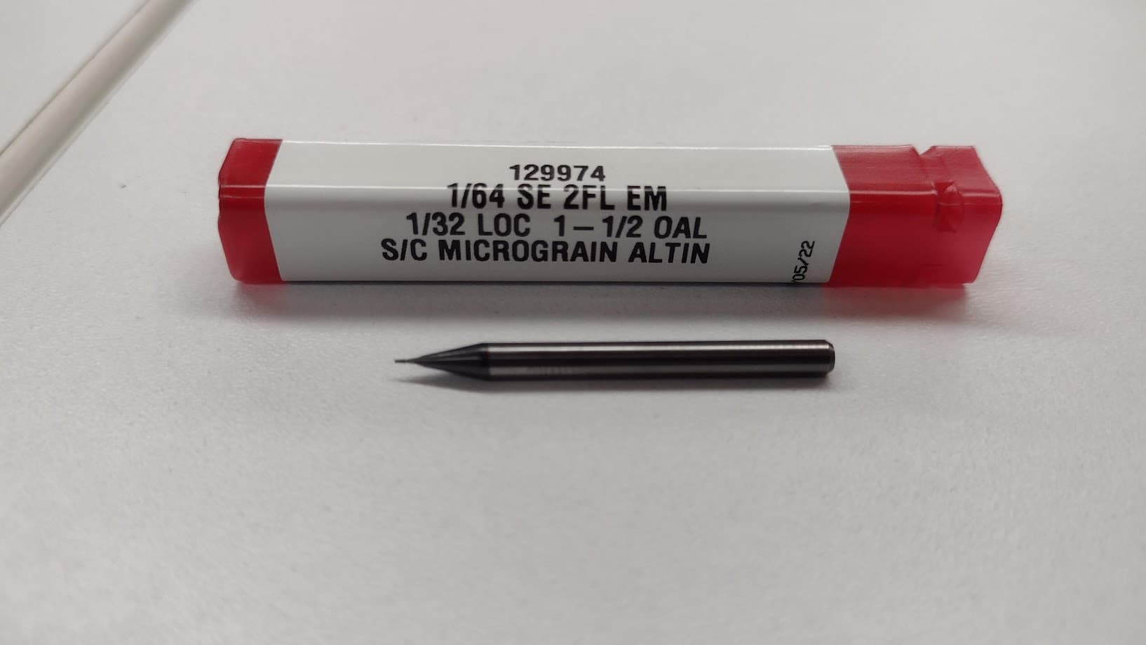
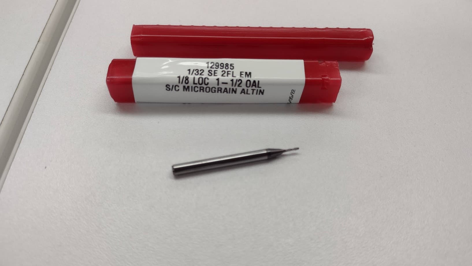
I could see that we have the 1/64 and 1/32 cutters that are going to be essential for this assignment. Here I leave a photograph of each of them.
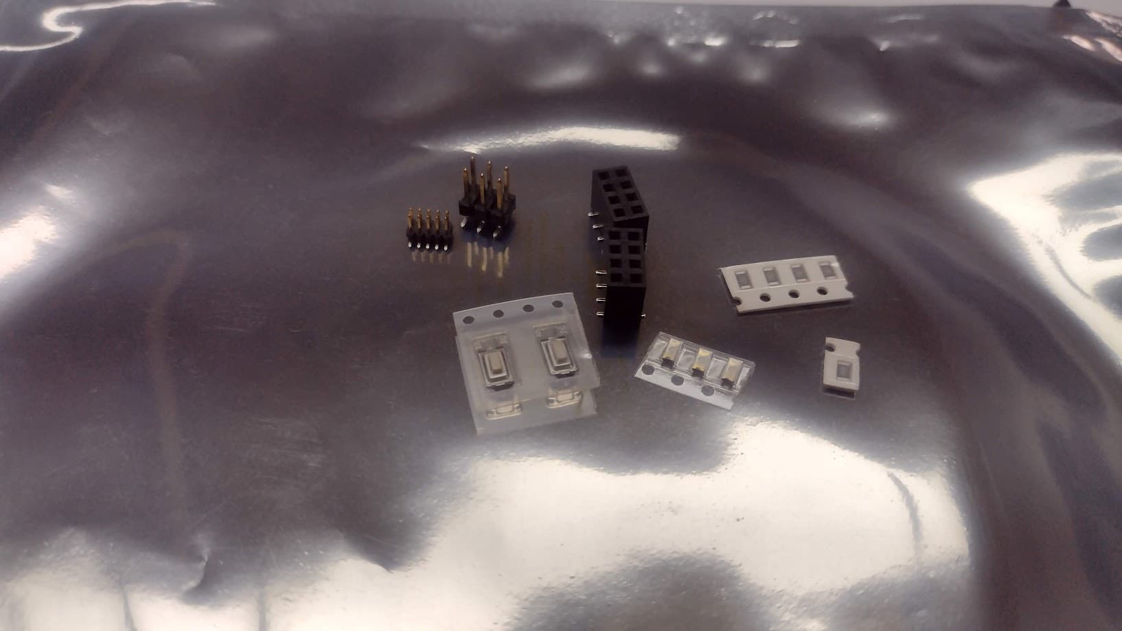
Finally, here is a photograph of the electronic components that we need to carry out the group and individual assignment.
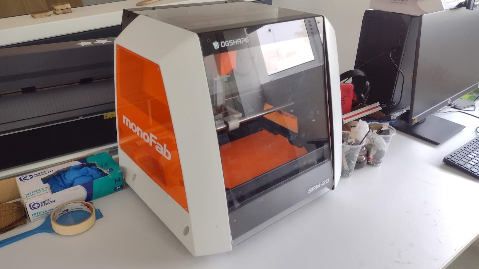
MILLING MACHINE
The milling machine that we have at the Universidad Cientifica del Sur is the MONOFAB SRM-20 that we will use for this week's assignment. Here are some specifications of the machine:
| WORK SURFACE | 232.2 x 156.6 mm |
|---|---|
| OPERATING SPEED | 6 mm/min to 1.800 mm/min |
| POWER CONSUMPTION | 50 w |
| SPINDLE ROTATION SPEED | 3.000 RPM to 7.000 RPM |
TRACE WIDTH TEST
STEP 1: PREPARATION FOR MILLING
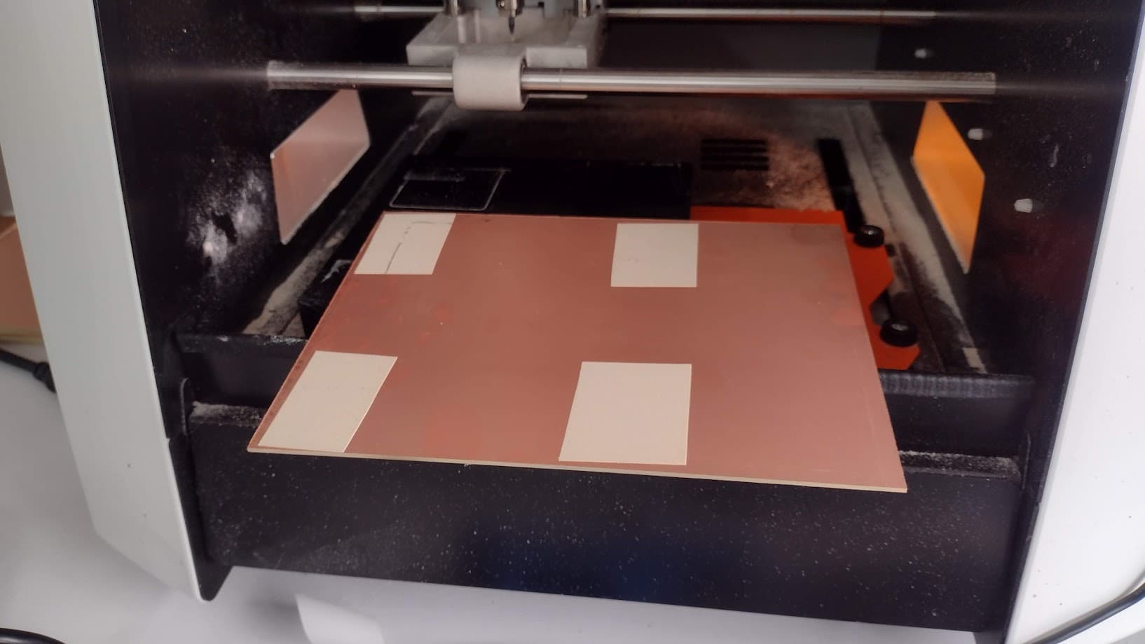
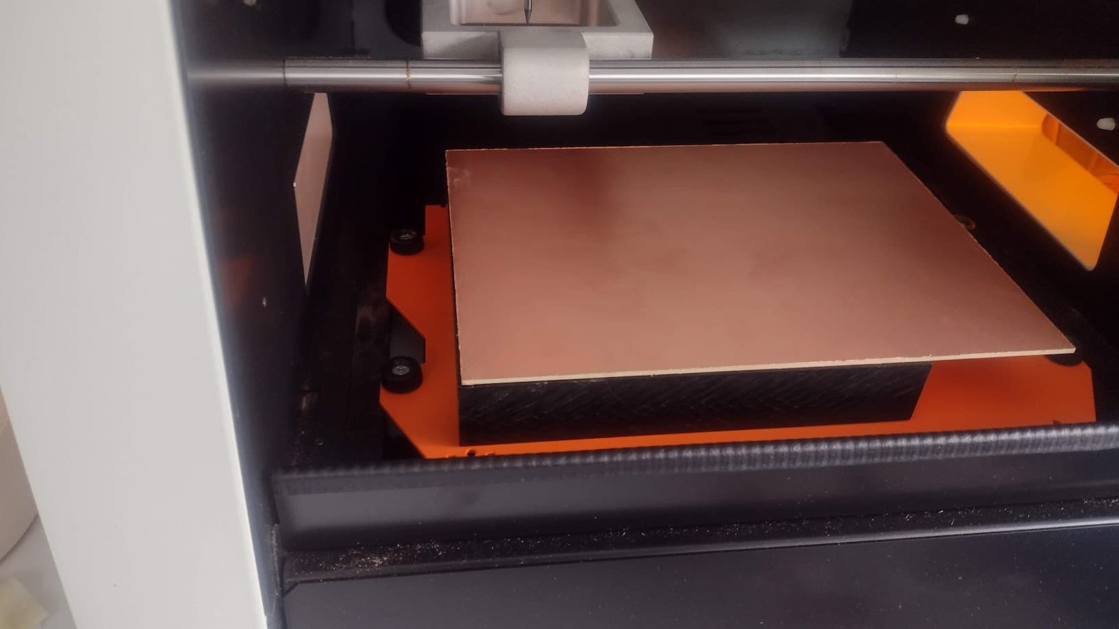
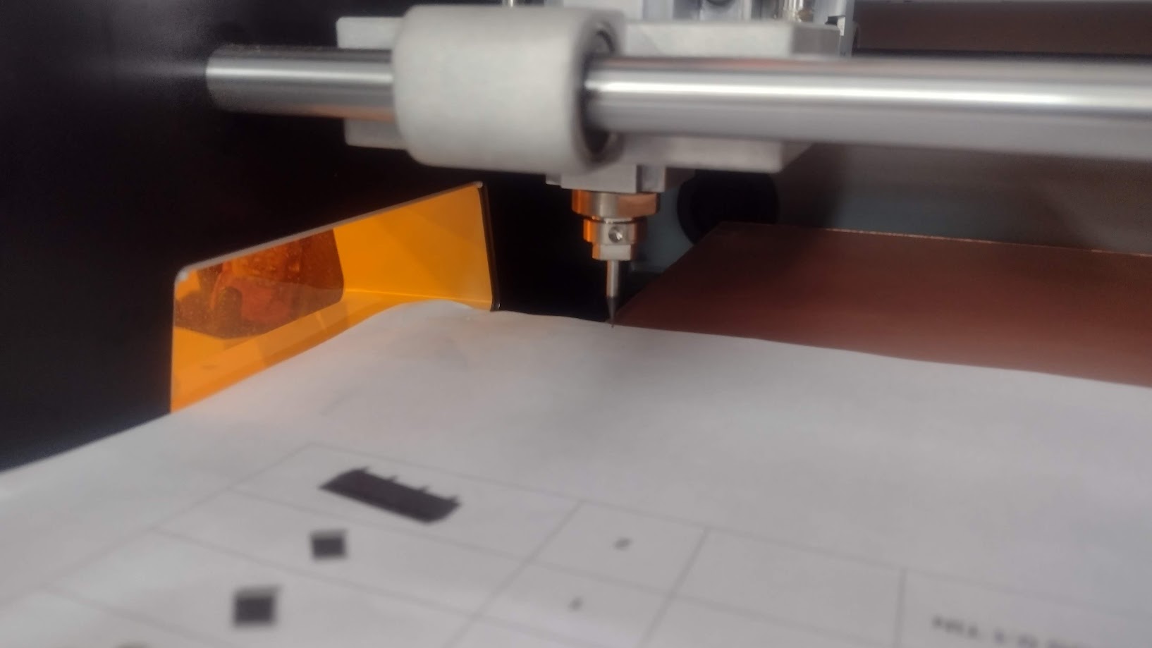
Before starting to cut the test we have to start with the preparation of the cutting area. Therefore, first we place the double contact tape on a small board so as not to work on the base of the machine, which is made of metal and can damage the cutters.
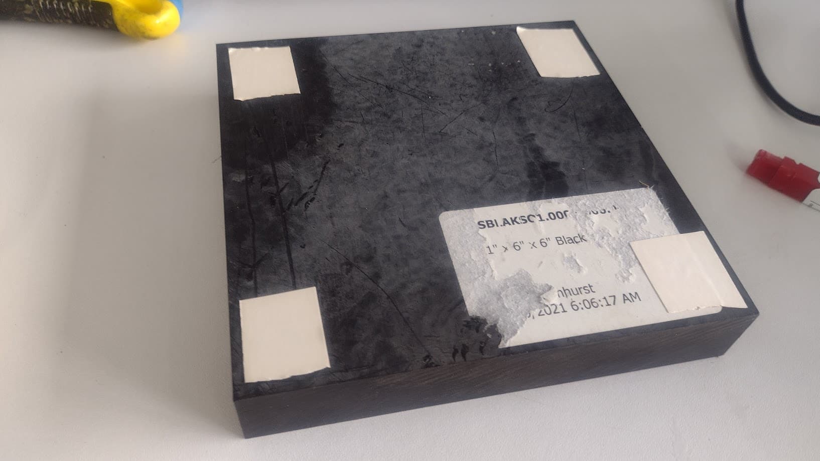
Then, we put more double contact tape on the board that we mentioned above so that we can stick the Printed Circuit Board so that they cannot move when the work is being done and we can take care of our milling cutter.
After having the circuit board correctly glued. We begin to configure the X, Y and Z axes of the MONOFAB . To do this, first we start configuring the X and Y axes where we want to start working and then, with the help of a bond sheet we can calculate the Z axis. Here we have to be careful because we can break the milling cutter if we don't do it right.
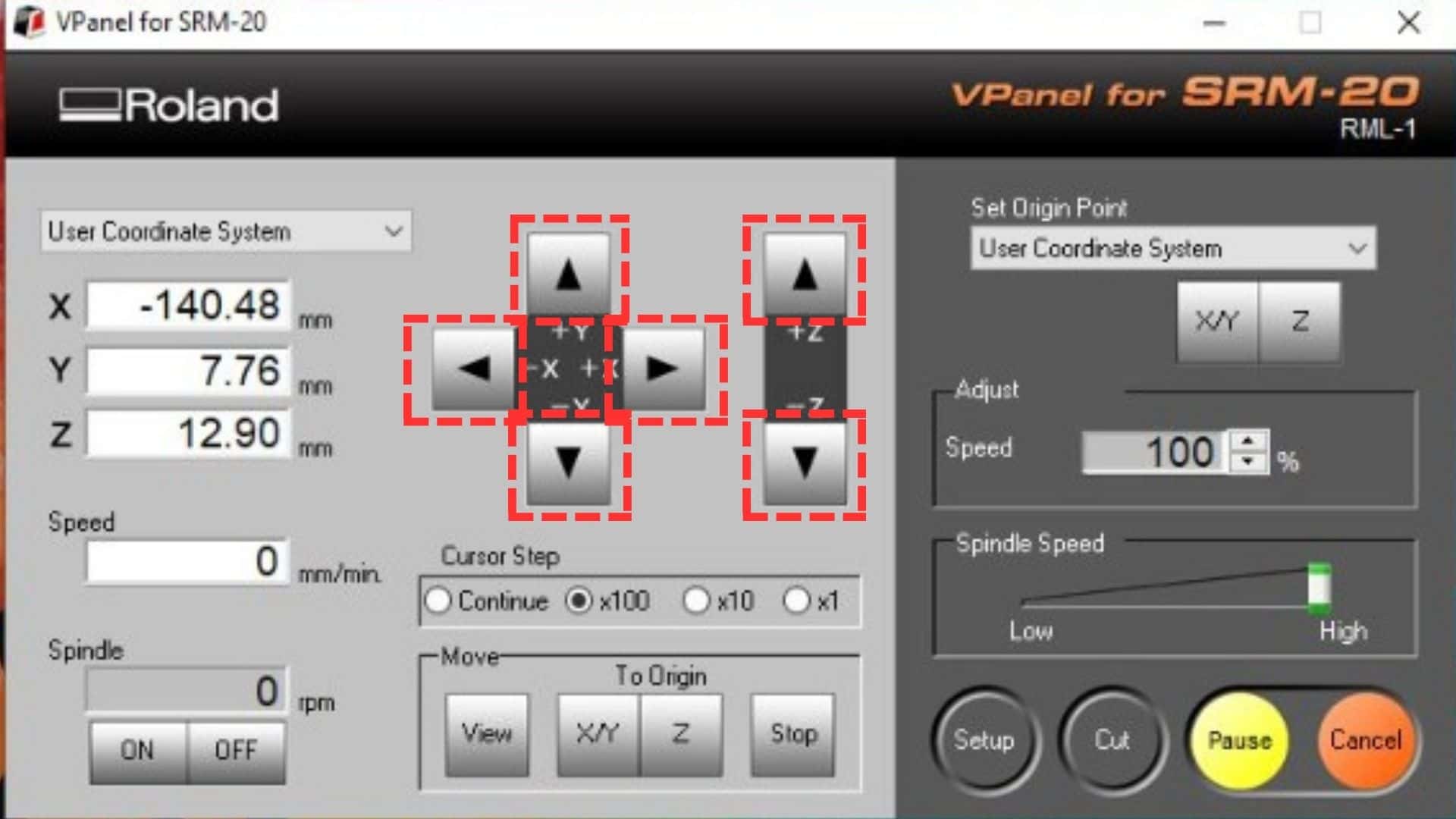
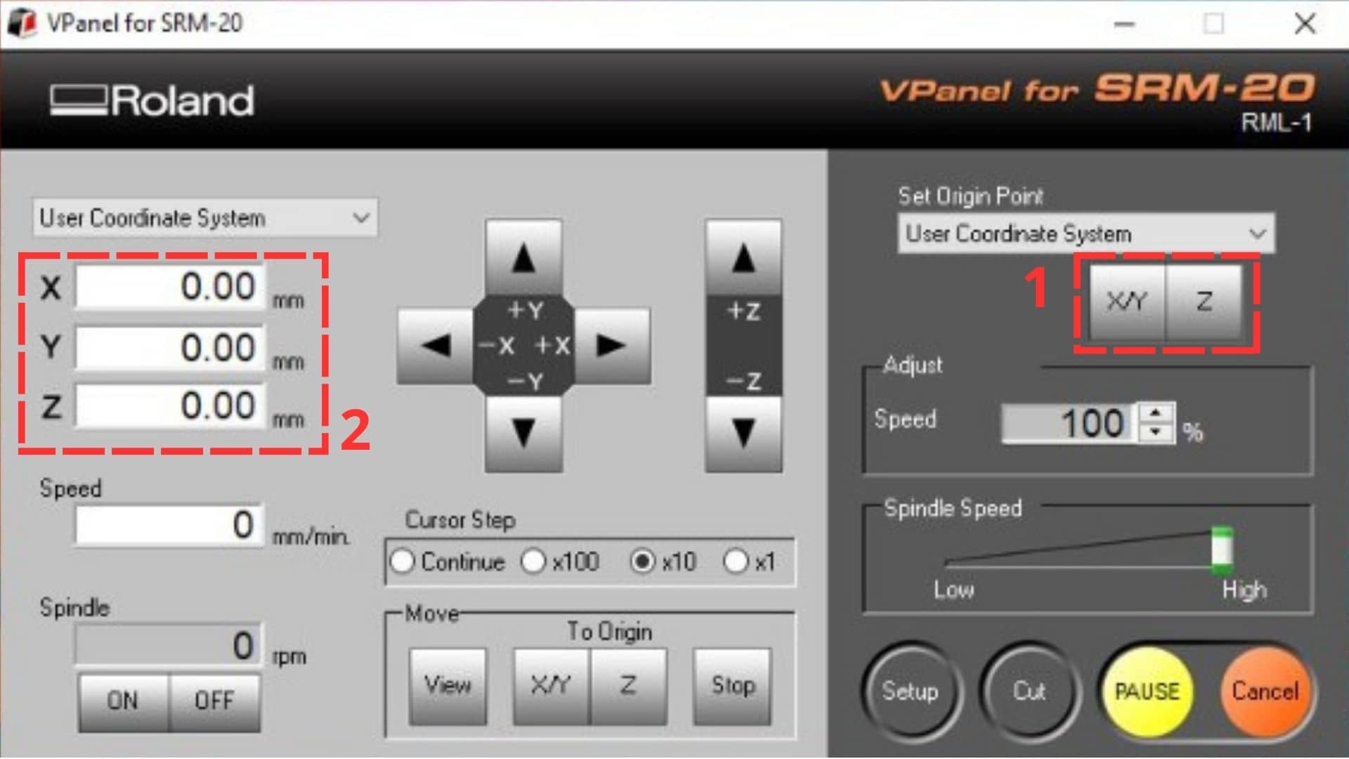
After obtaining the correct location of the X, Y and Z axes, we click SET ORIGIN since it will be the new origin of the machine and it can start cutting. That is where all the values will change to 0.00 mm and we would have the machine ready to start working.
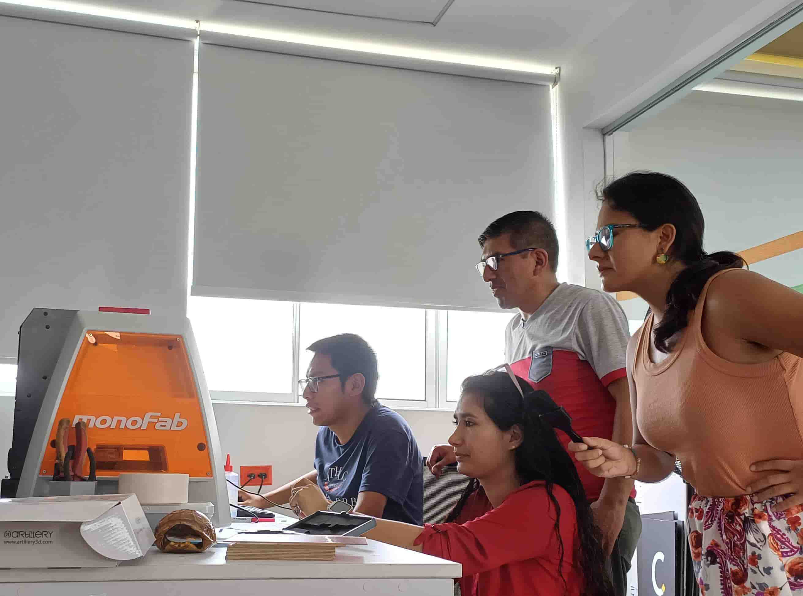
Here is a photo with my colleagues from FAB ACADEMY understanding and configuring the MONOFAB to continue with the assignments.
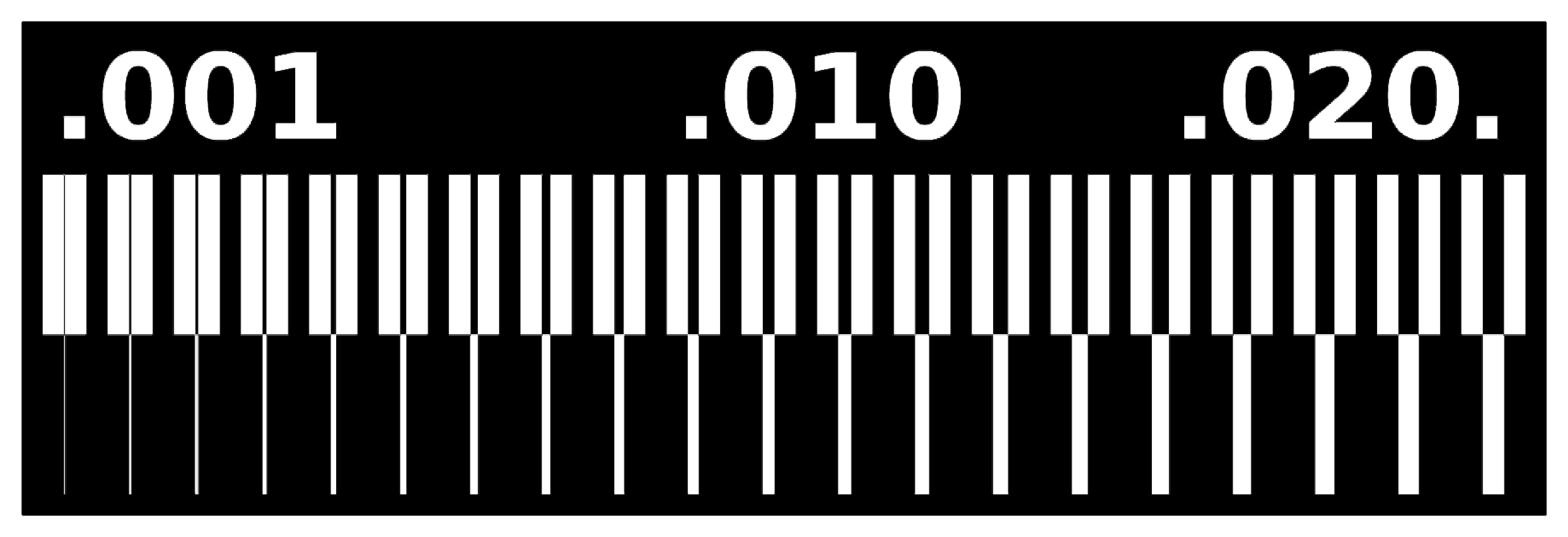
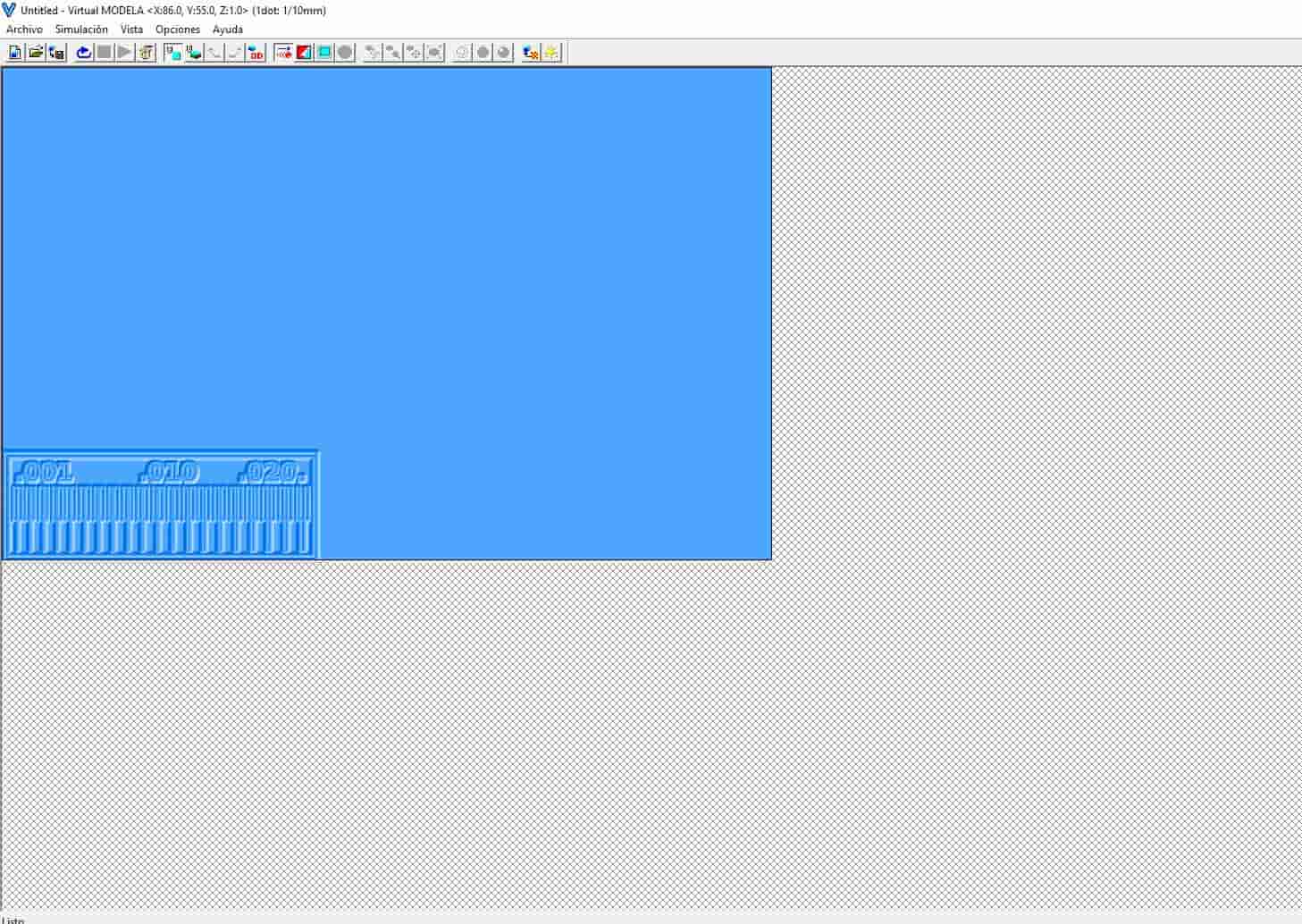
STEP 2: LINE TEST
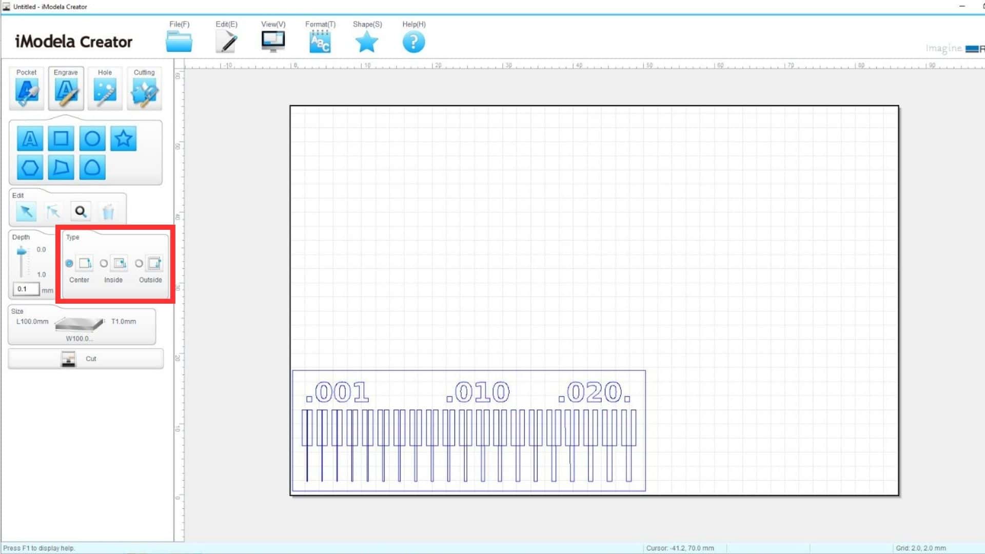
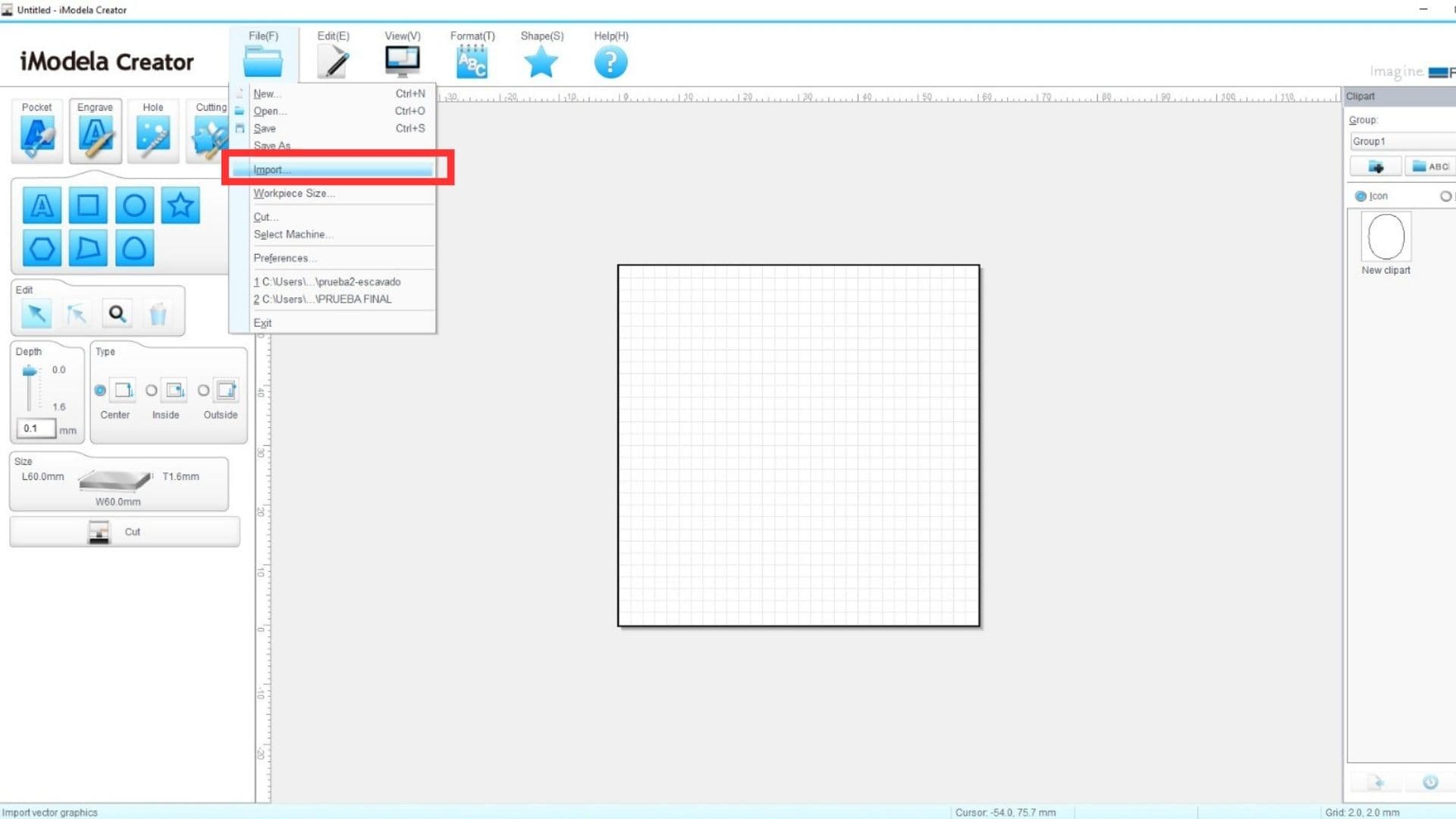
We will start with the line test, where we will perform the milling in the following image, remember that first we will perform the milling and then the cutting. For this first step we have to download the figure and pass it to the IMODELA CREATOR program , which is the program we use before moving to the machine program.
TRACES
INTERIOR

We first import the TRACES to IMODELA CREATOR to start milling and configuring the machine, remember that we will use the 1/64 drill bit for this occasion.
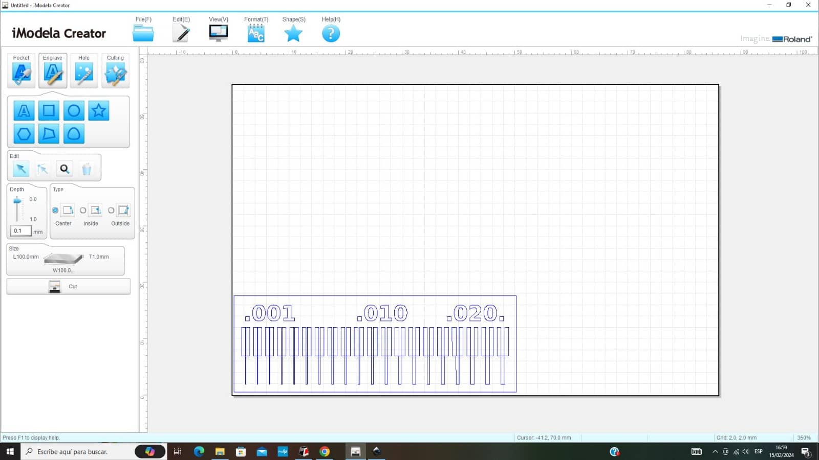
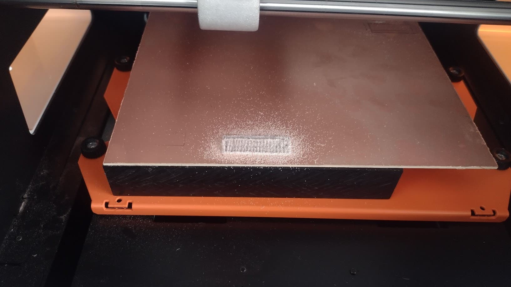
The IMODELA CREATOR program has the ability to show us a simulation of how the work we previously did would turn out. We thought it was good, so we sent it to be cut but the result was not what we expected.
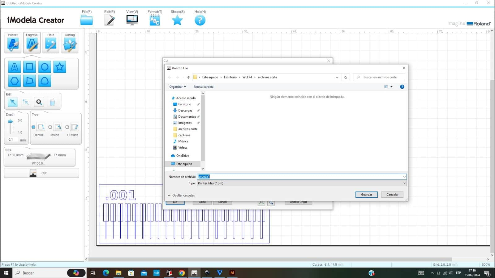
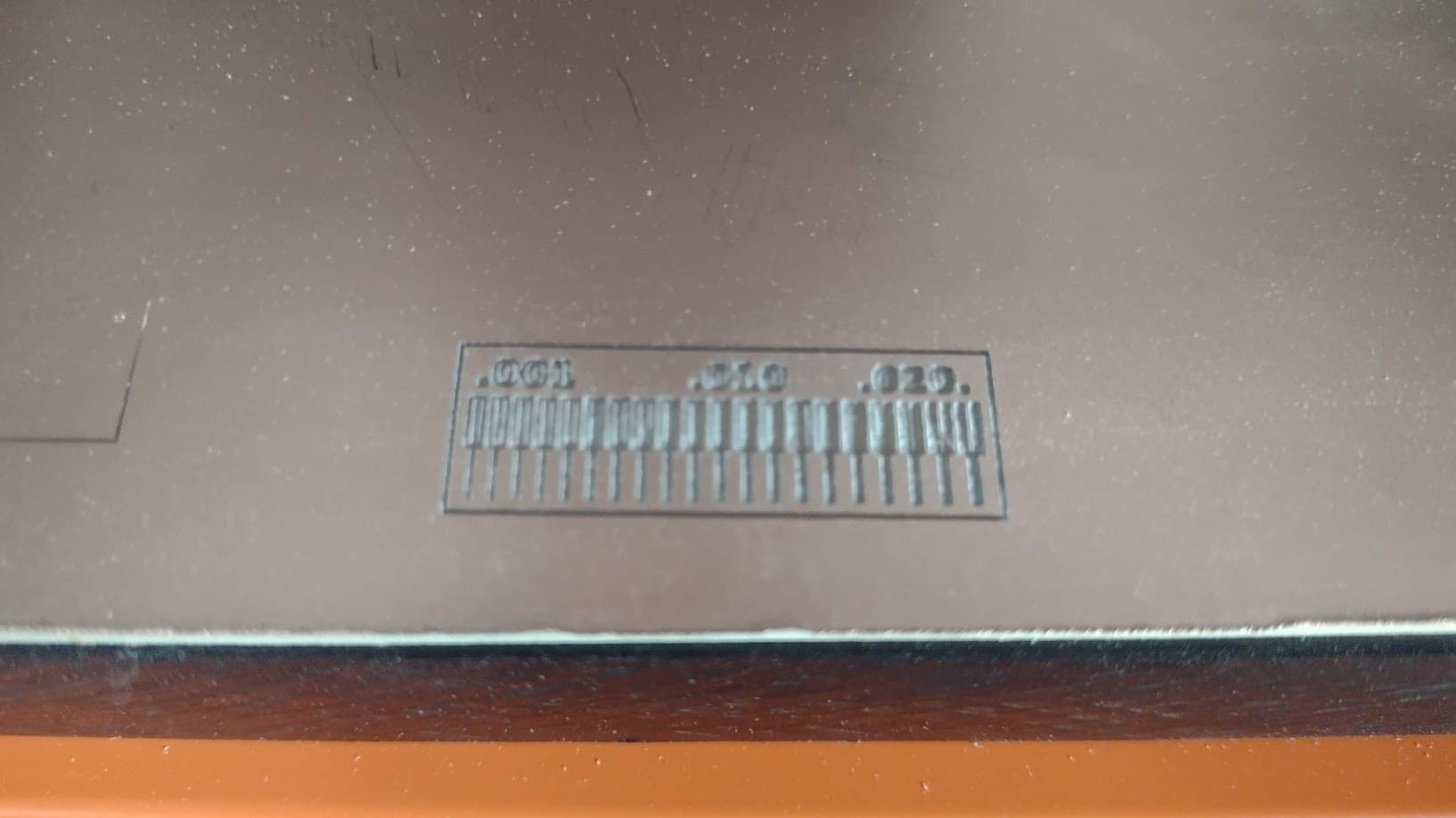
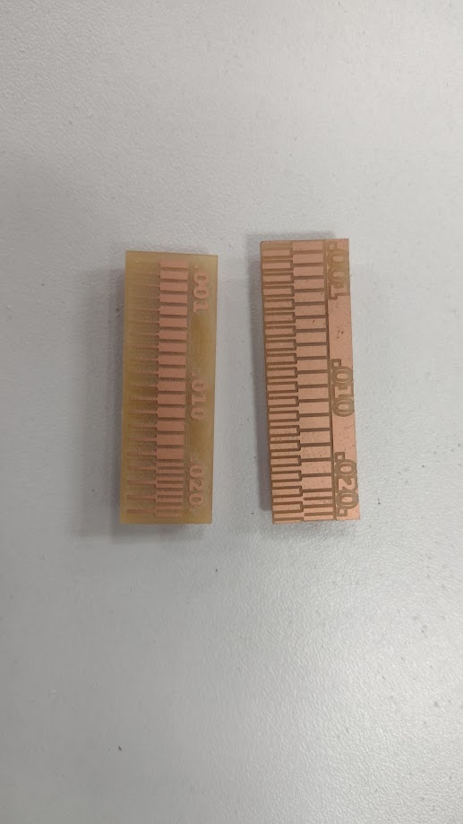
After importing, we proceed to cutting with the machine. In the first test we failed because the cut came out the other way around, that is, instead of cutting the part that we didn't need (black area), it started cutting the lines and numbers (white area) and this is the result. But the cut was precise and showed very well.
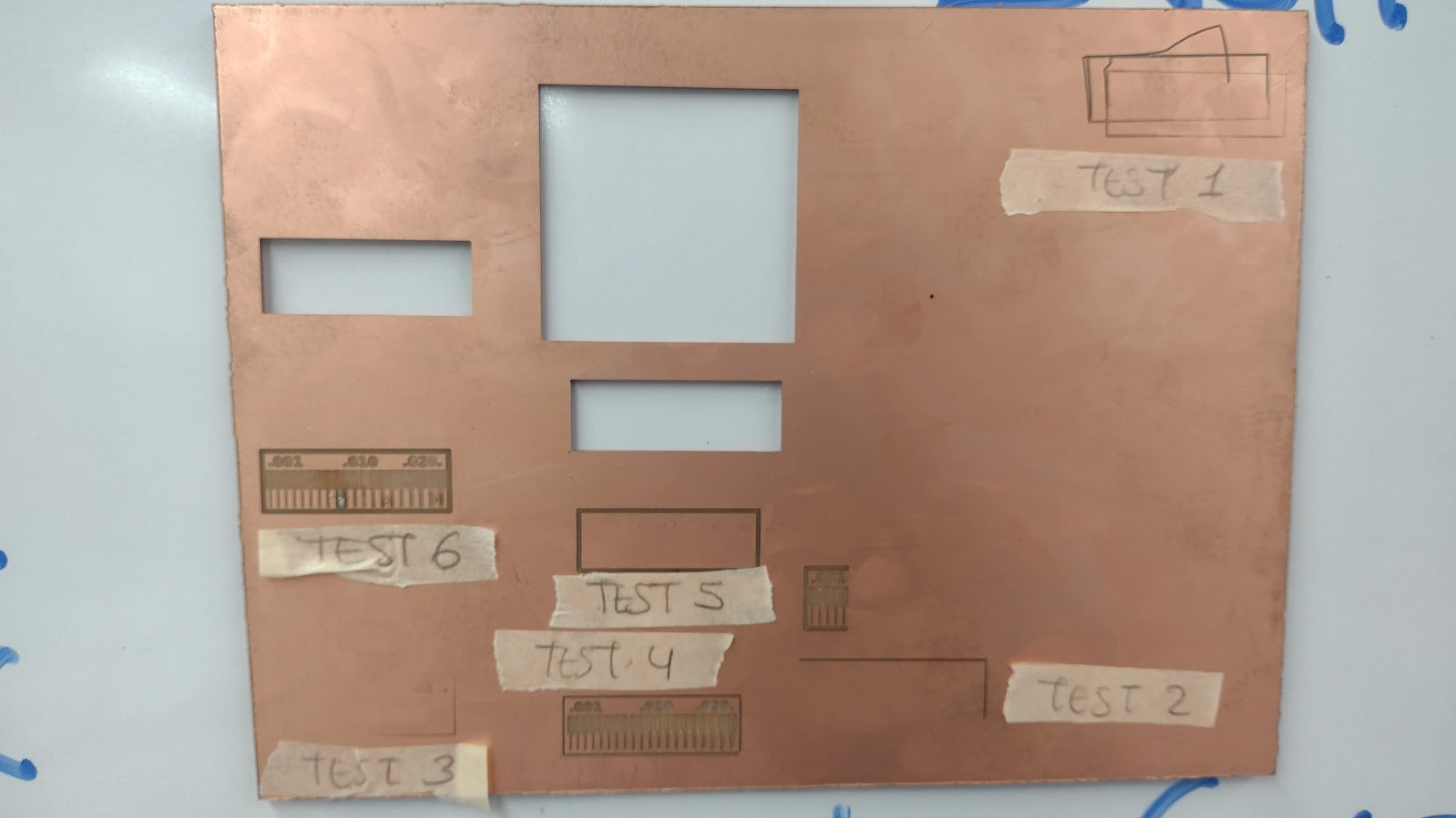
From here we had 5 more failures due to the frustration we had, we couldn't understand that we were wrong. Here is a photograph of the errors we had.
We talked with each other and agreed to review each procedure we are doing. We left the machine and began to discuss the failures and analyze each step we were taking. So we met, understood through whiteboard support and understood each failure.
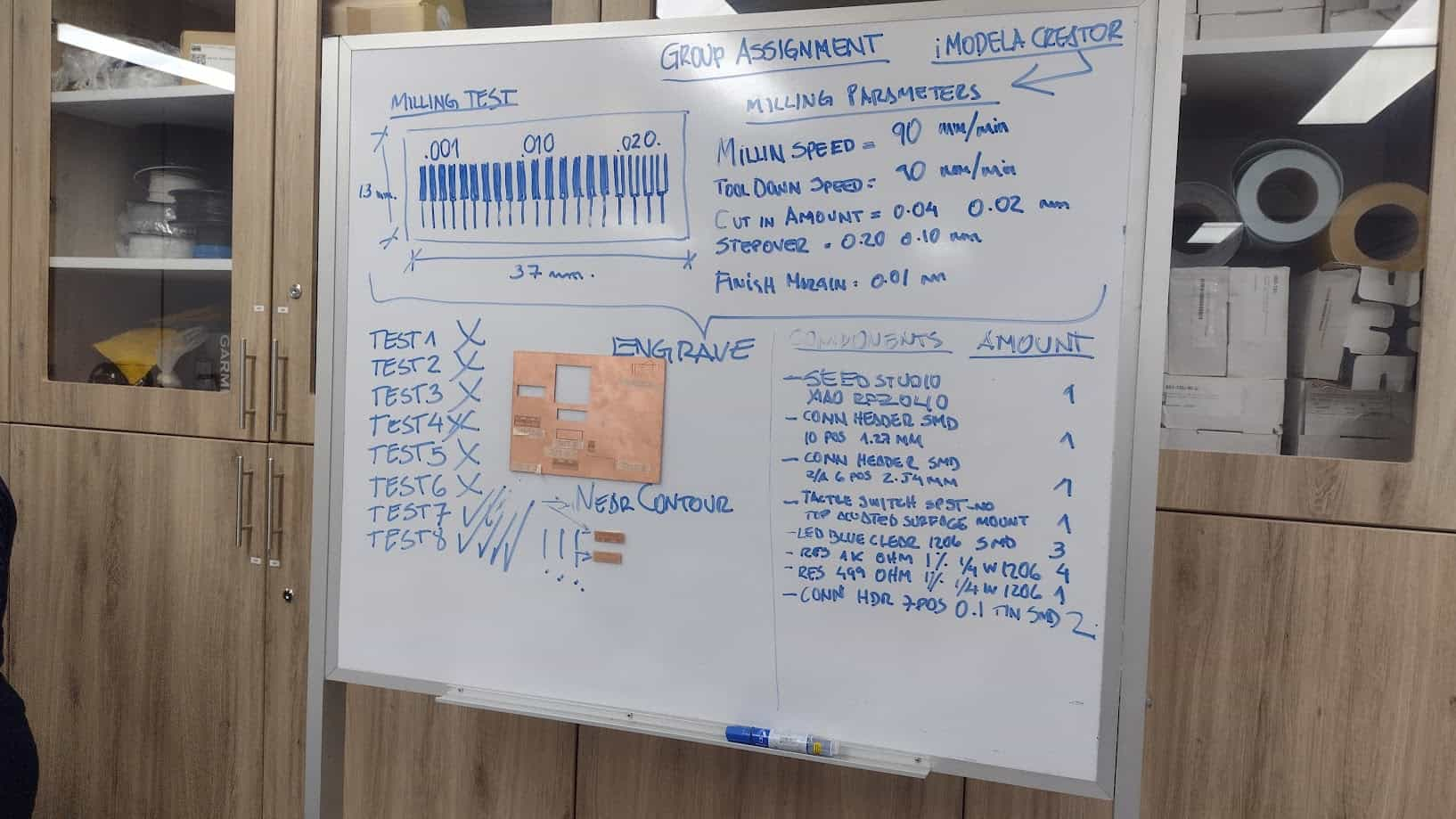
After taking a breath, we were able to understand and discover what the error was, but we were not able to achieve the objective. However, we were able to achieve what we were looking for when we sent the file to be milled and happily it turned out well and what we wanted for the machine to cut through the OFFSET. The problem was that we did not realize that in the software we could make changes so that the milling cutter cuts OUTSIDE, CENTER OR INSIDE and we configured it correctly and the test came out that was close to the objective.
Then, we also discovered the difference between POCKET, ENGRAVE, HOLE AND CUTTING that the software offers us. Then we made the corresponding configurations to make the test look like what other colleagues presented last year and we achieved it.
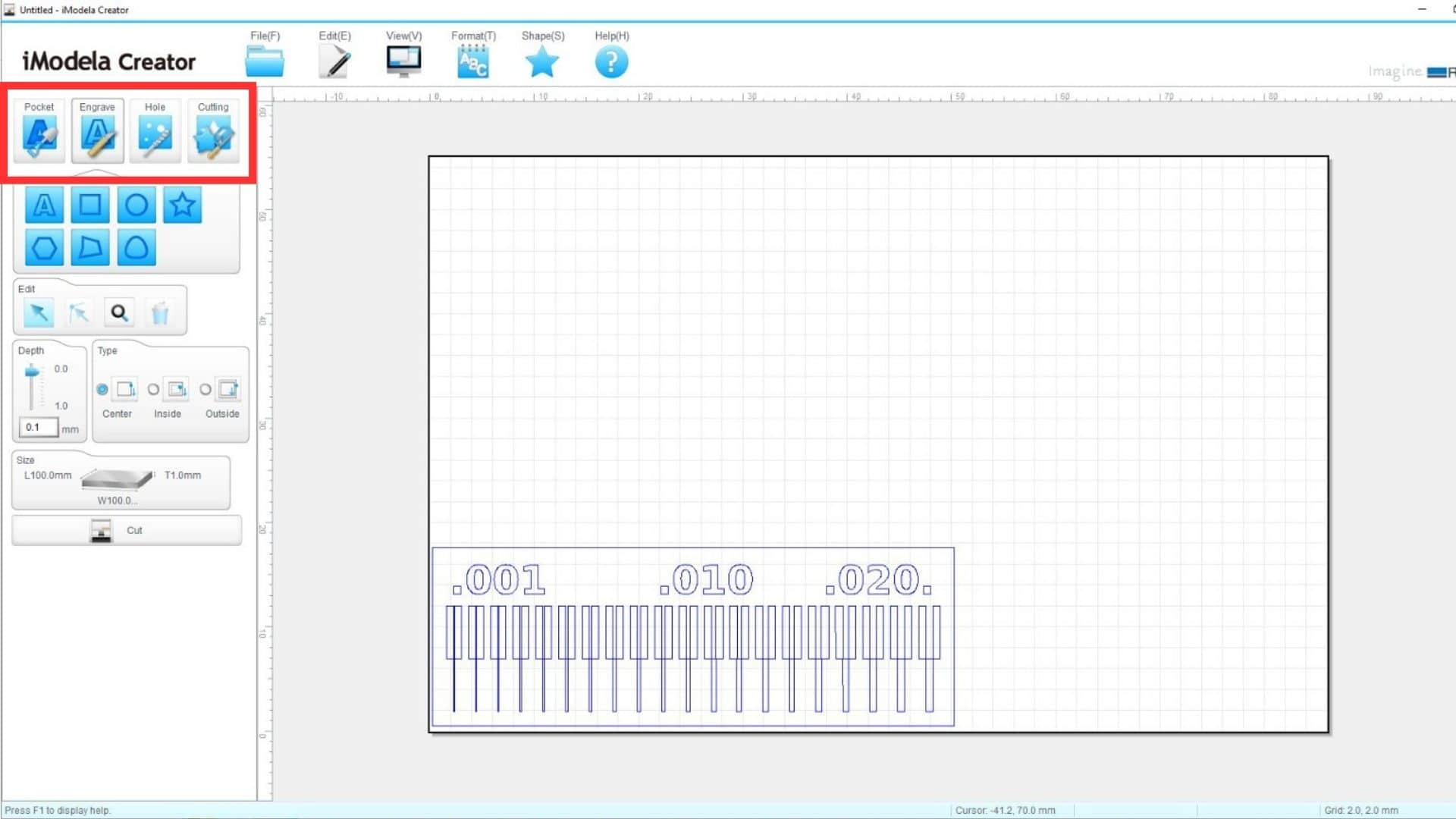
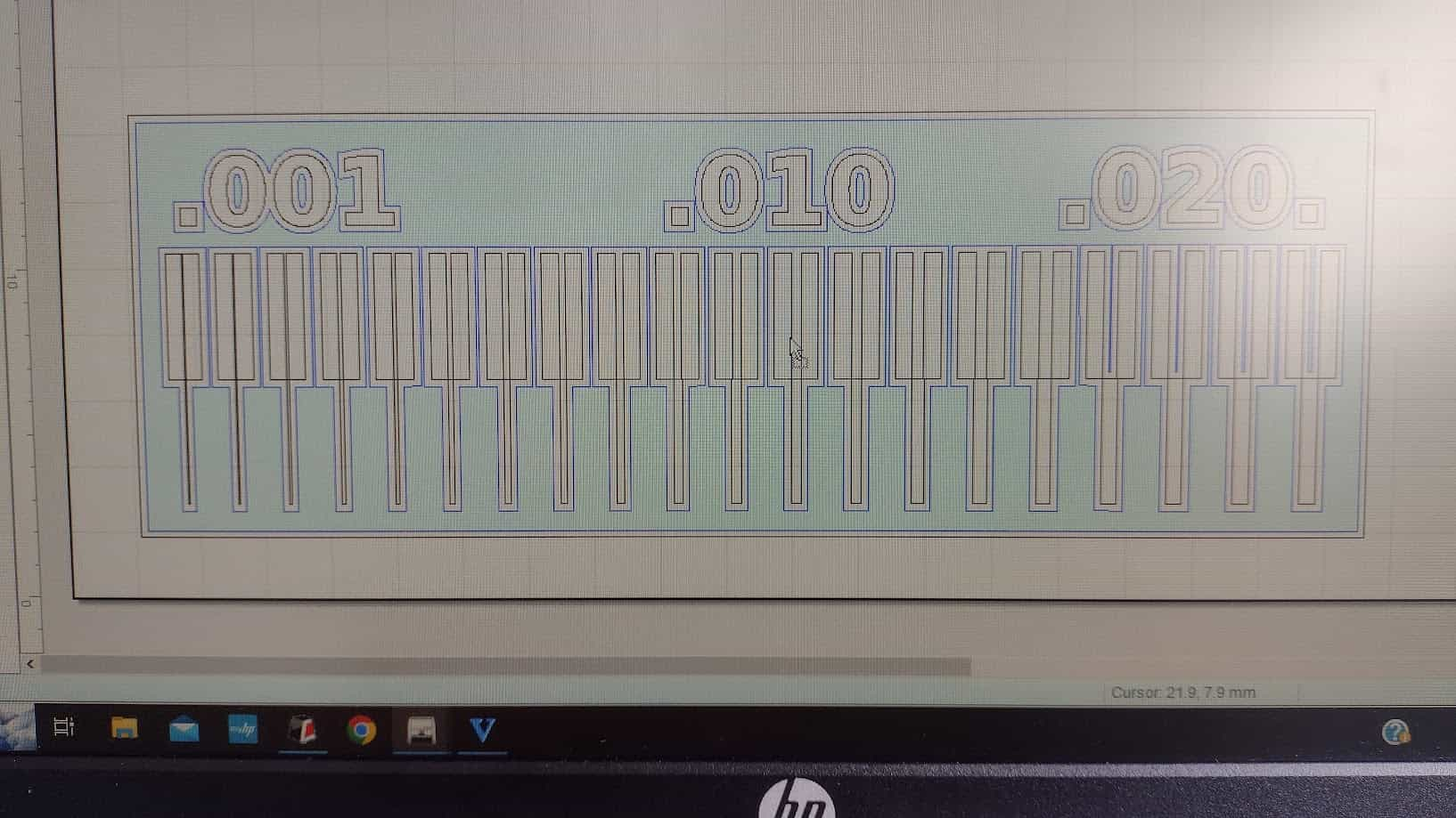
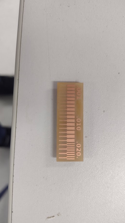
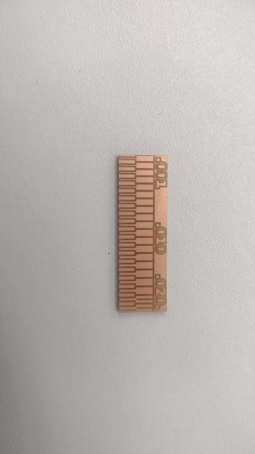
Here we can see the difference between test 7 and test 8, where we were able to achieve the objective that was requested of us for the group work. We understood the processes, configurations and were able to obtain our board test.
SENDING A PCB TO A BOARD HOUSE
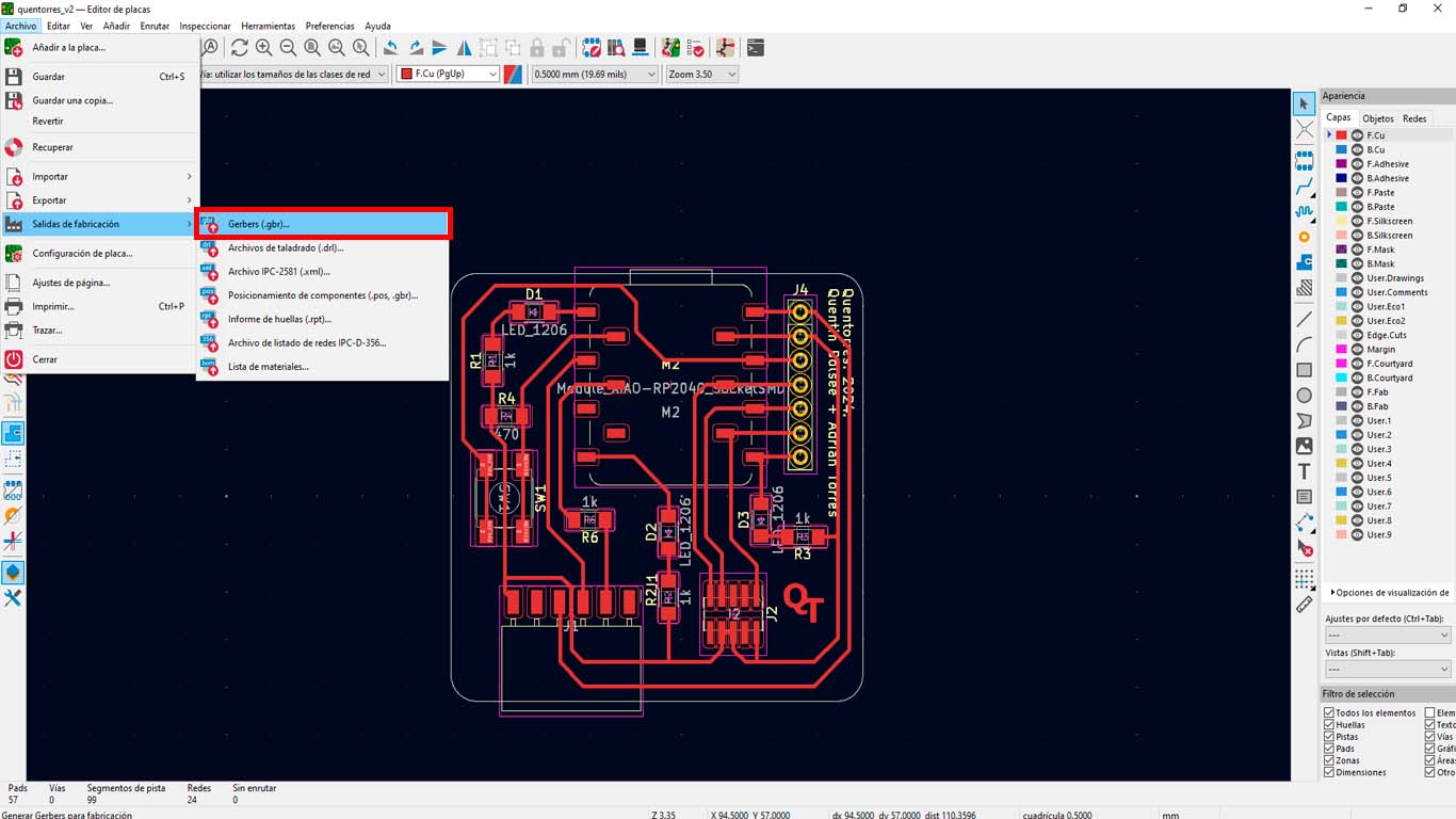
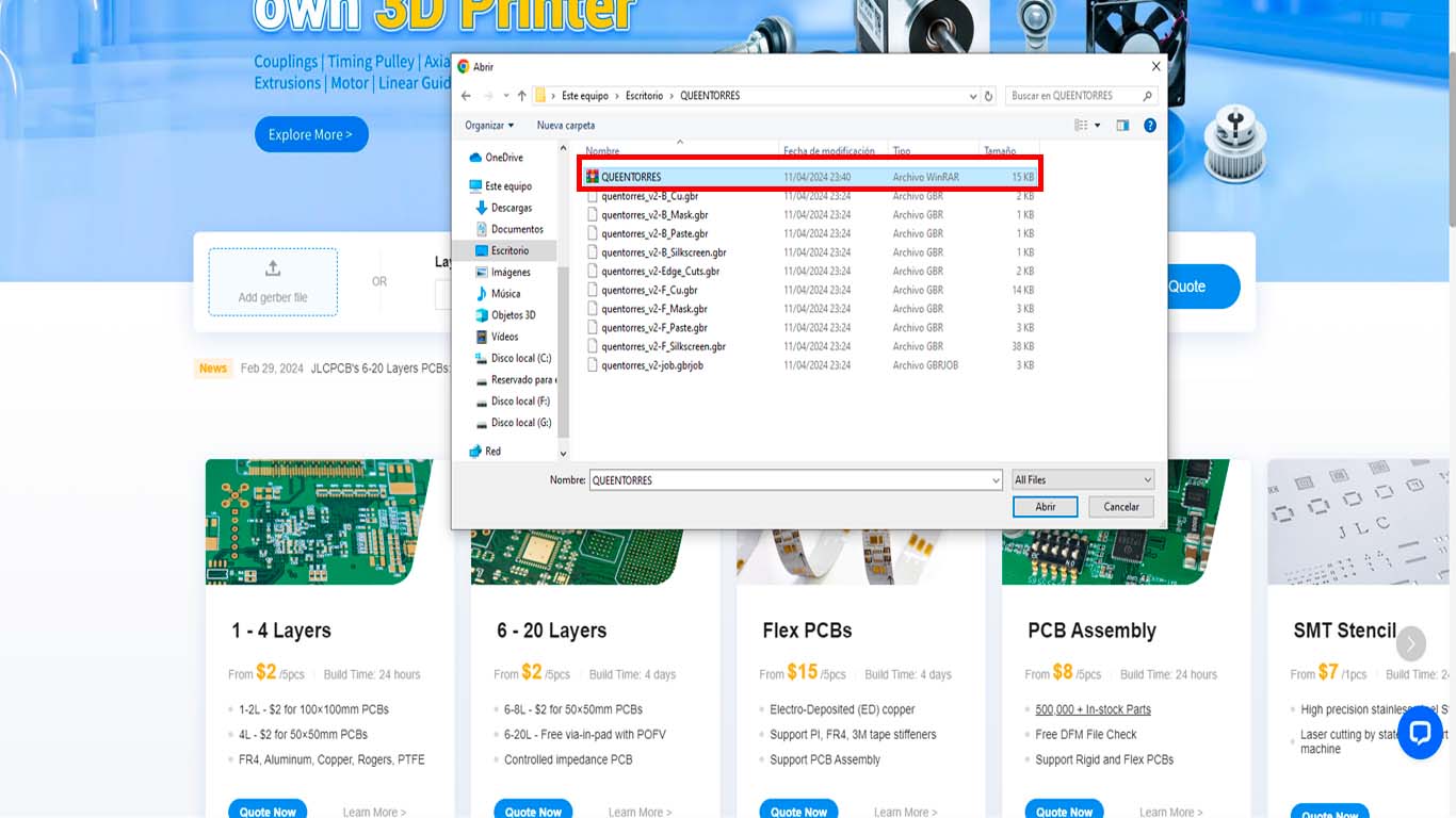
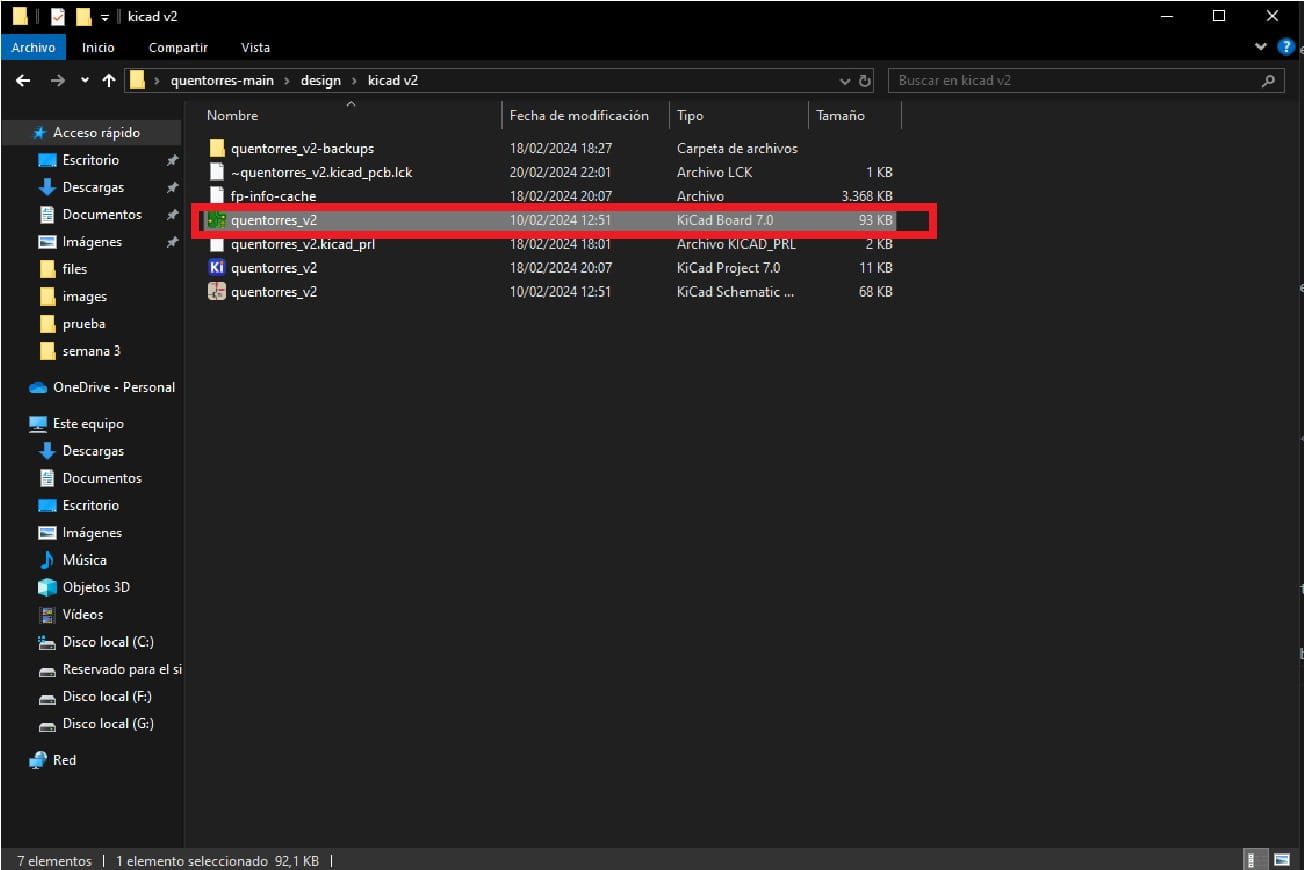
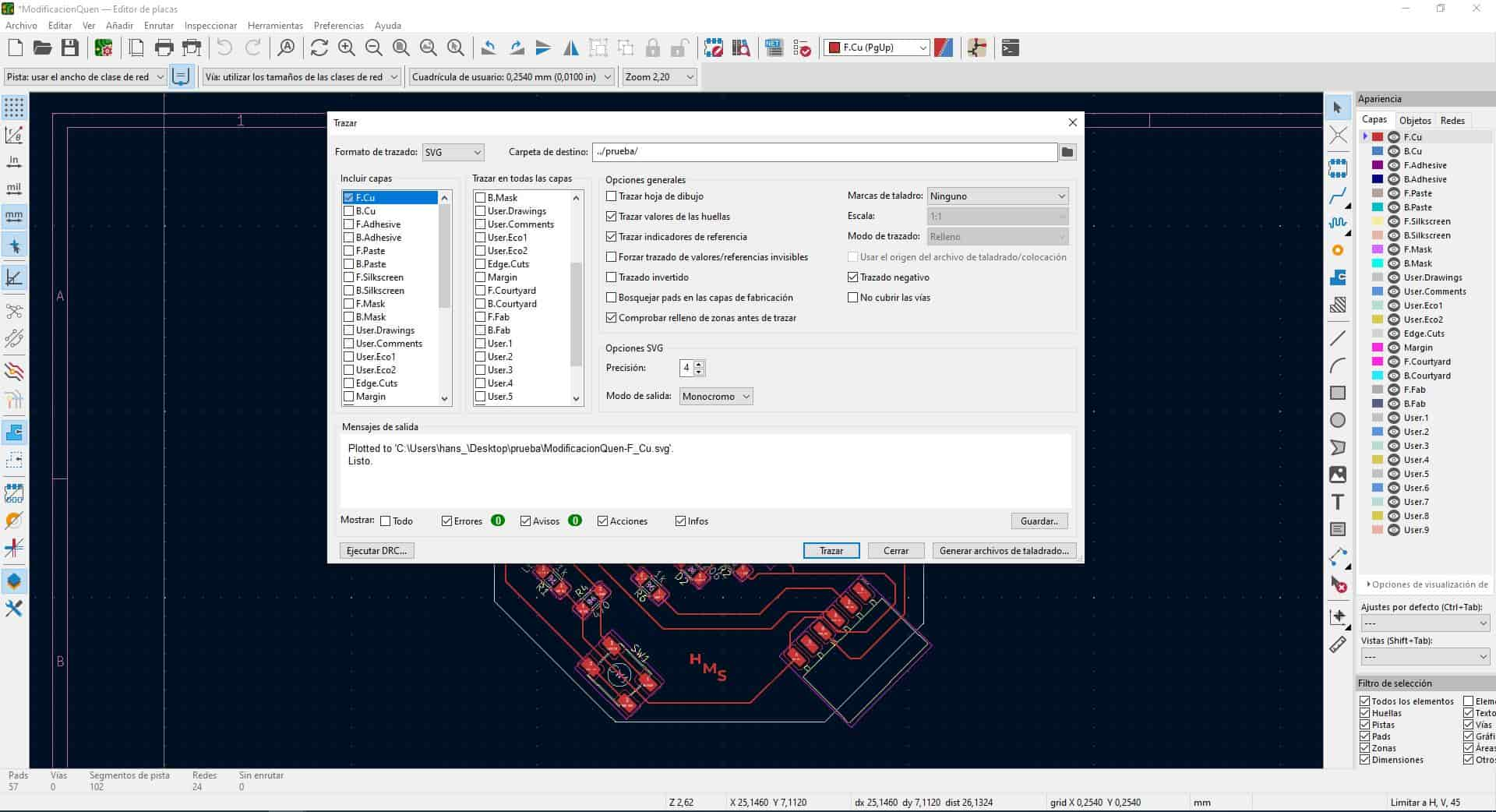
To send our plate to a BOARD HOUSE we need to export our plate design, in this case the QUENTORRES, in GERBER format, since it is a universal format where all BOARD HOUSEs work with the format to make any type of plate that one is wanting. manufacture. Here I will show the process of how in KICAD we can export in GERBER format.
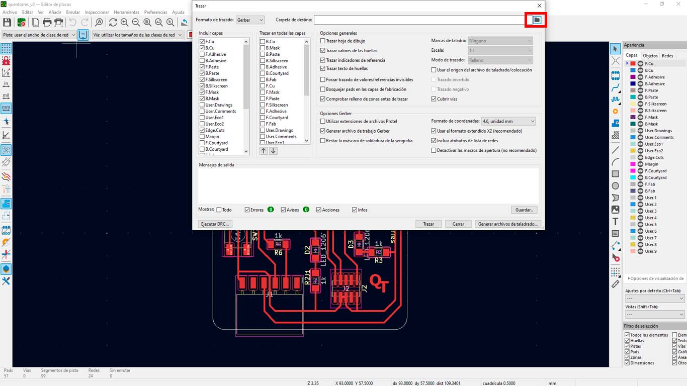
Then we go to the "folder" to save our gerber files anywhere on our PC.
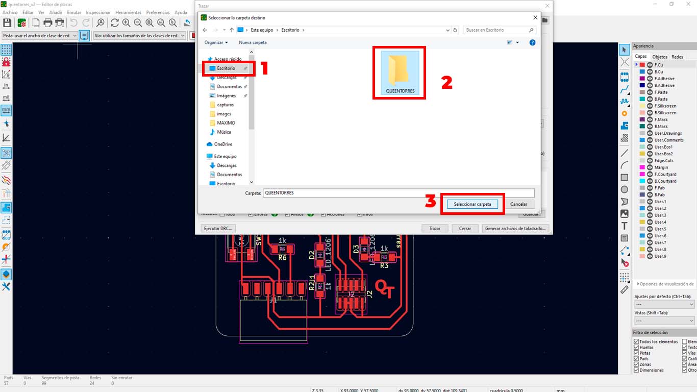
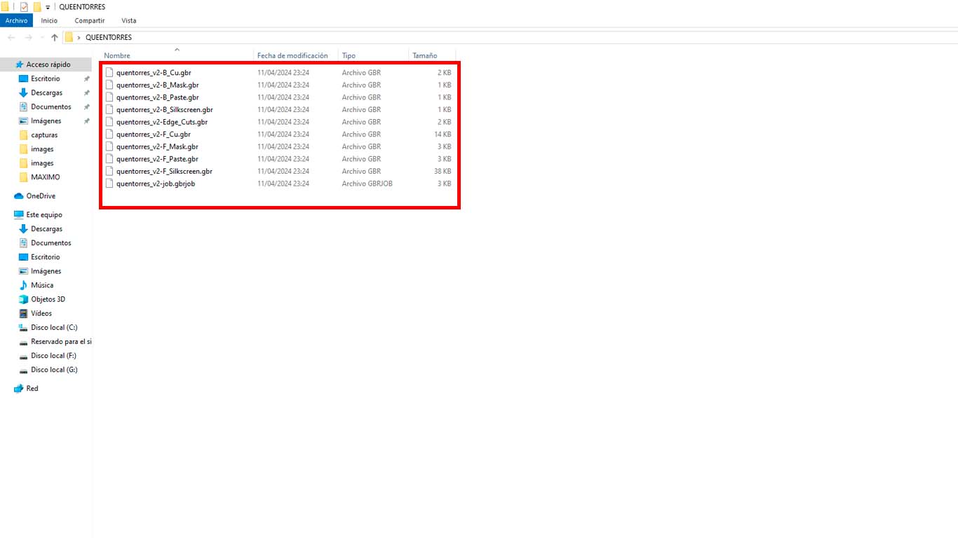
Then, on our computer we look for the place where we can save the GERBER files. In my case, I will do it on the desktop, then I will create a folder with the name QUENTORRES and I will select it. All the documents that we exported and that we will need will be saved here.
Finally, we have to select some layers so that the company where we are going to have it manufactured takes into account all the details of our card and finally we click on PLOT.
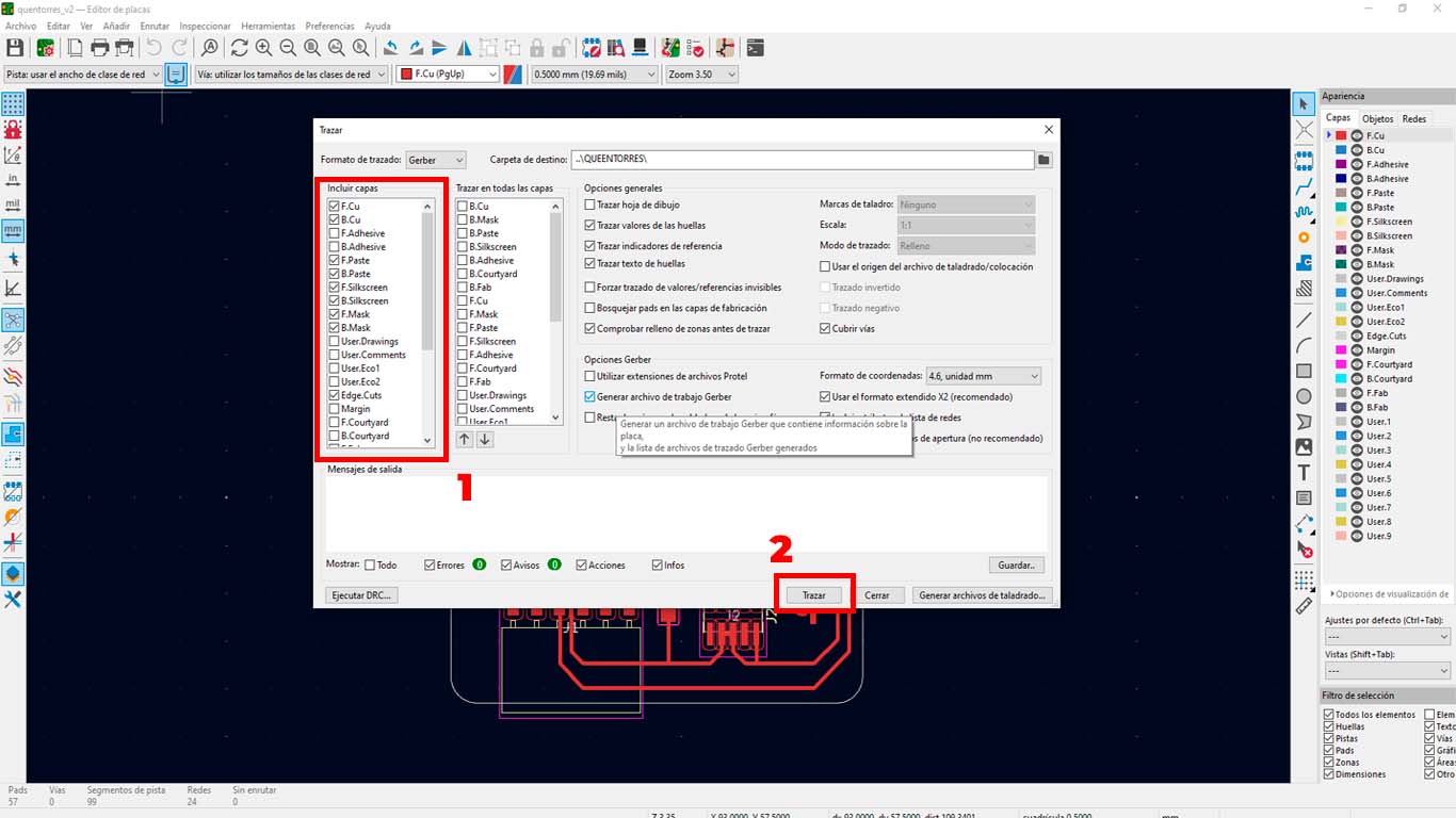
Then we check our folder where we export the GERBER format and we can see all the layers and each one with its file.
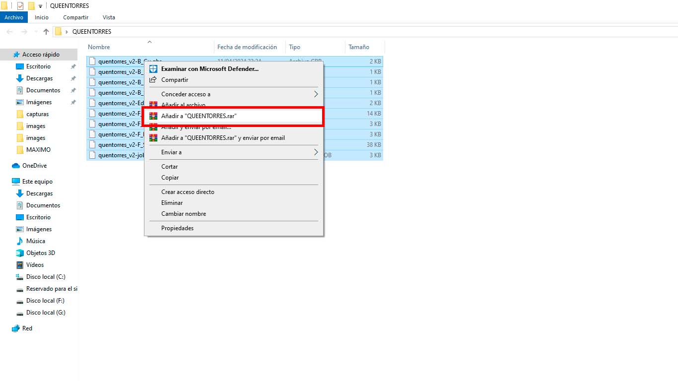
To send to a company, we have to do it in RAR format or ZIP format. It can be any of the two and let's remember that they must have all the files that KICAD gives us.
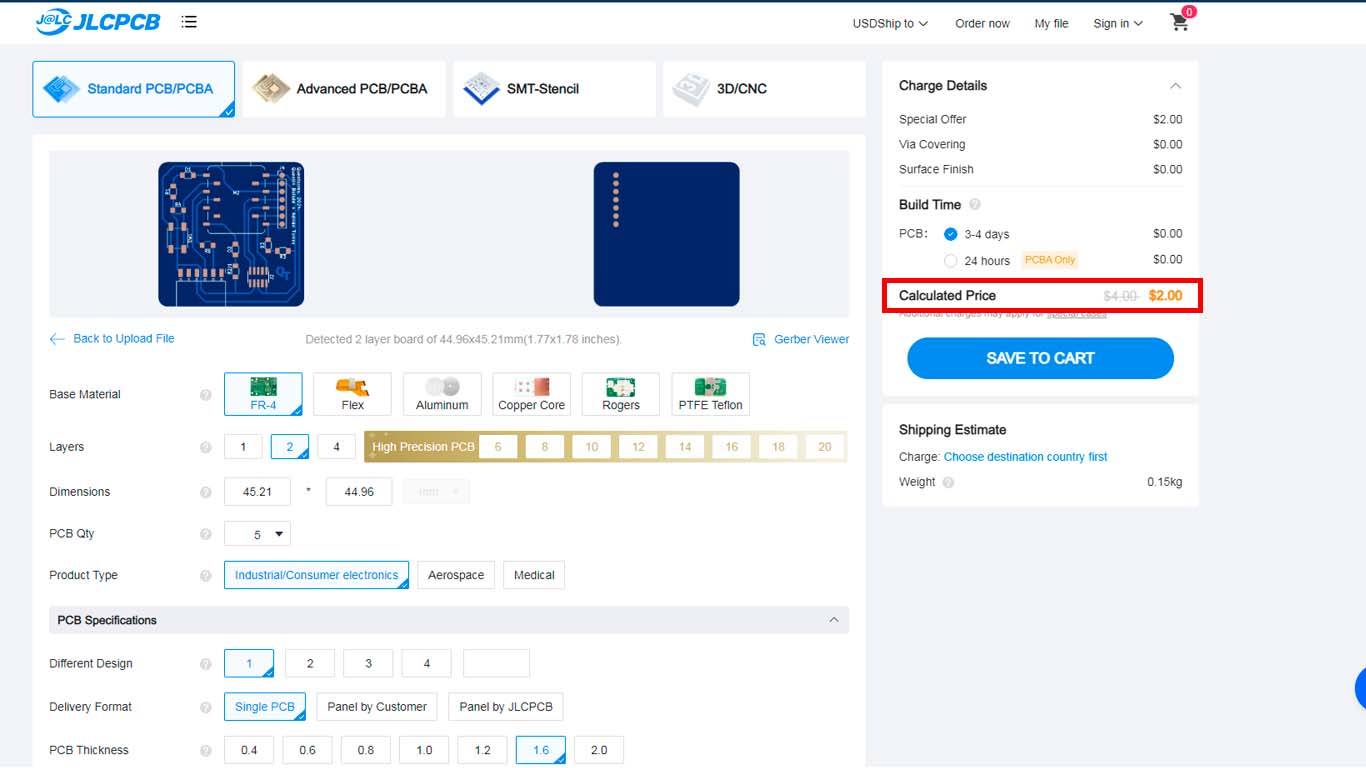
For this example and on the recommendation of some instructors, we will send it to the JLCPCB company to be able to send the card.
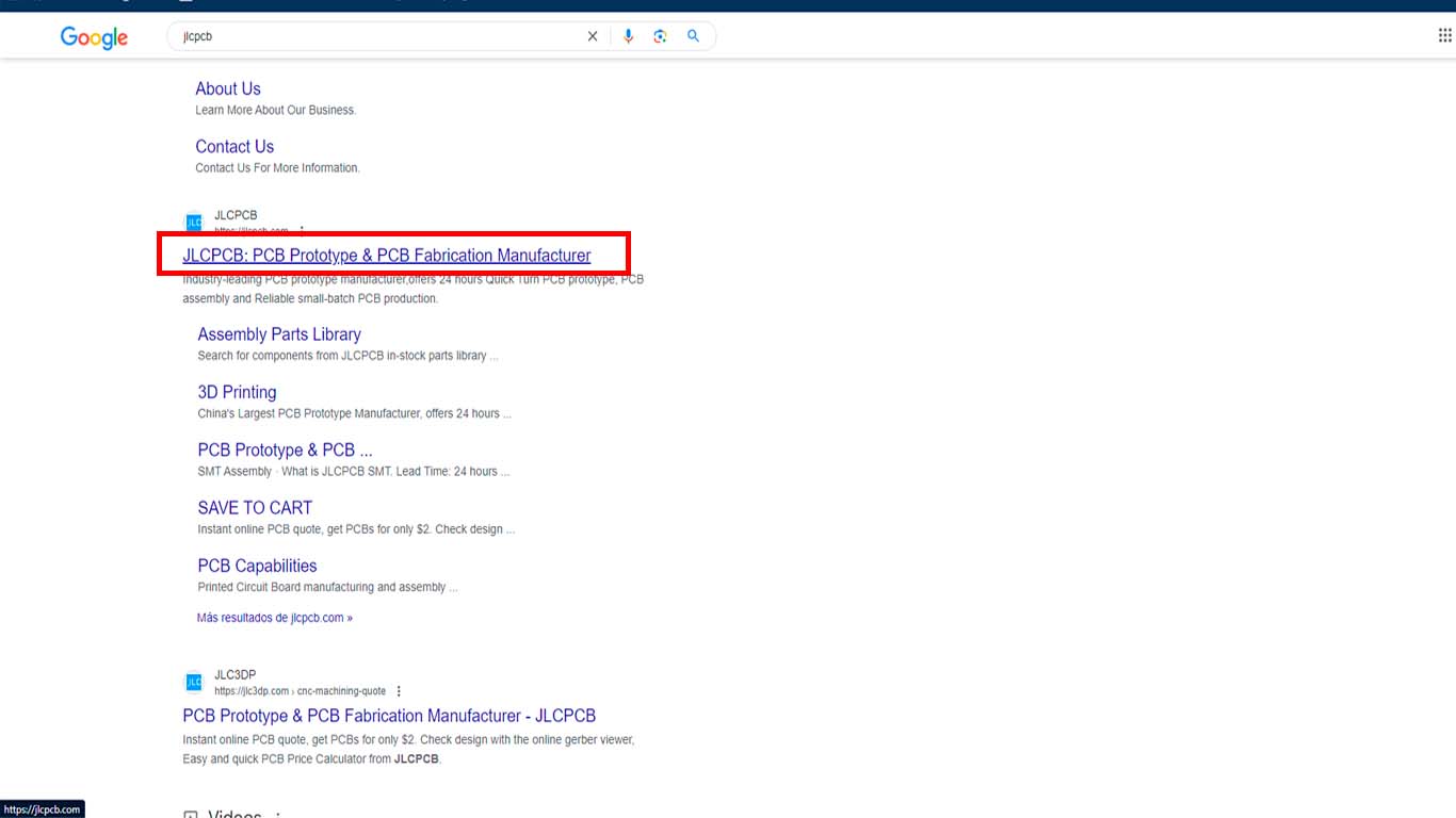
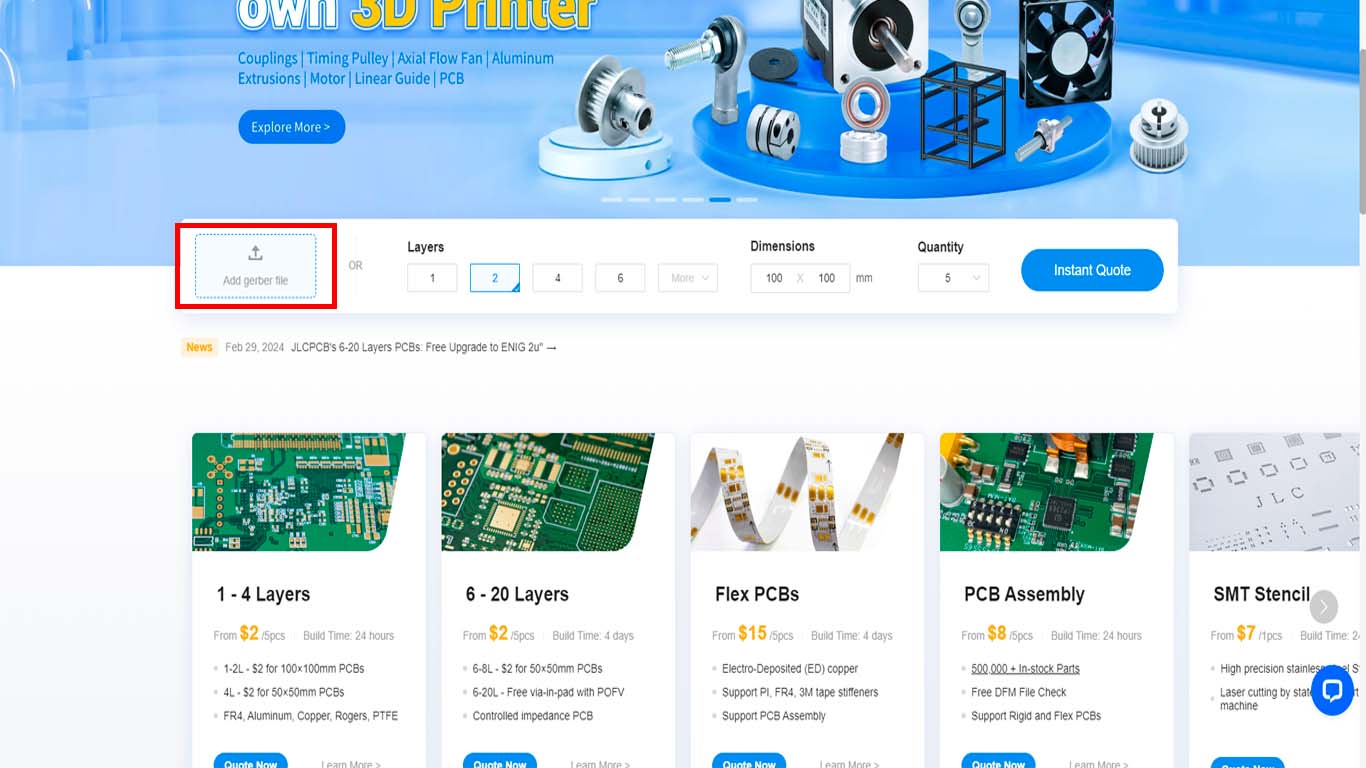
Then we navigate through the company page, and we go to GERBER FILE and this is where we load our RAR that we export from KICAD where all the layers of QUENTORRES are.
It will load a new window where we can see the characteristics of our plate, in this case the QUENTORRES would cost 2 dollars. Now we will see how much the shipping is to my country, Peru.
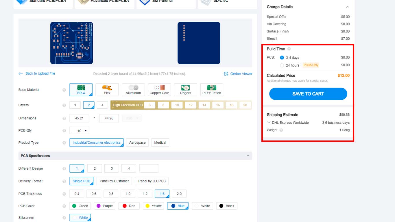
After entering our country and the details such as the quantity, color and other services we want. We can realize that the shipping of the plate and the total cost reaches approximately 90 dollars to Peru. And this is how it is sent to any PCB manufacturing company when we want to manufacture a large number of boards.
INDIVIDUAL ASSIGNMENT
MAKE AND TEST MICROCONTROLLER DEVELOPMENT BOARD
SETUP AND MILLING - QUENTORRES
MILLING WITH iMODELA CREATOR SOFTWARE
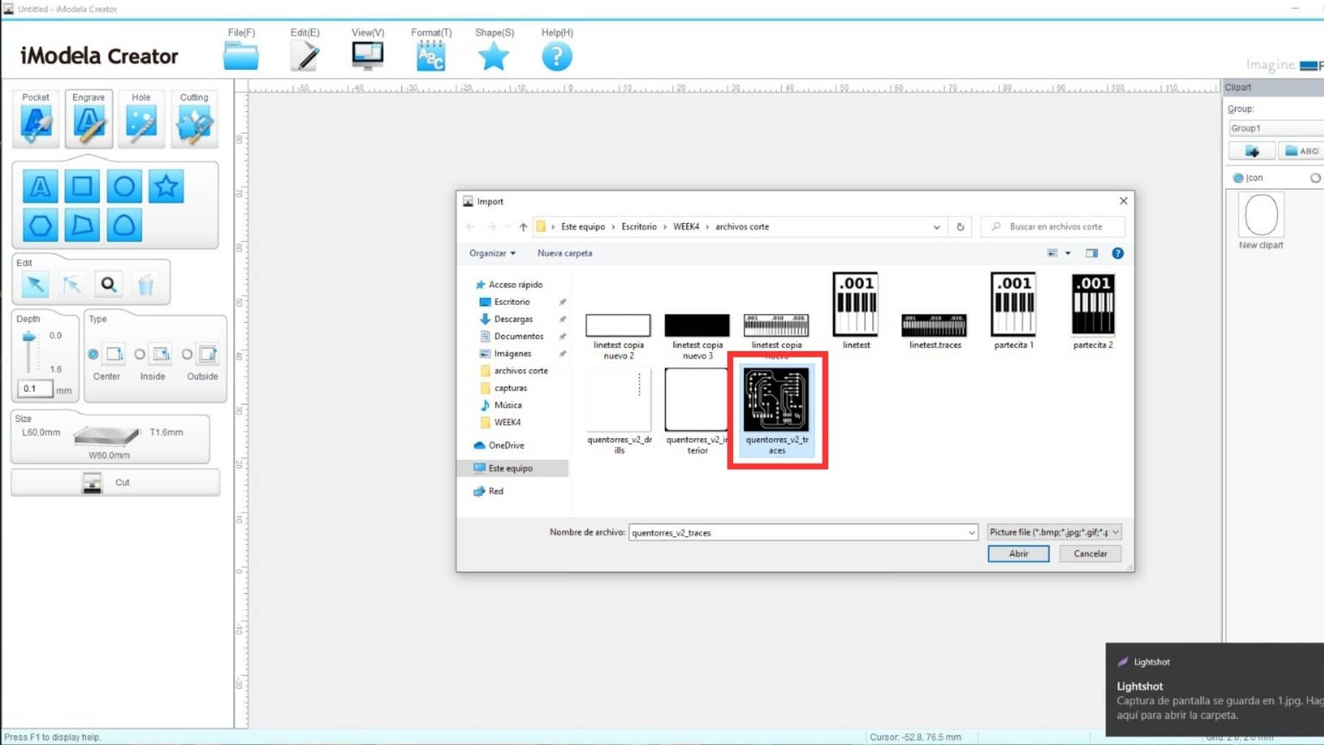
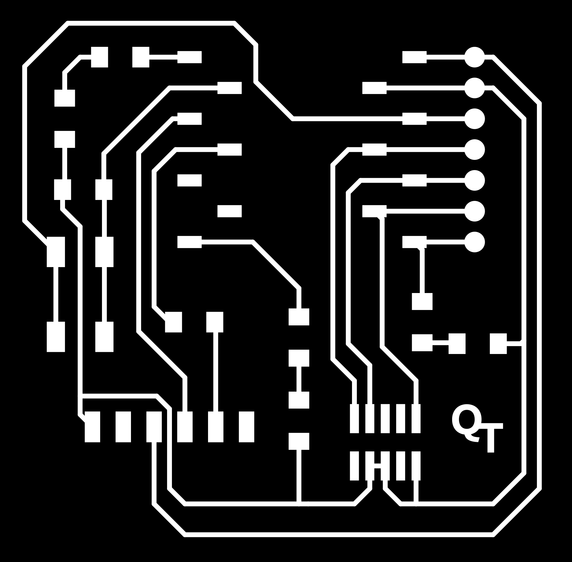
I decided to use 2 programs, I will start by explaining my experience with iMODELA CREATOR , which is a MONOFAB program to perform milling. In this section we will see how the microcontroller board was made with this program. First we have to get the PNG images of the plate in 3 layers: DRILLS, INTERIOR and TRACES.
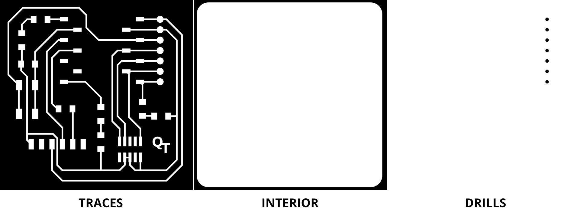
After that, we started importing the TRACES to start making the board. To do this, in the IMODELA CREATOR program we import the trace file.
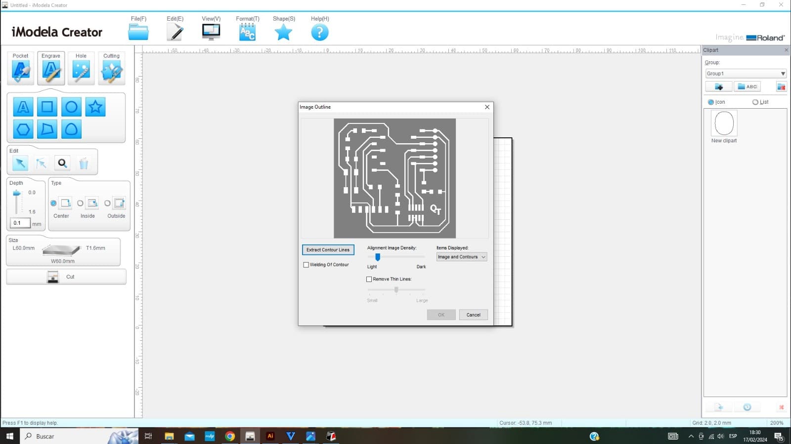
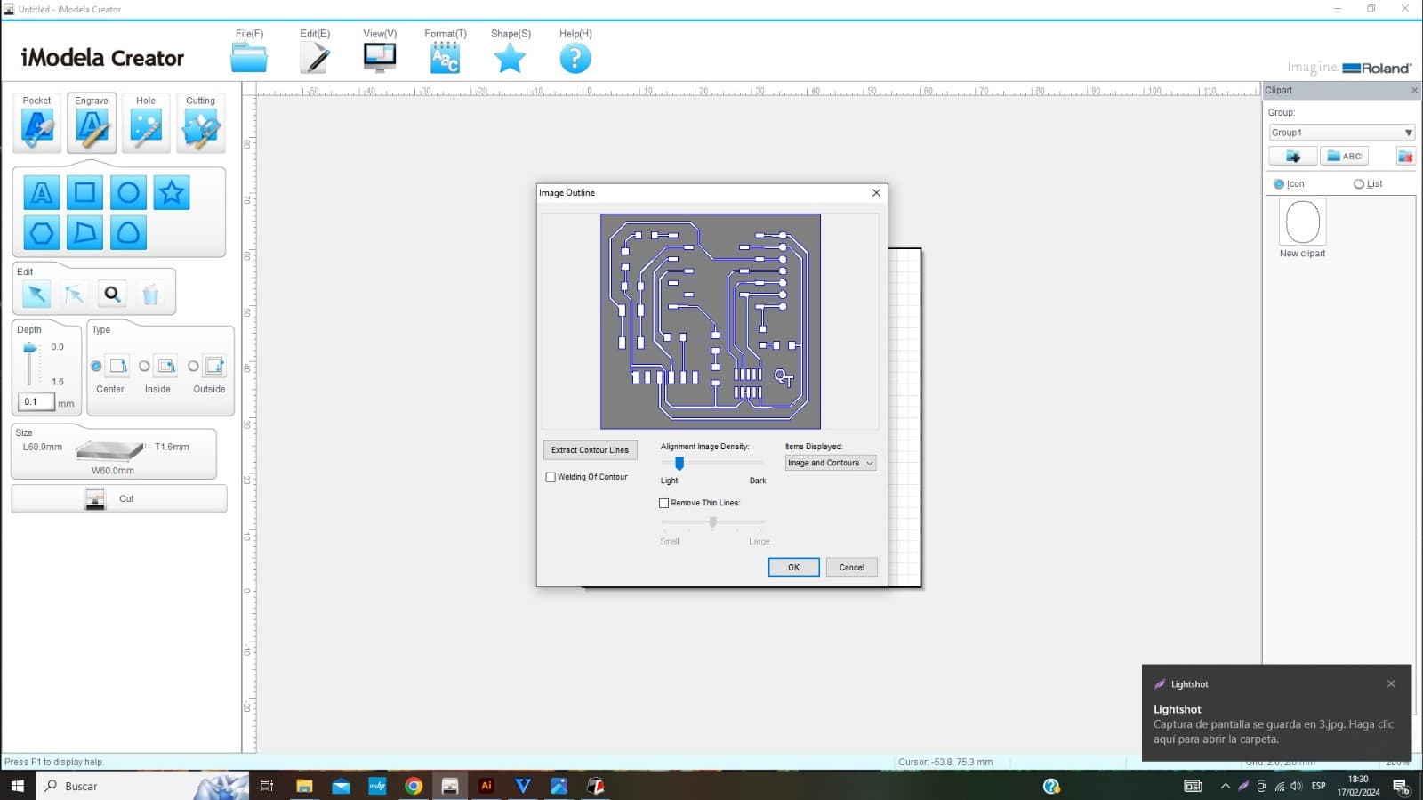
Then the program will allow us to VECTORIZE the PNG to find the traces that we are going to make, by clicking on "EXTRACT CONTOUR LINES", we obtain the lines that are marked in the preview and by clicking on "OK"we can obtain the plate in the program.
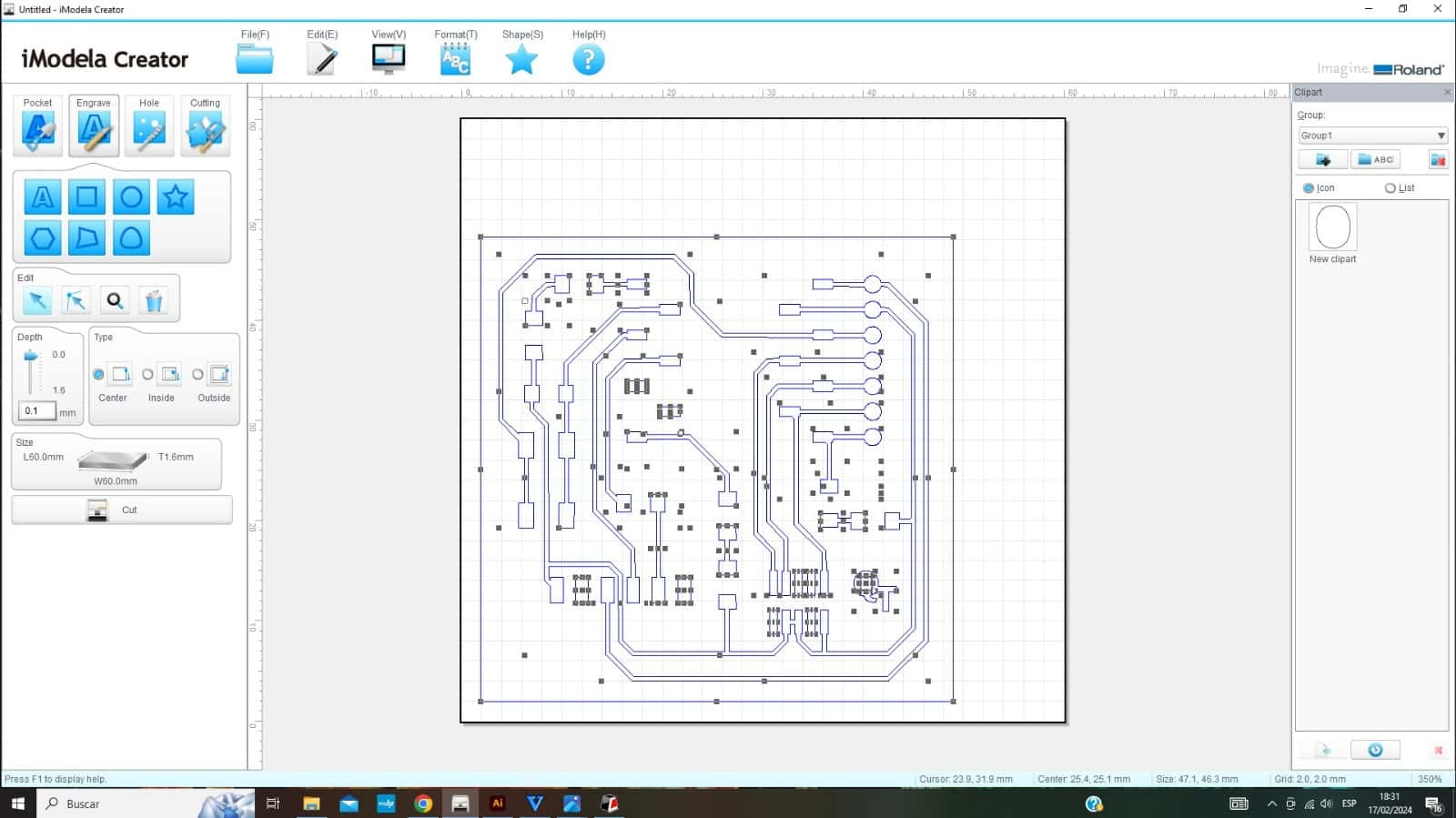
Now we configure the characteristics of the plate that we are going to work on, it is important to set the thickness of the plate and the thickness of what we are going to mill since it is not necessary to mill very deep.
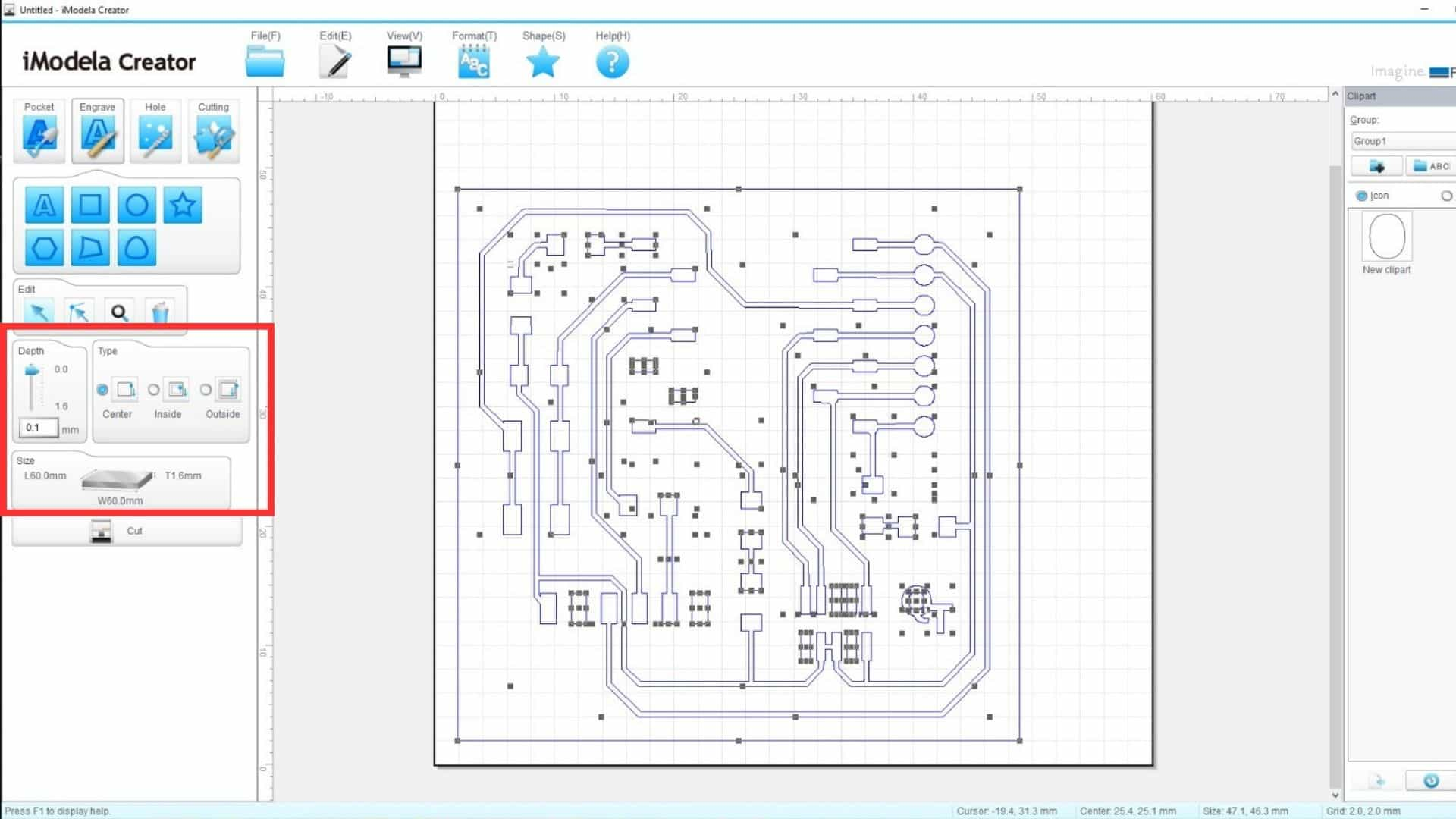
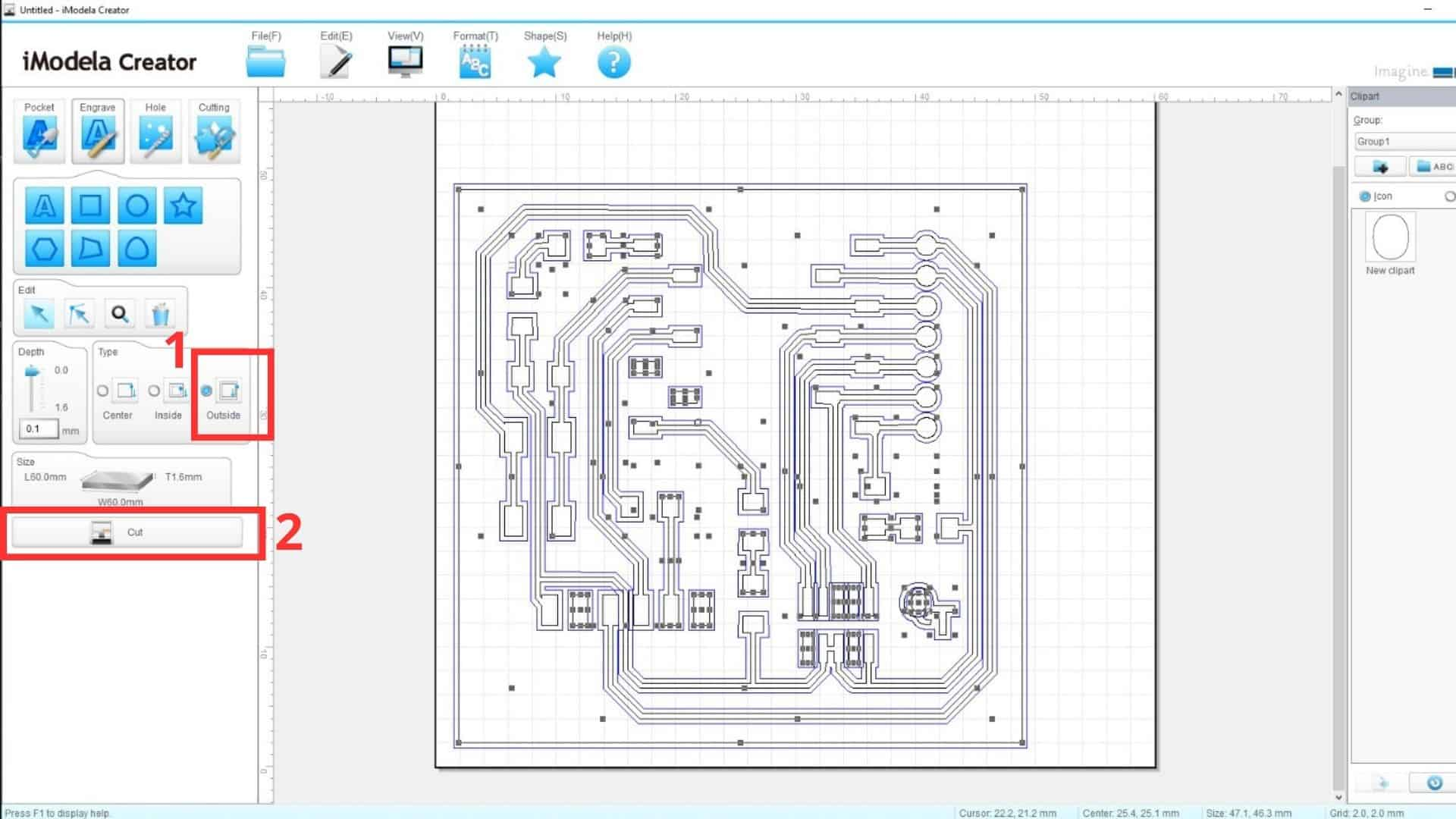
Then we click on the OUTSIDE button since it is important for the drill bit to do its work outside of the TRACES that we want to make, otherwise we will make the same mistakes that were made with the milling test. And finally, we click on CUT , where we will configure the cutting speed, thickness and passes.
A window will appear where we will have to configure the type of cut and the milling diameter. Here it is super important since for the TRACES we will use the 1/64" - 0.39 mm drill bit to be able to obtain a good detail on the plate.
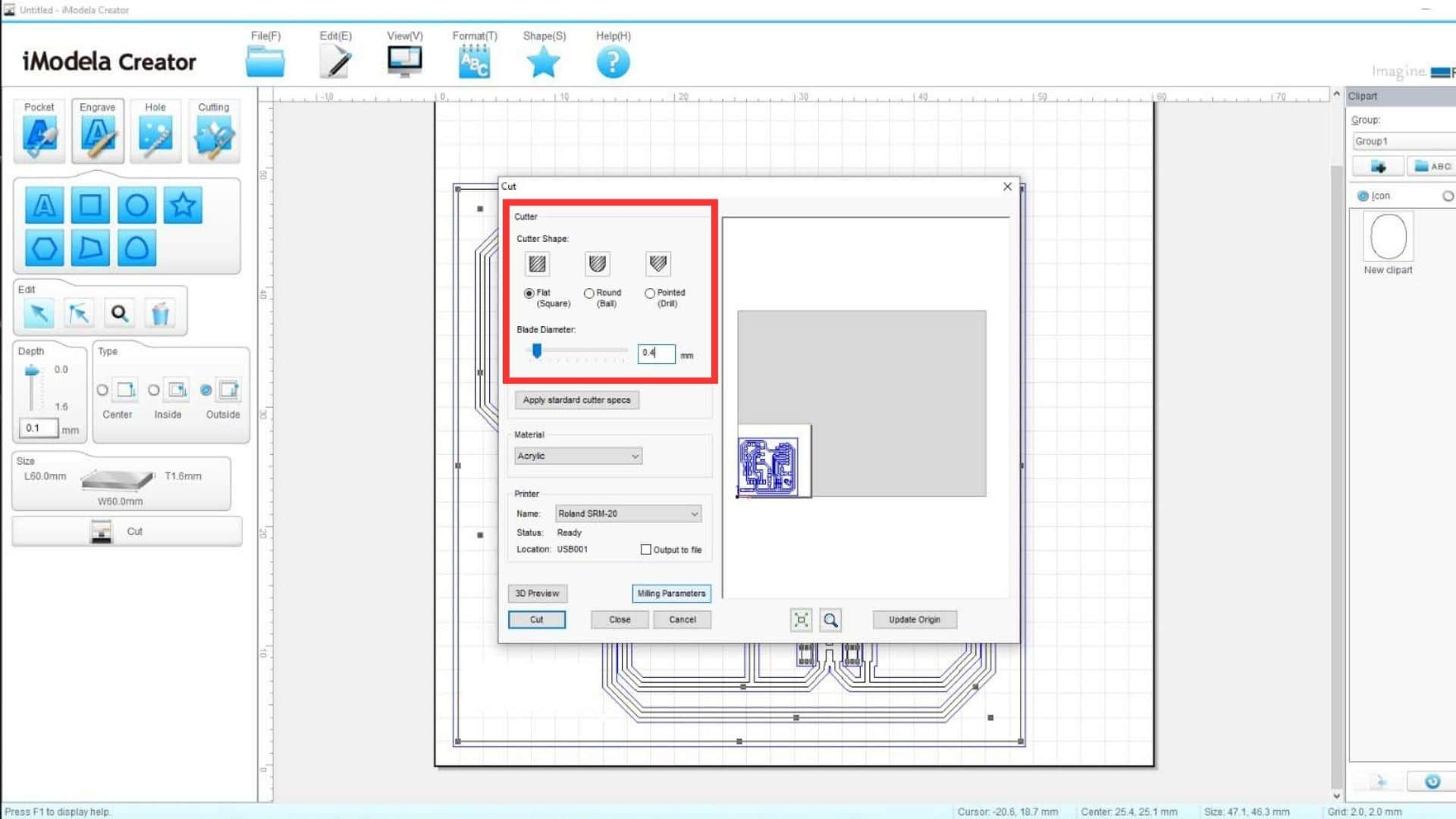
Subsequently, we click on the "MILLING PARAMETERS" button where a window will appear where we have to configure the cutting speed, the number of passes and save the configuration.
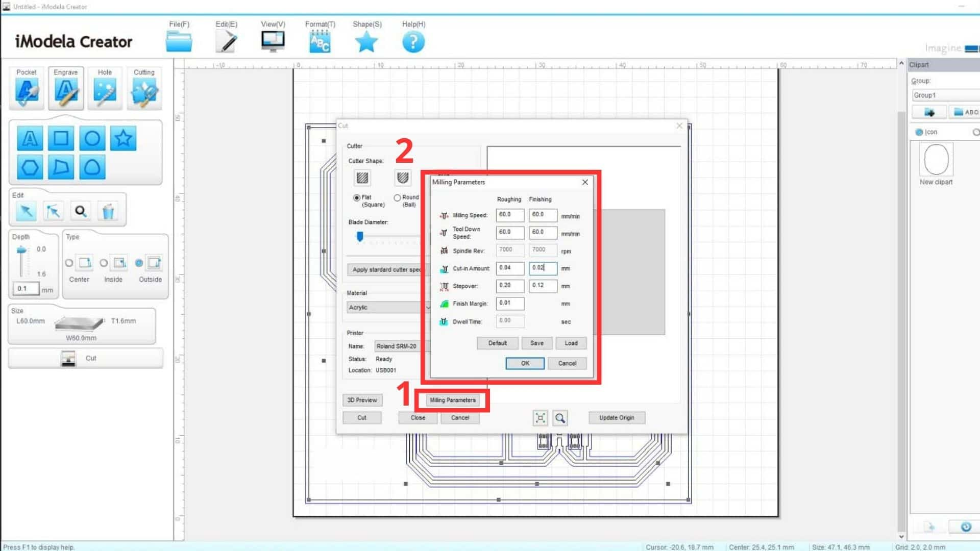
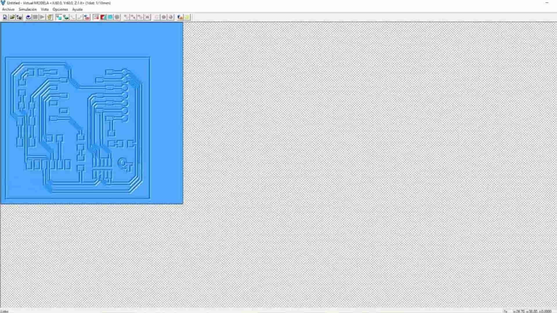
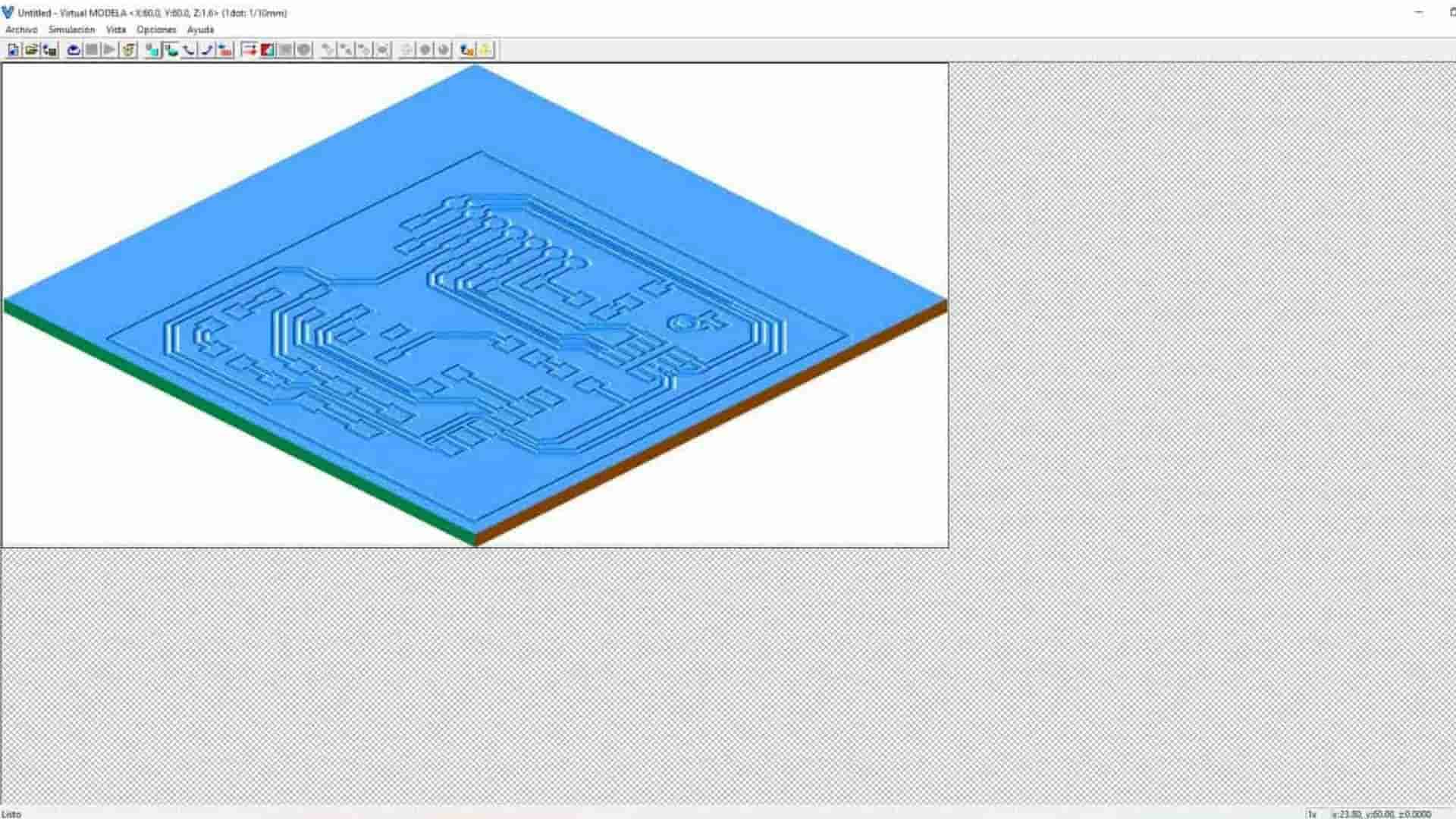
Then we will have some 2D and 3D simulations of how the work will turn out, we check that everything is fine and the traces do not suffer any cuts from the drill bit.
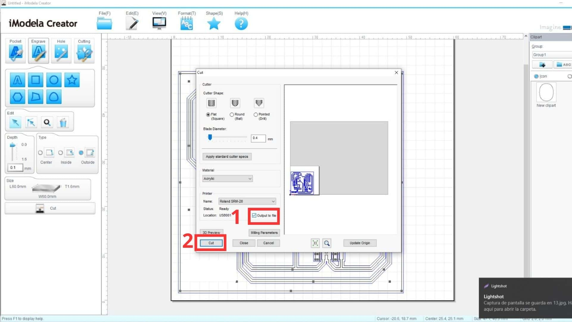
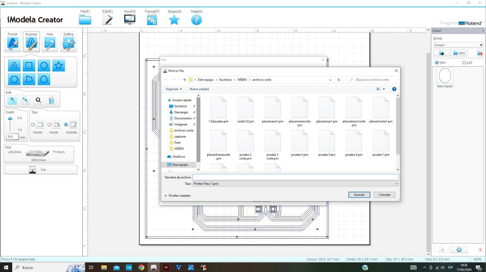
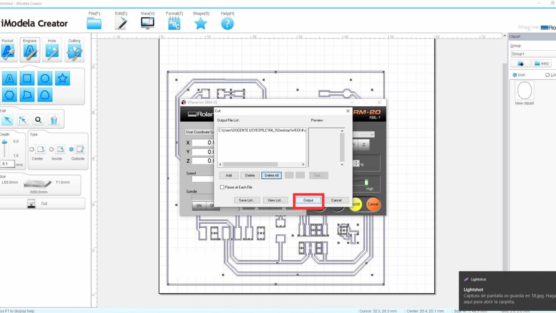
We activate the "OUTPUT TO FILE" option to prevent the machine from cutting directly and we can avoid any accident or the bit breaking. Then, we click on the "CUT" button, which will open a window to save the cut file and configure it from the MONOFAB software.
Then we save the file that saves the file that we are going to cut and we will open it with the MONOFAB program
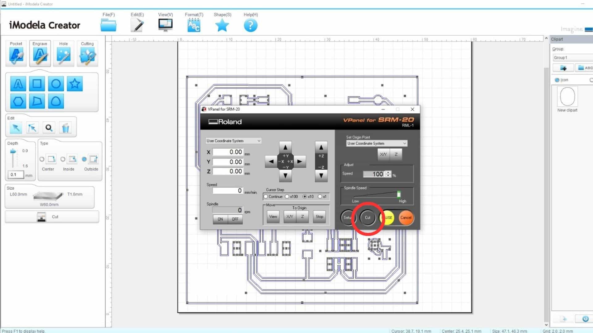
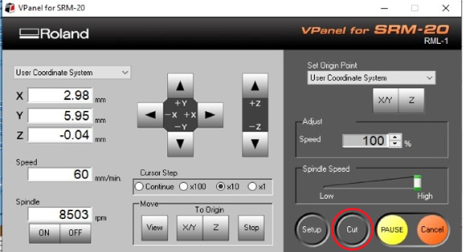
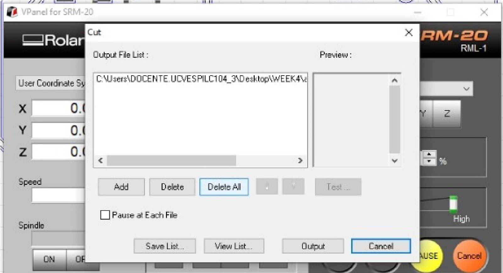
Now we enter the monofab software and click on "CUT" . A window will open where we will have to enter "DELETTE ALL" to delete old jobs that were carried out and click on "ADD" .
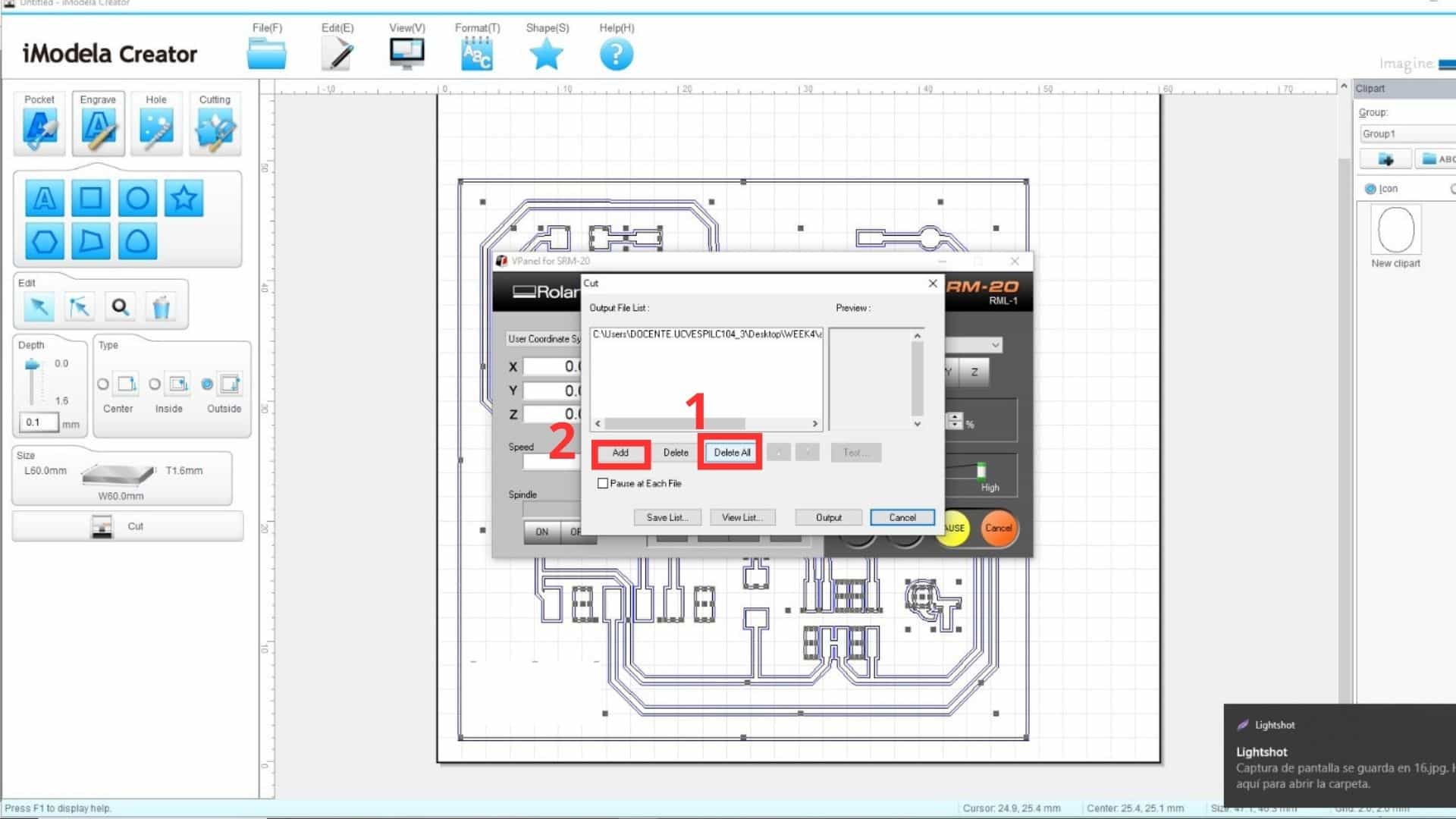
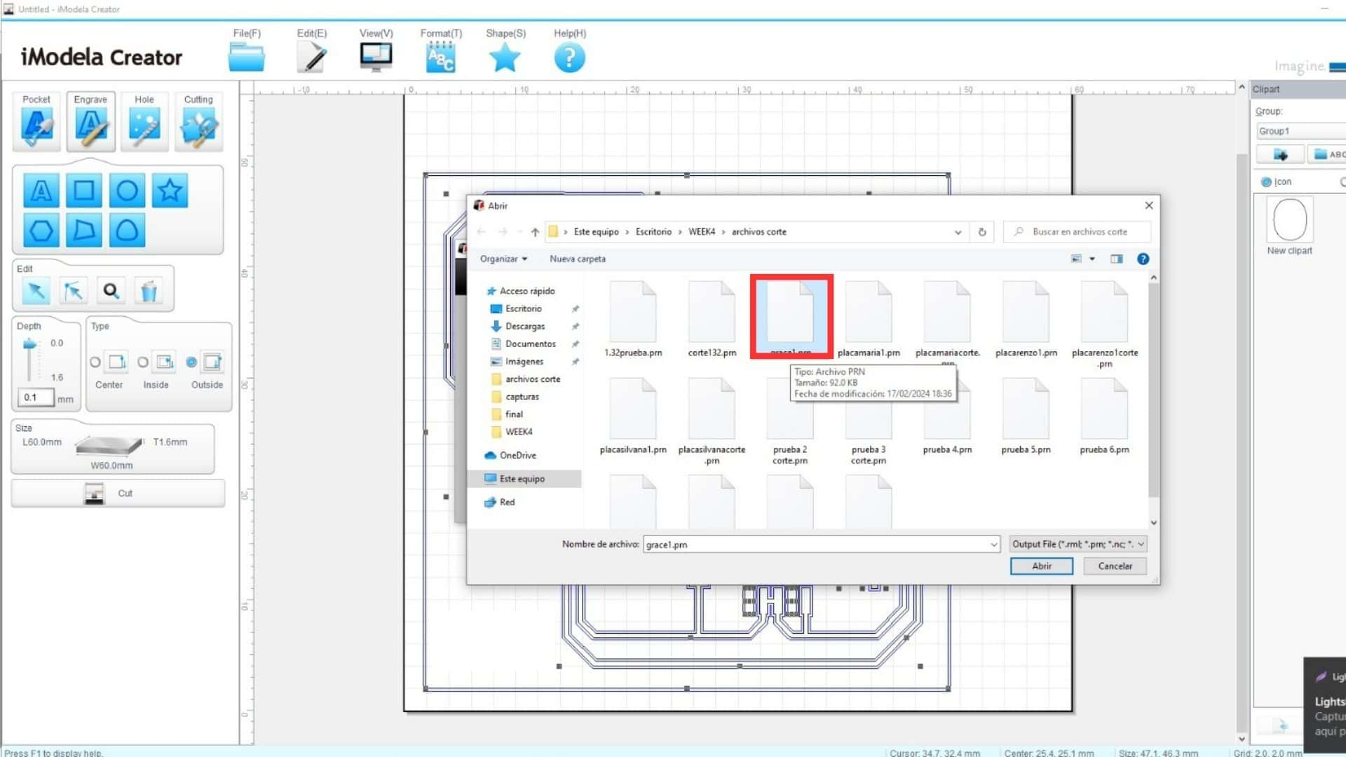
We select the file that we saved previously and click on "OPEN" and the window will close. So we finally click the "OUTPUT" button where the machine will start cutting the job.
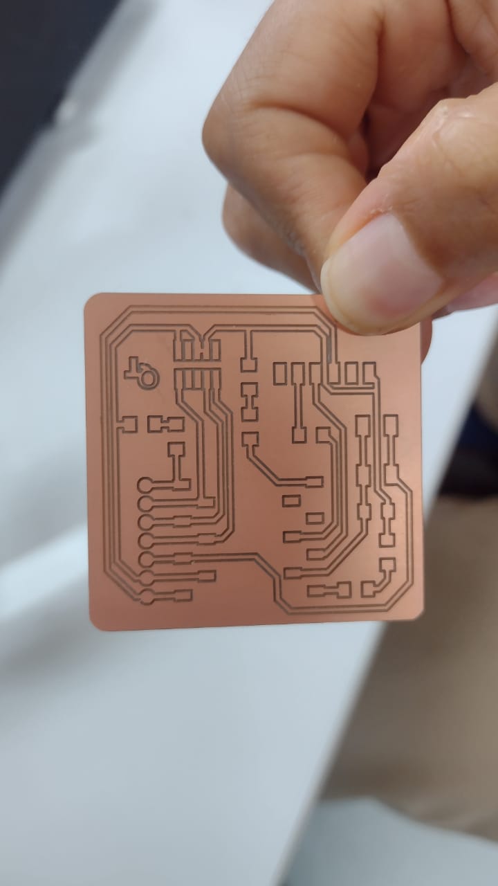
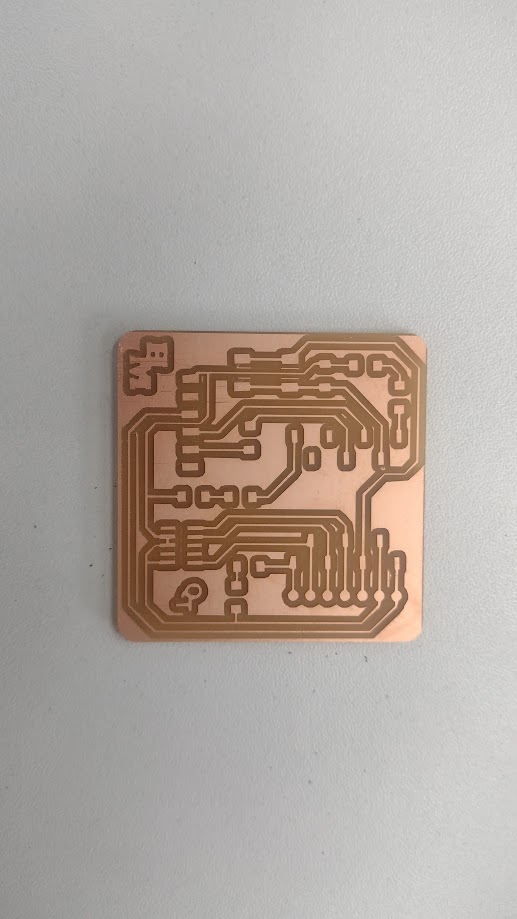
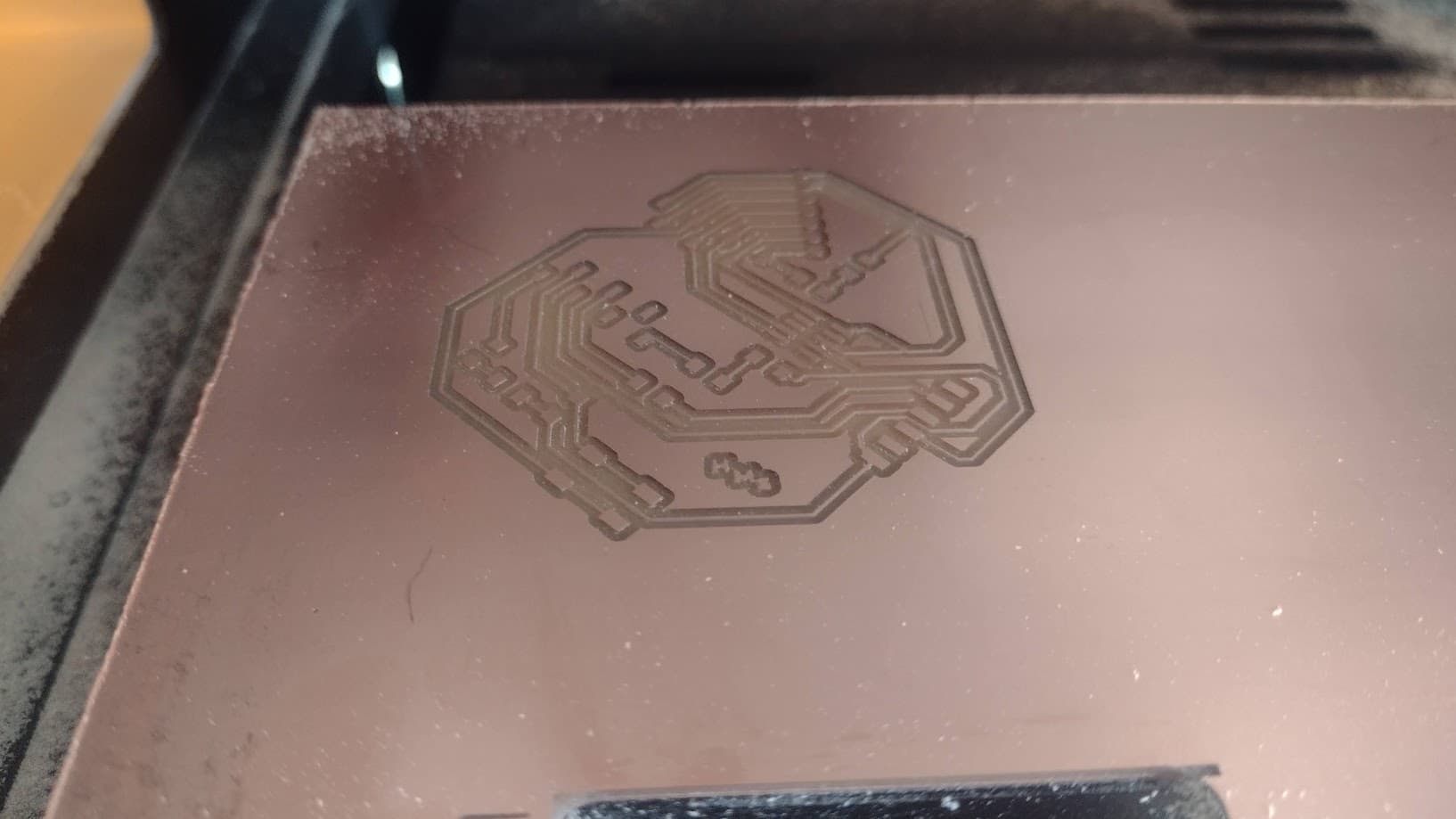
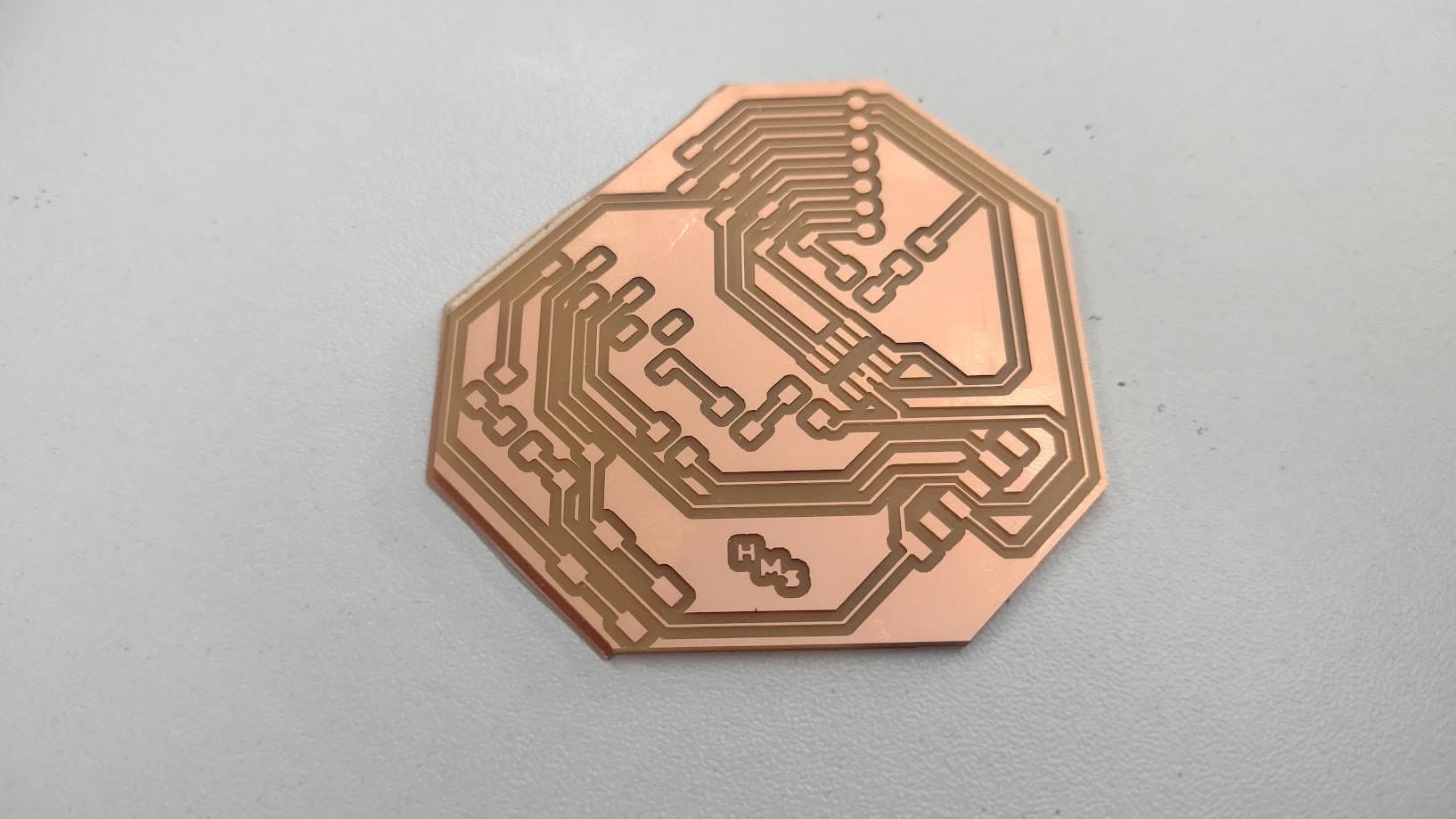
Here we can see the result of the milling and cutting of the plate in the MONOFAB. It went very well except that they gave us a recommendation for the OFFSET of the TRACES, these should be wider, however until that day, Saturday 02/17/2024, we could not resolve it
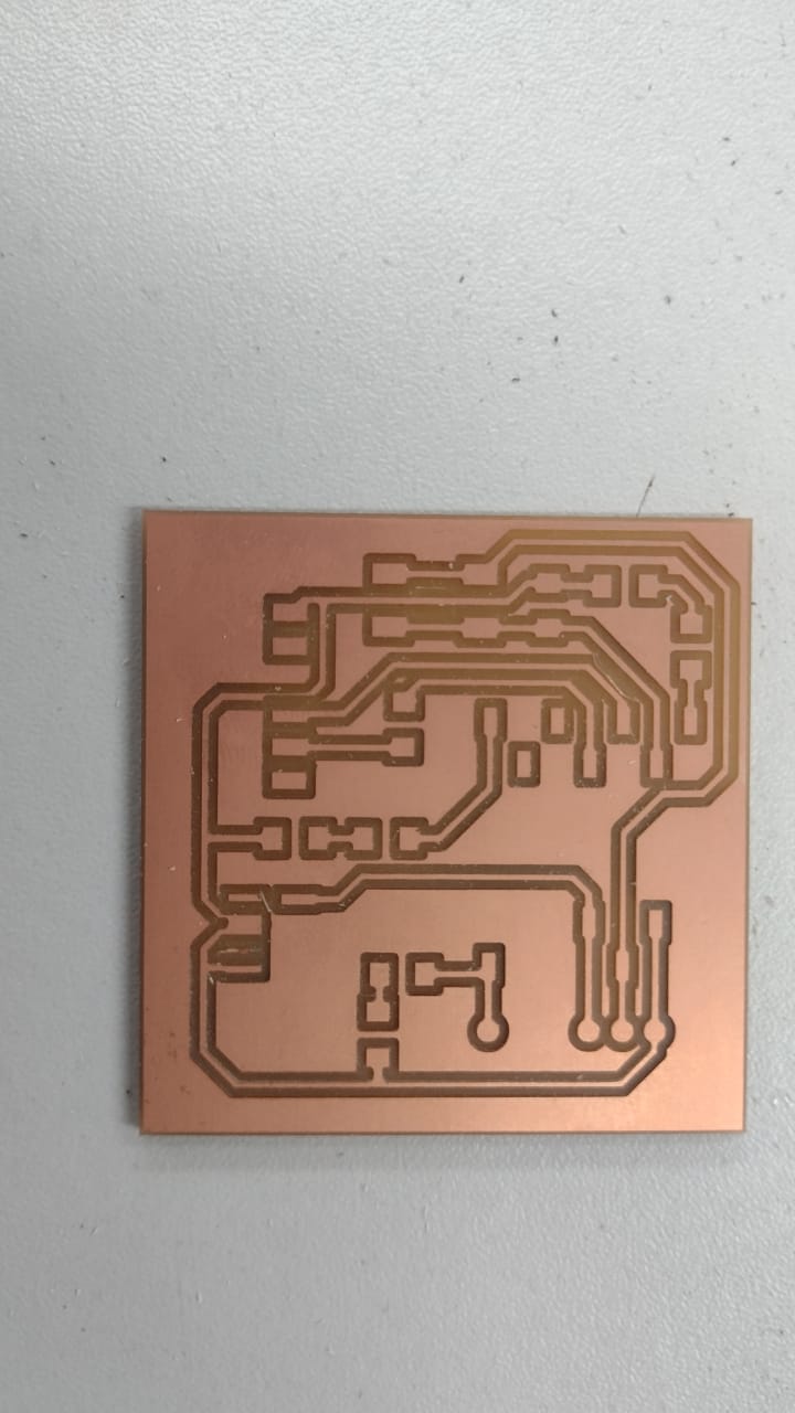
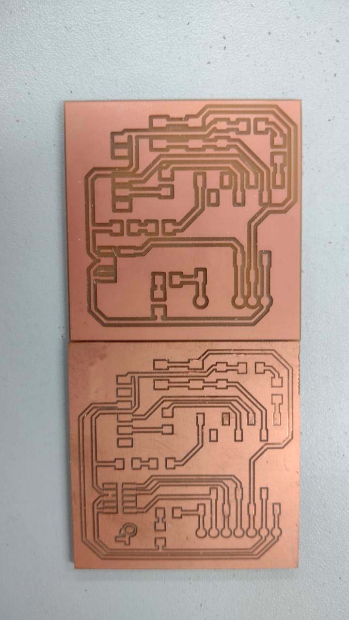
We couldn't find a way to enlarge the milling with the 1/64" drill bit, so we decided to carry out the test with the 1/32" drill bit, if possible, however, in the very close TRACES it is very complicated because it mills the traces that it should not pass. . Here you can see a photograph of what the difference looks like.
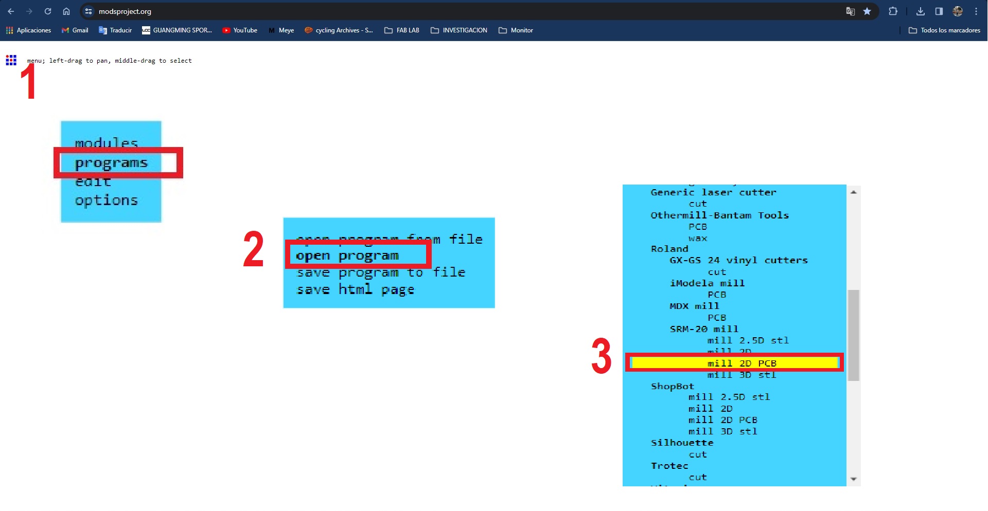
MILLING WITH MODSPROJECT.ORG WEBSITE
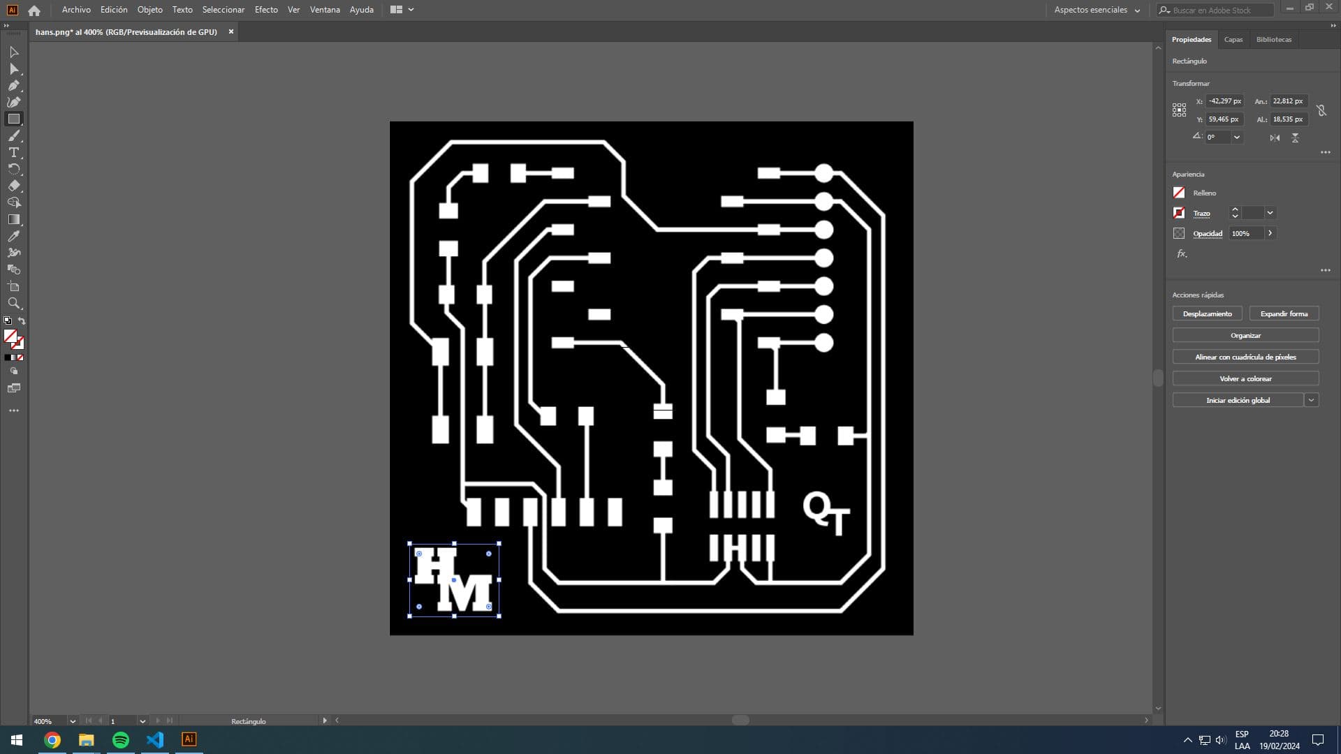
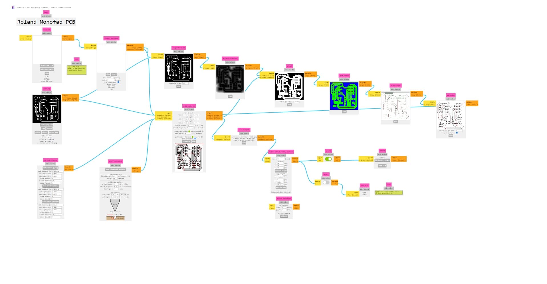
For this second test we will use MODSPROJECT.ORG, which is a page that gives us all the information that MONOFAB needs to make cuts from PNG or SVG files. In this case, we will work with the QUENTORRES PNG file, where I added my initials of my name in ILLUSTRATOR.
Then save or export the file in PNG and in our reliable browser we search for the following website "modsproject.org" . Where we can start configuring our cut.
We right click and choose the "PROGRAMS" option, then "OPEN PROGRAM" and in the next box we look for the "SRM- 20 MILL" option and choose the one that says "MILL 2D PCB"
We will get the following "TREE" where by default everything is configured according to our needs.
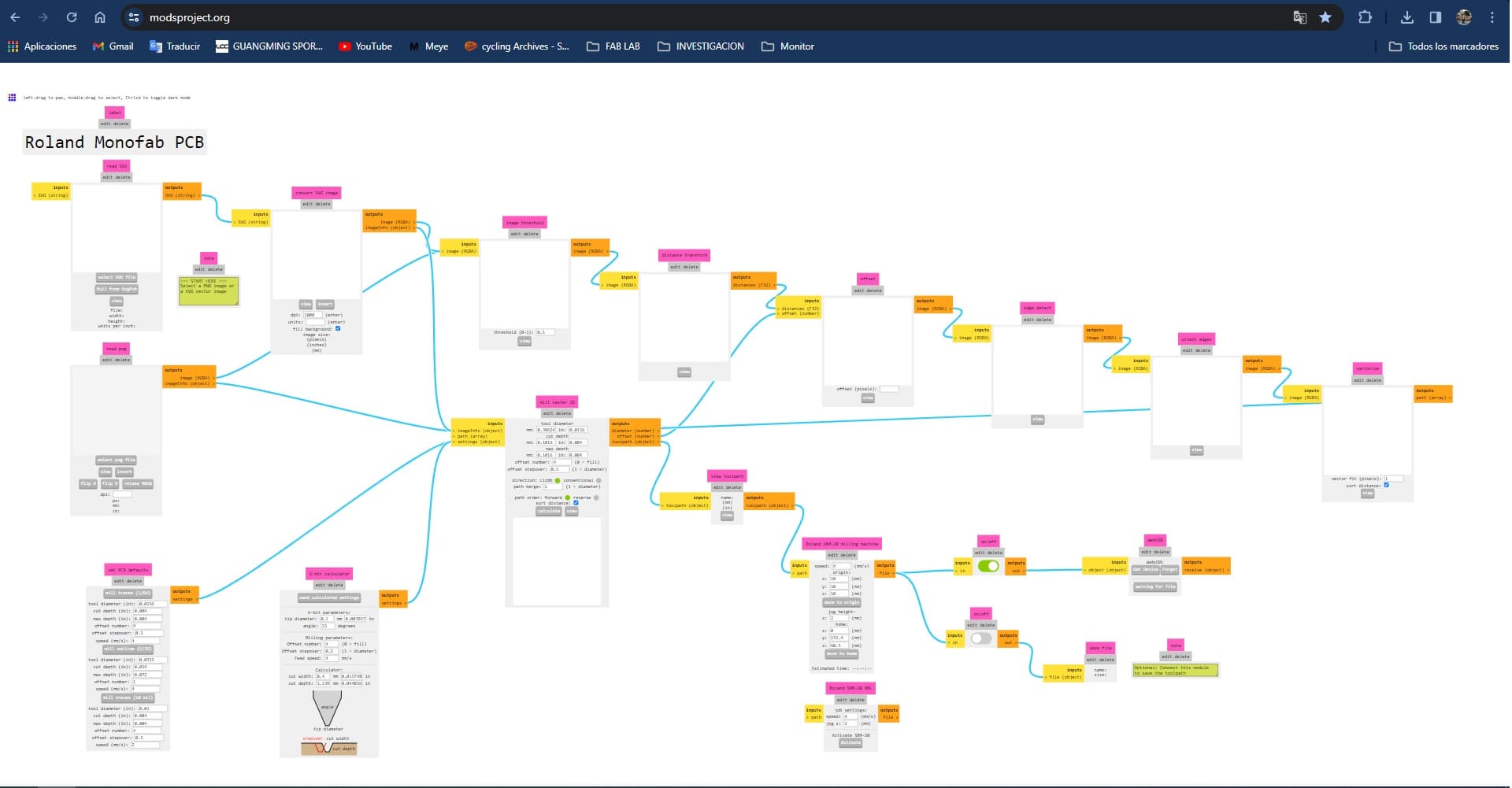
Then we look for the "PNG" option since this time we will work with that type of file, we click on "SELECT PNG FILE" and we look for our file that we want to mill.
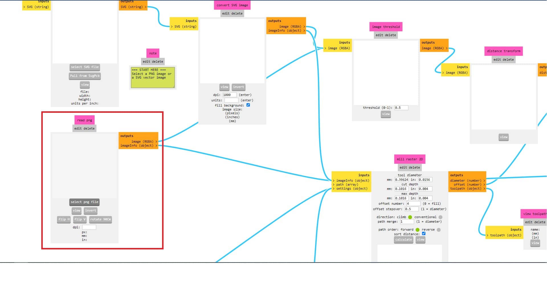
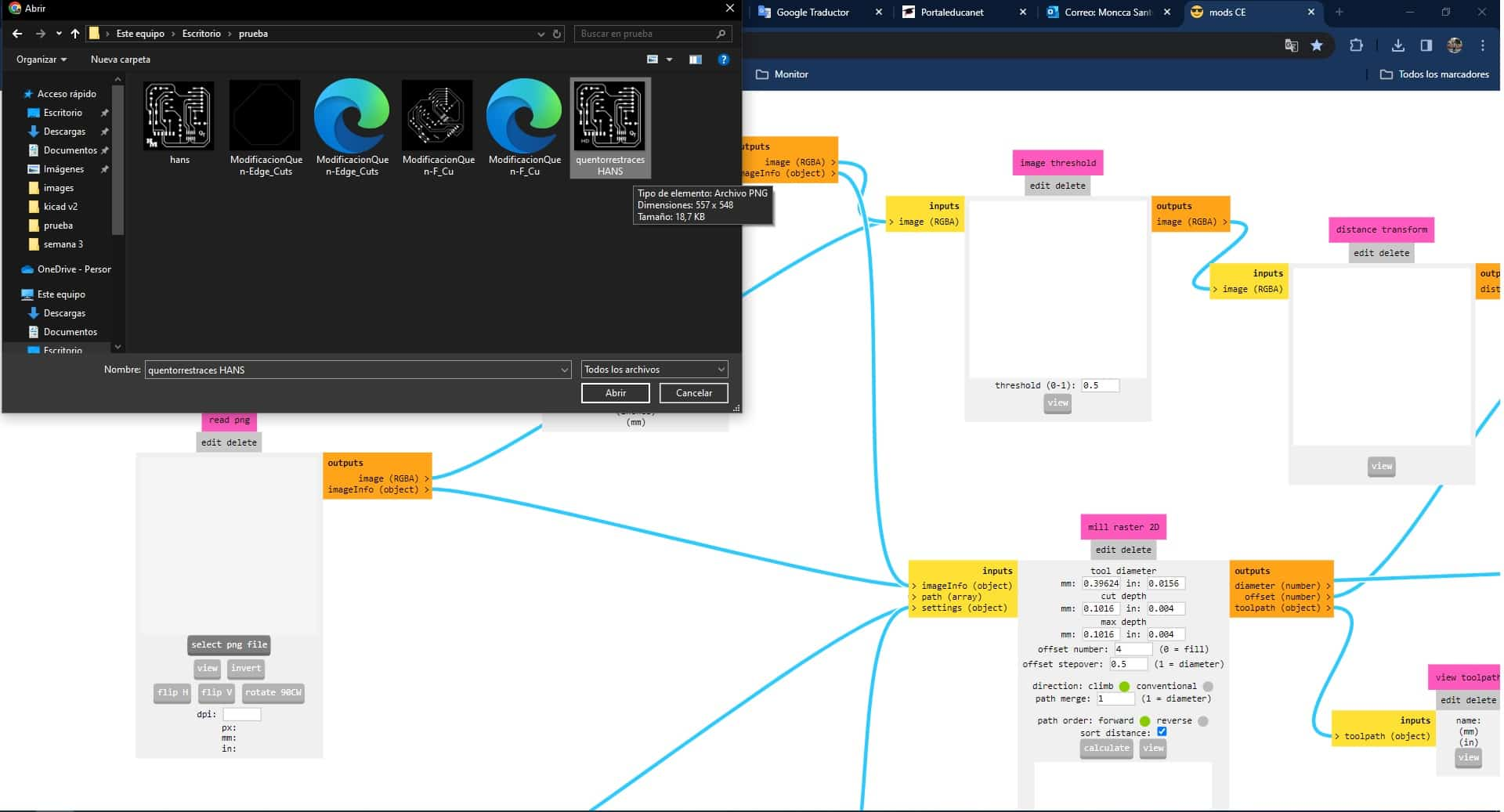
The PNG file will load and begin displaying graphics that are important for milling. Then we look for the "SET PCB DEFAULTS" option where for milling we will choose the "MILL TRACES 1/64" option and when we are going to make a cut we have to choose the "MILL OUTLINE 1/32" . In this case we will choose the first option.
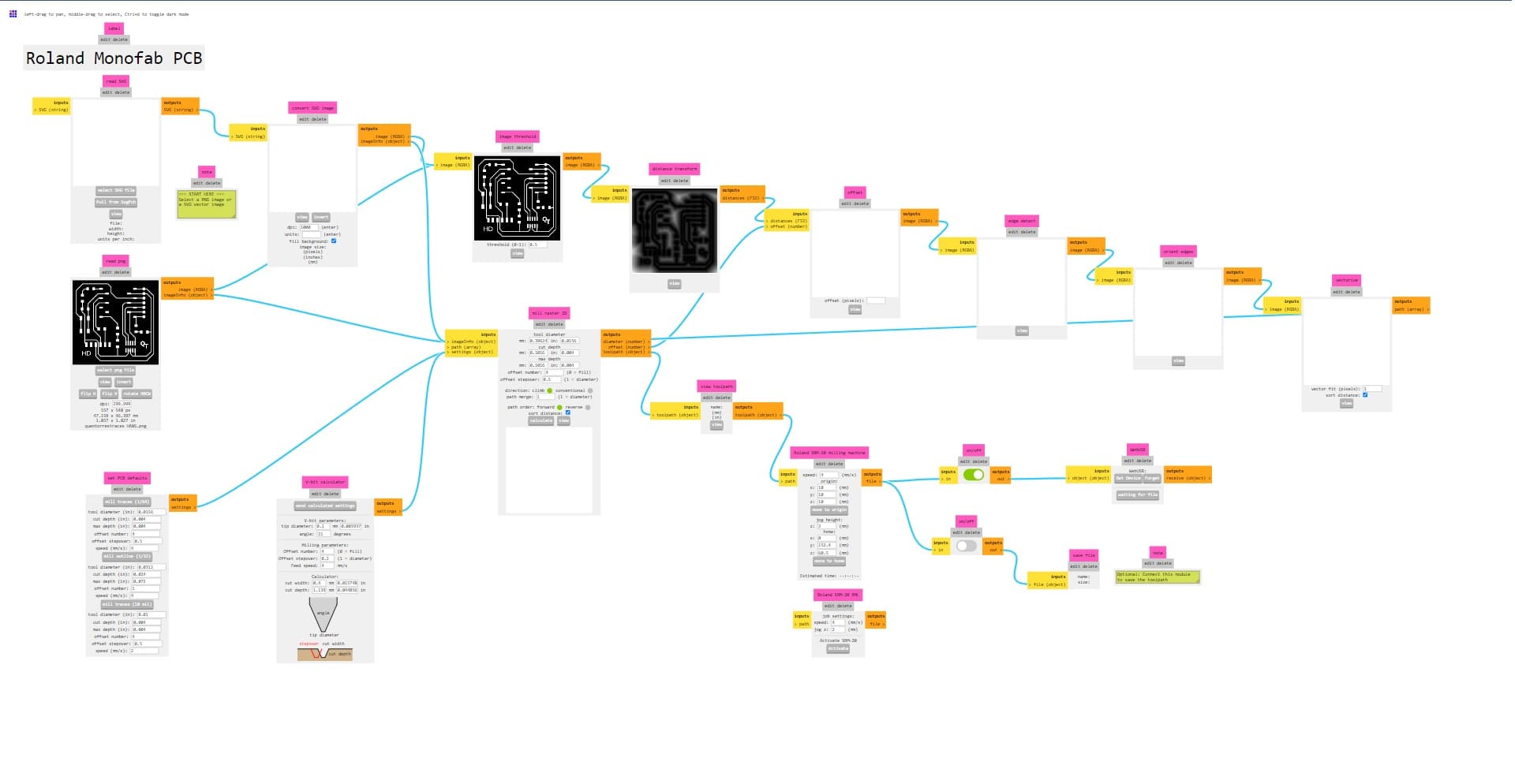
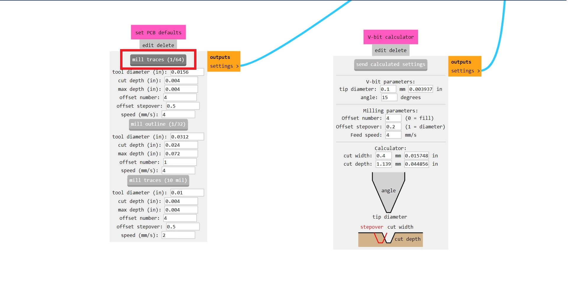
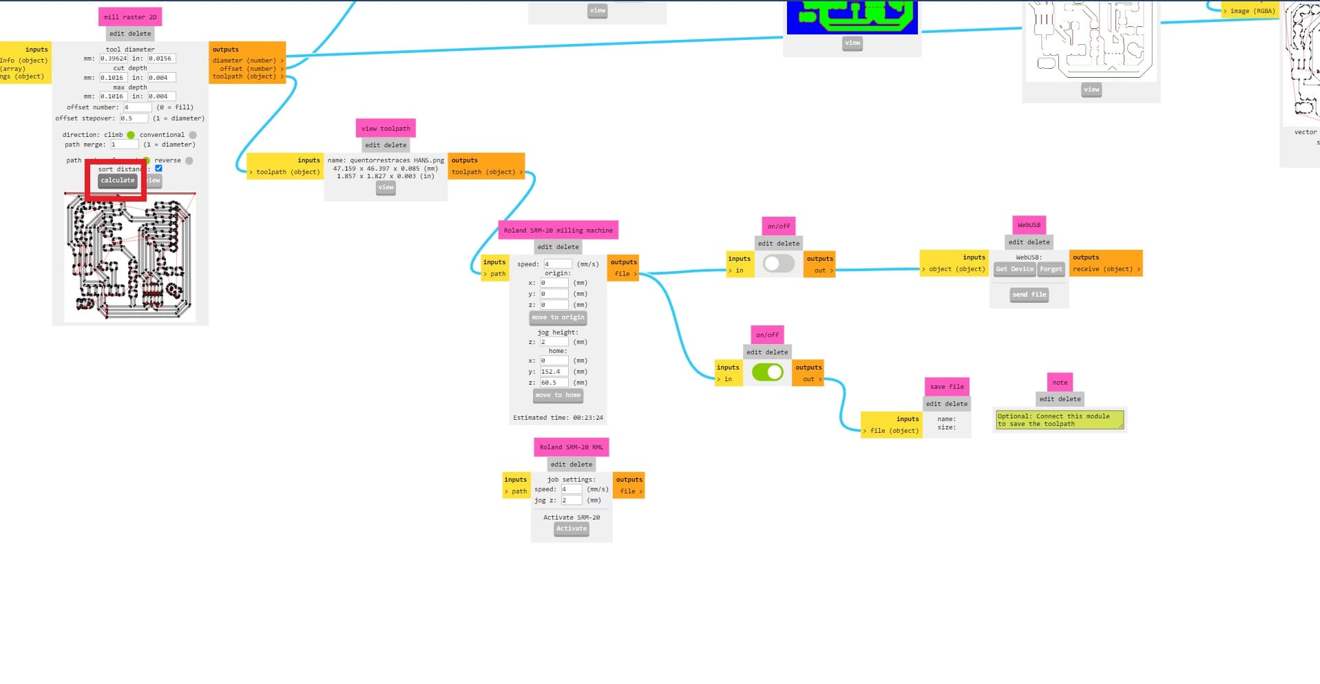
Then we go to the "MILL RASTER 2D" box where we will see the default configuration that the website has when we are going to do the milling with the 1/64 drill bit, however this changes when we choose another drill bit and we have to take these important data into account . Reviewing this we can click on the "CALCULATE" button so that the page can analyze and calculate the cut with the chosen characteristics.
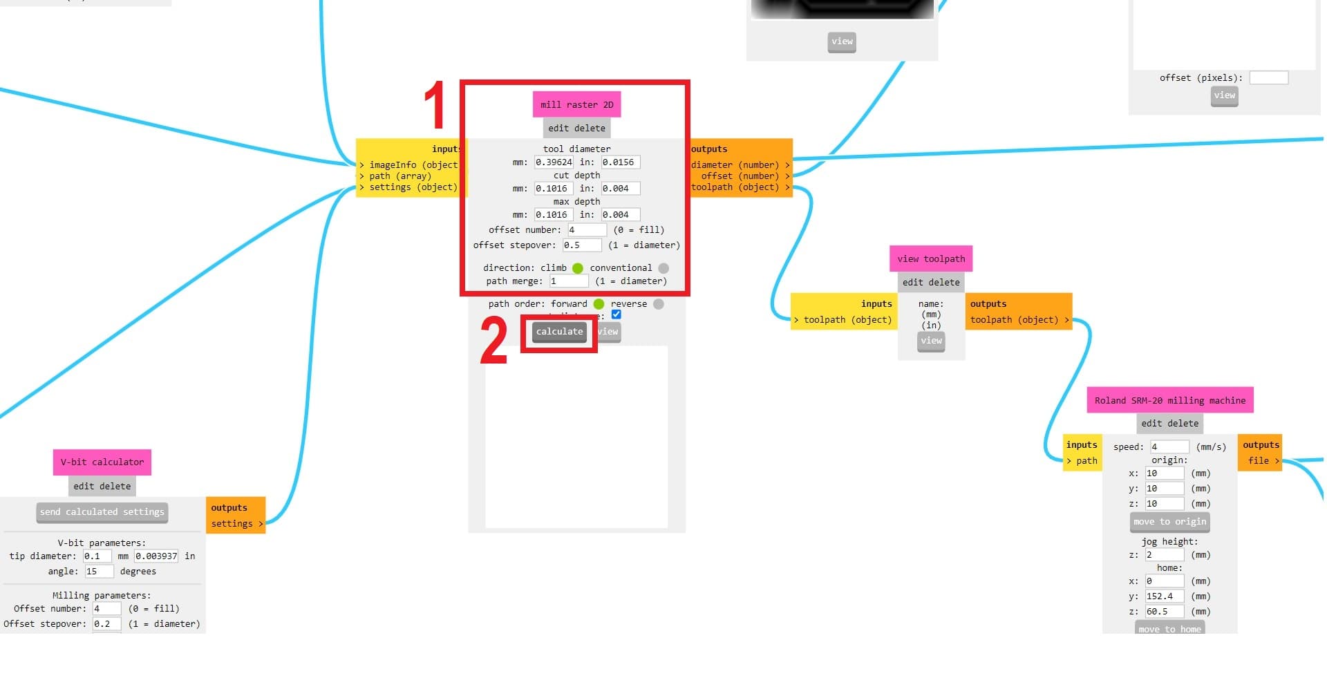
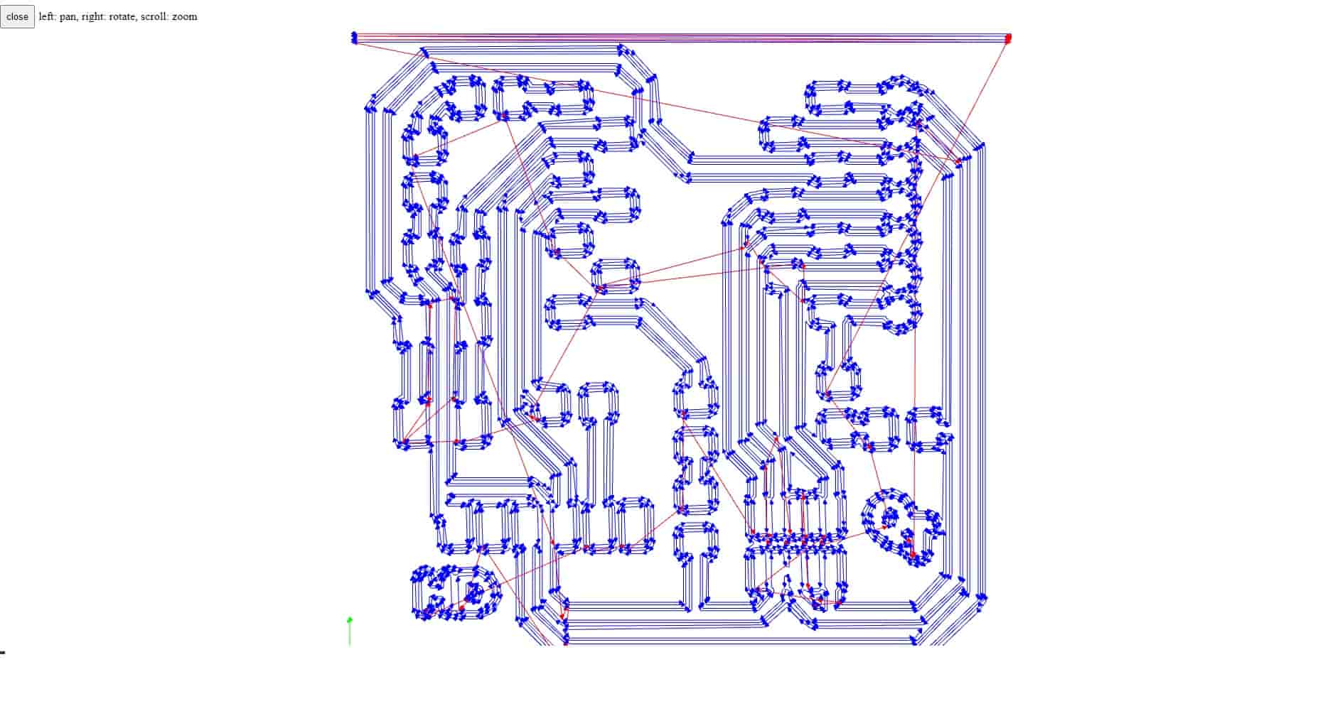
Certain images will be generated that the website needs to analyze our PCB design and a new tab will be generated in the browser with the simulation graph that the drill bit will have to achieve the work we want to achieve in this case of the QUENTORRES.
After checking if all the TRACES are good without having some errors, we go to the "ROLAND SRM-20 MILLING MACHINE" box where we will have to change the X, Y and Z axes in 0.0 so that the machine can cut from our calibration and we have no errors.
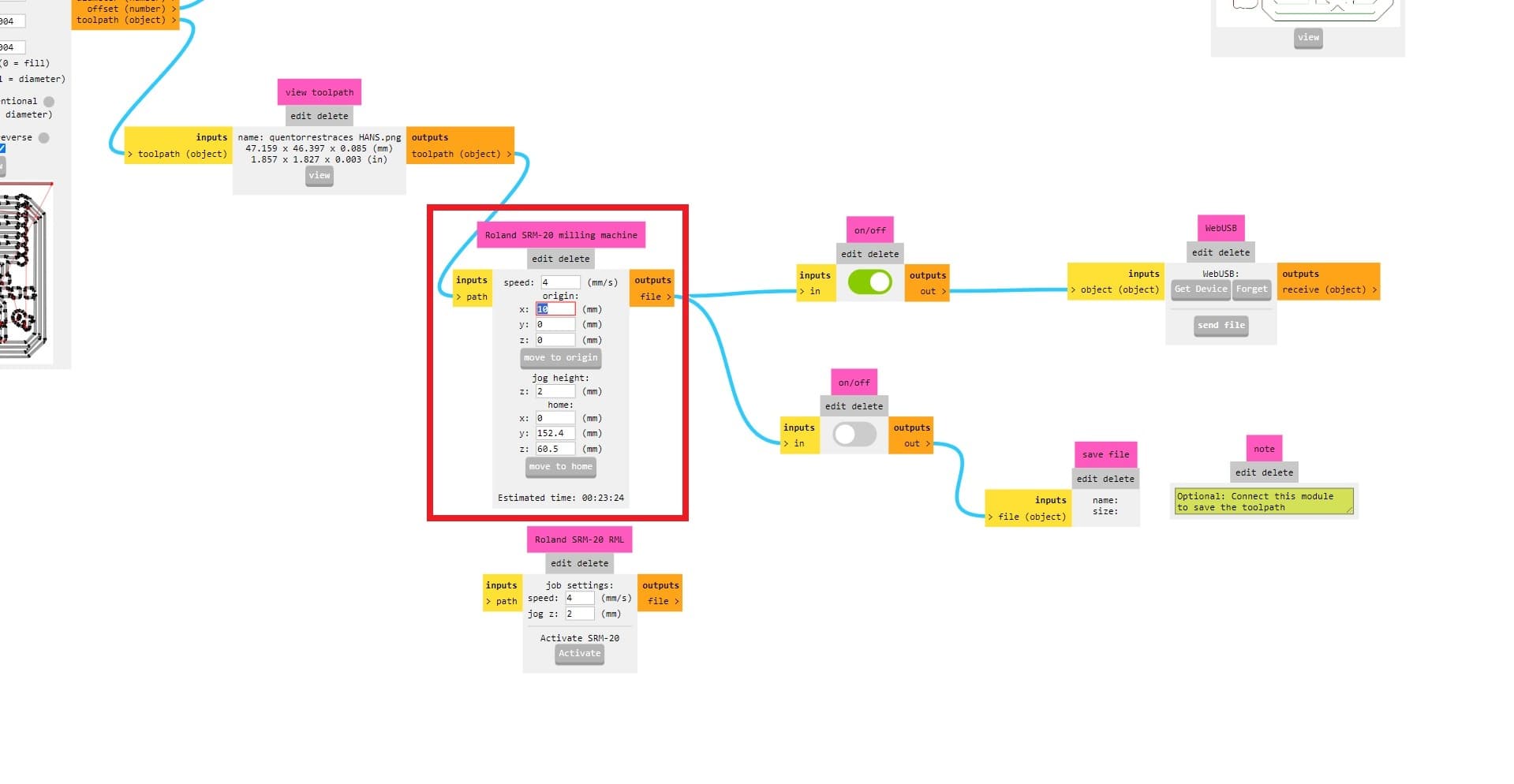
To obtain our file and be able to mill, we have to eliminate the connection from the ROLAND SRM-20 MILLING MACHINE box to ON/OFF of WEBUSB and activate the ON/OFF of SAVE FILE to obtain the downloadable file that we will open with the program. the MONOFAB
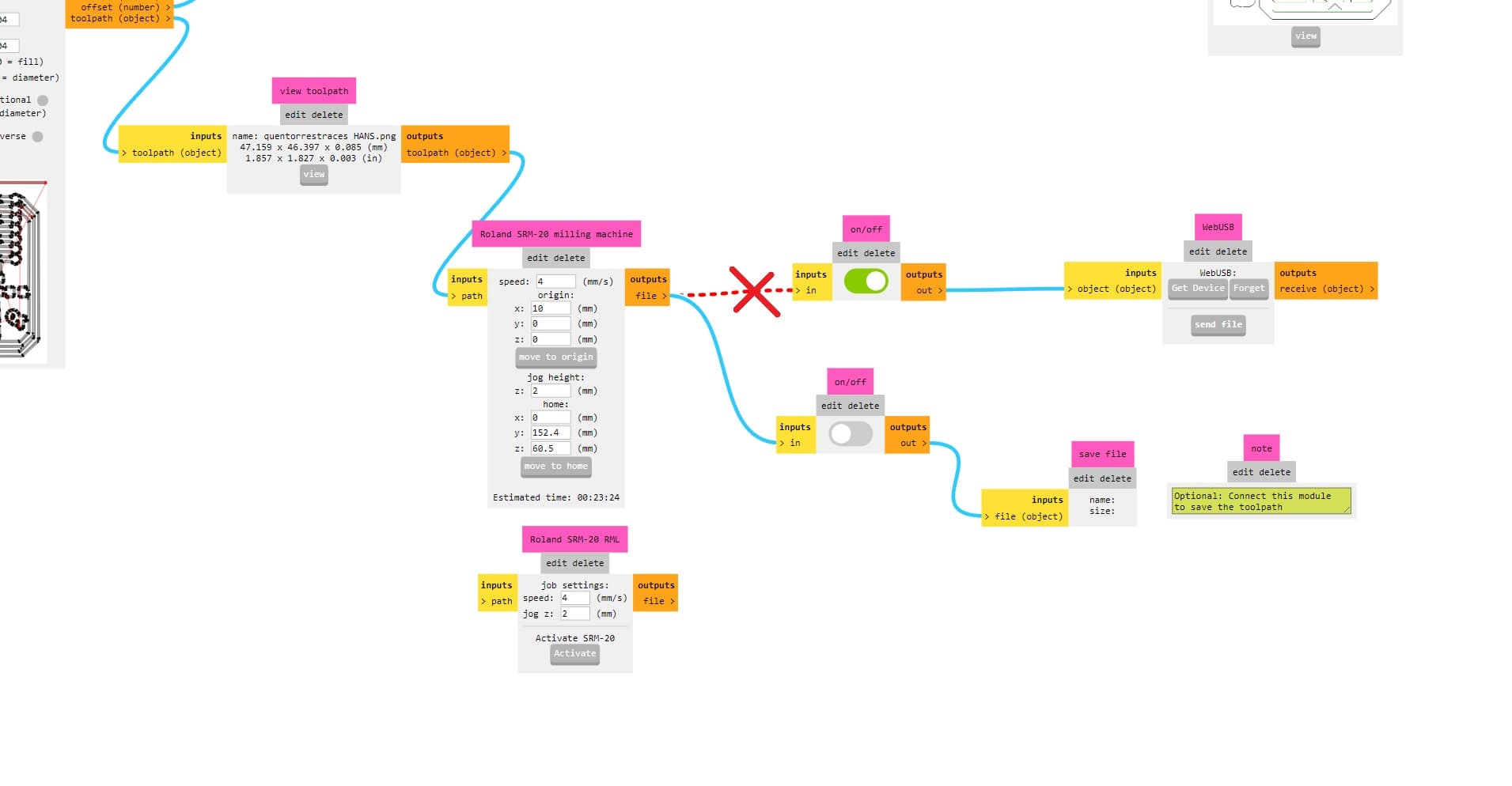
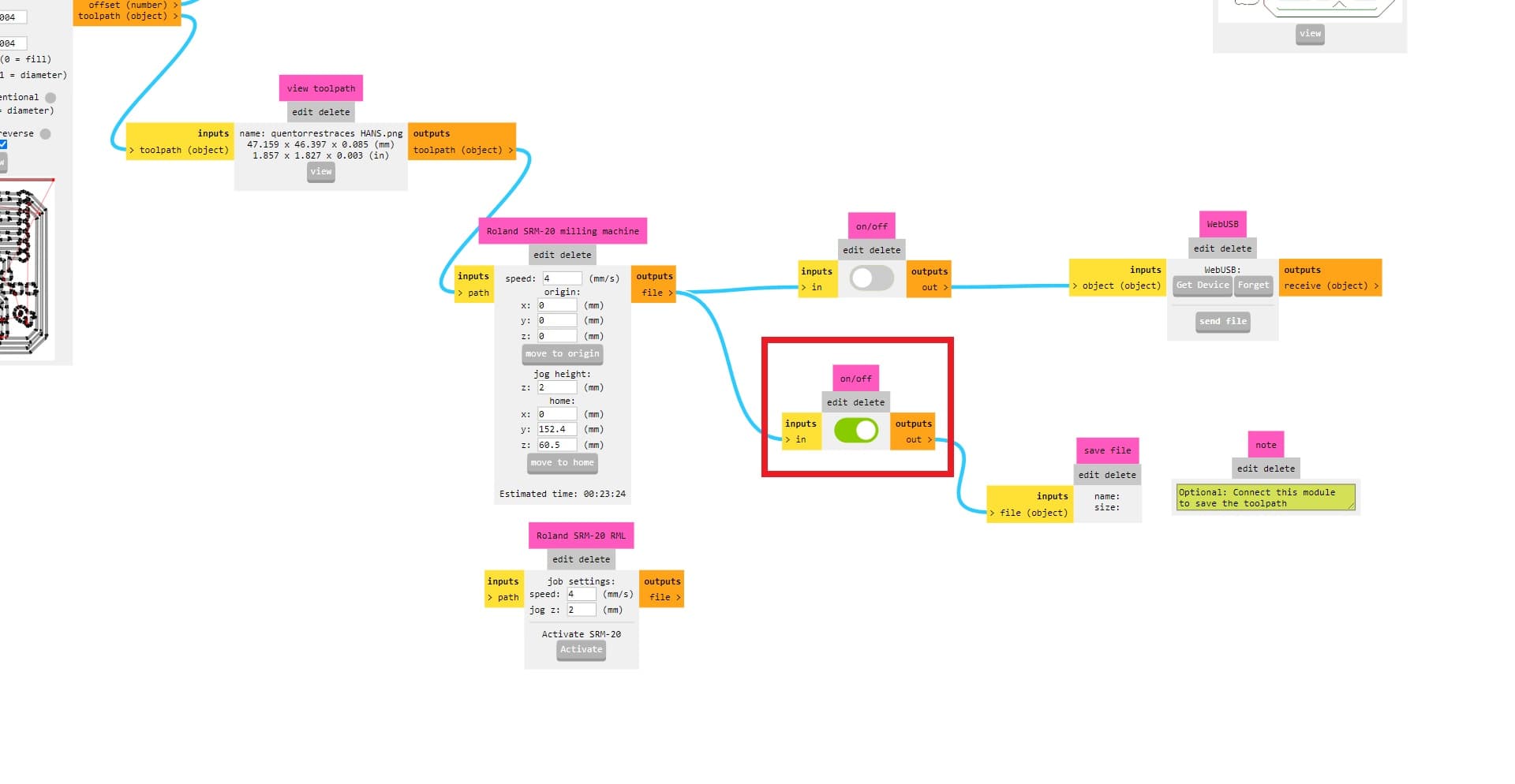
Finally, we click the "CALCULATE" button again and now we will obtain the milling file that we will open with the MONOFAB program.
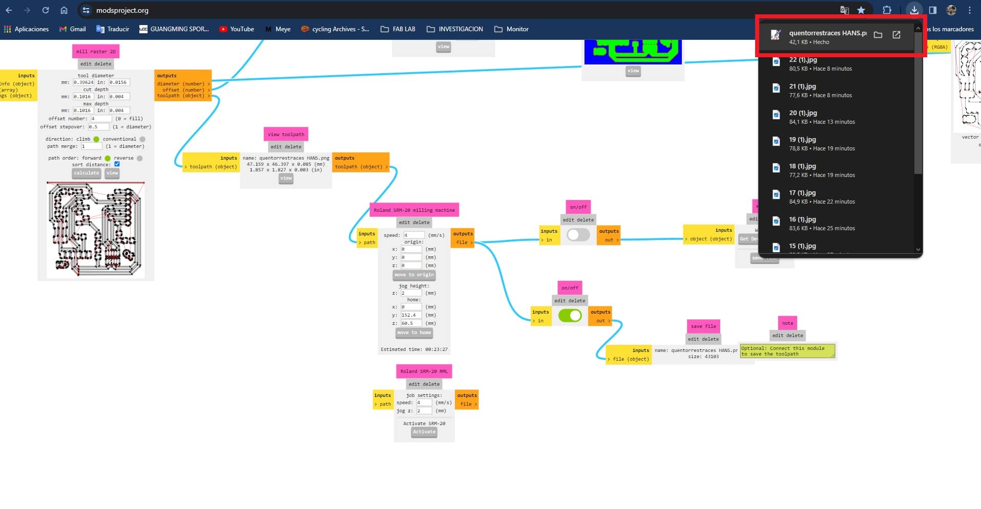
Then we open the MONOFAB software and click on CUT to be able to cut the file that we downloaded previously. We click on DELETTE ALL and search for the file and finally we click on OUTPUT and the machine will only start doing the work.
Here I show some photos and videos of how the machine started working based on the following methodology using MODS.
SOLDERING
To start soldering we had a little advice from our teacher Roberto, where he explained everything about the components, soldering, types of boards and etc. It was very important to understand many things and especially to start soldering the components.
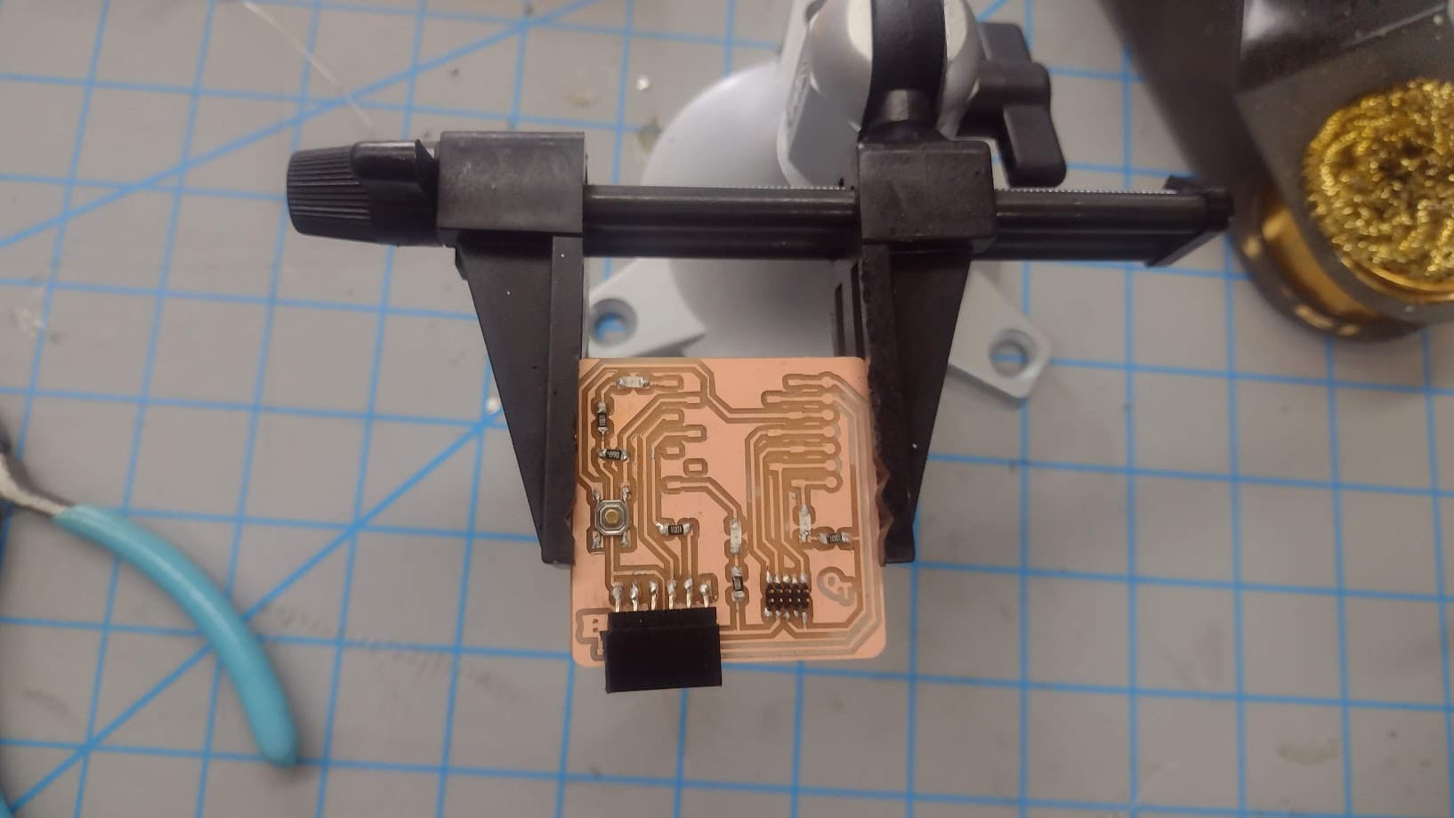
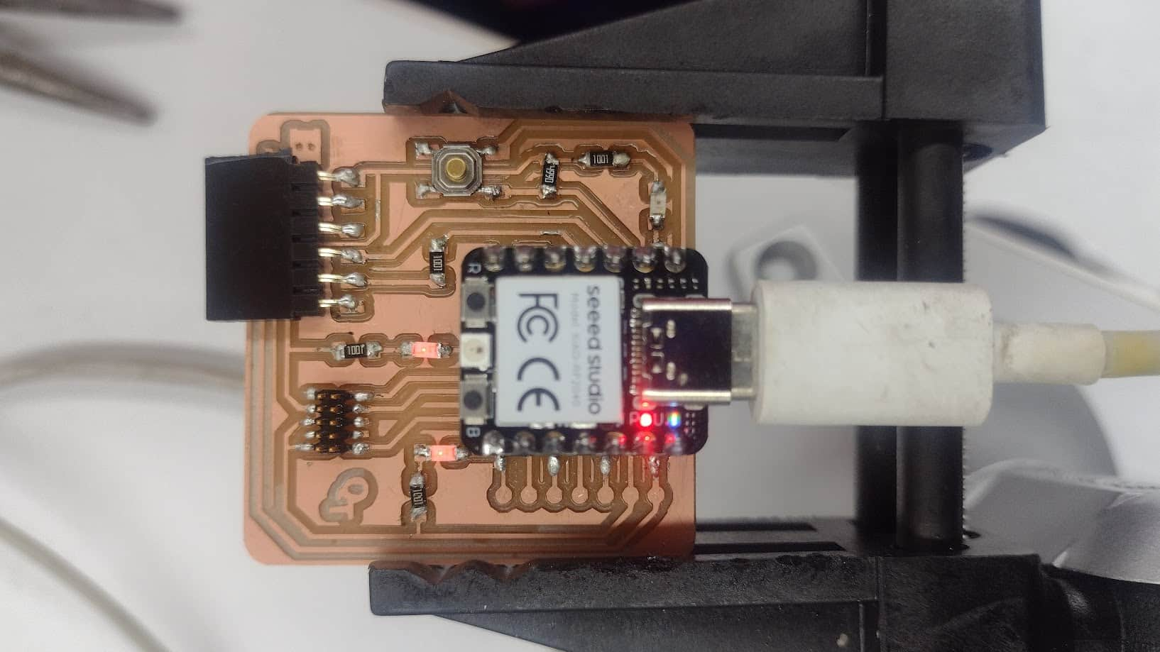
After obtaining the microcontroller board we proceed to solder all the parts it needs for its operation. We have to practice before doing it on the board since we can miss or ruin the circuit routes.
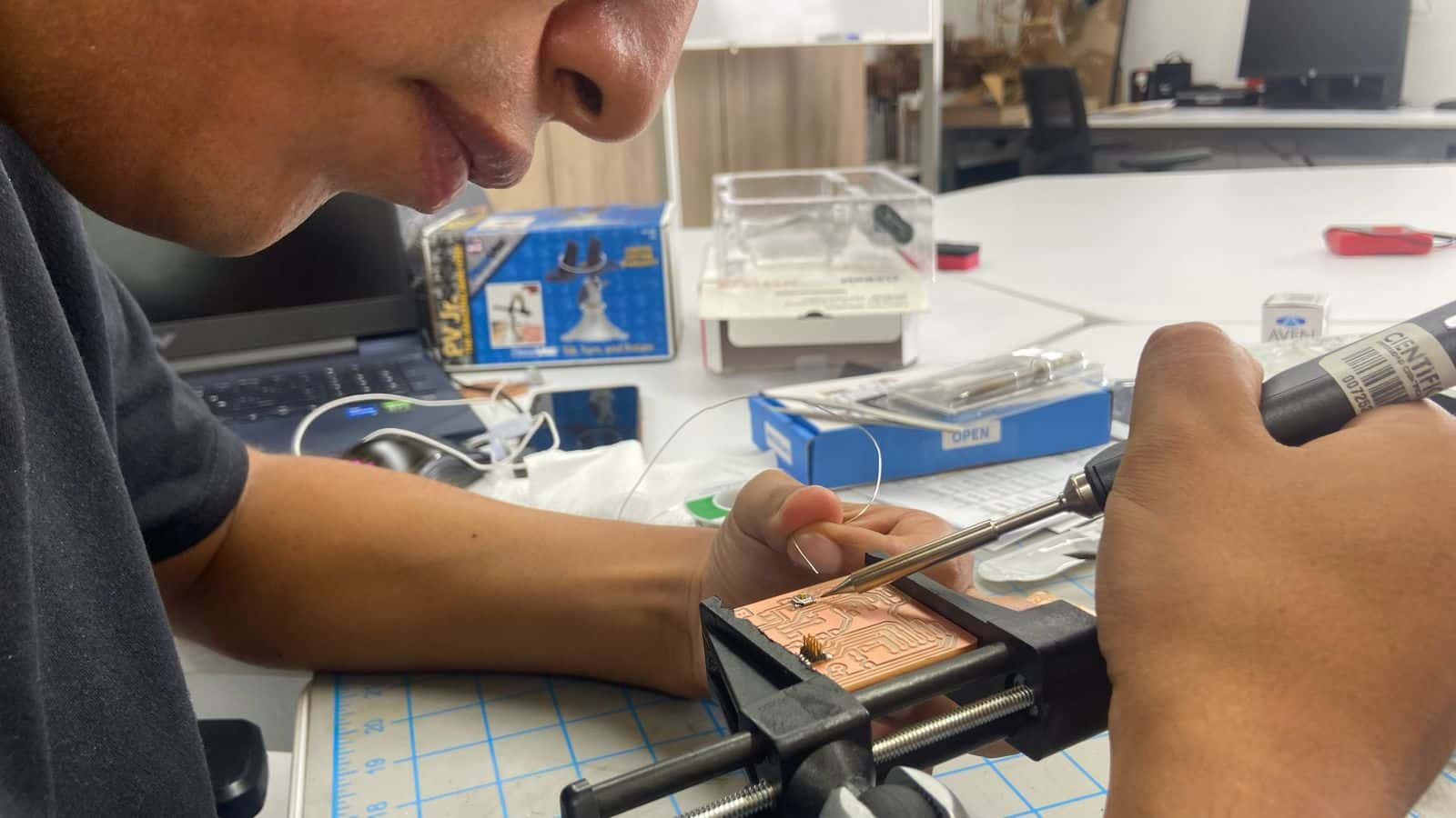
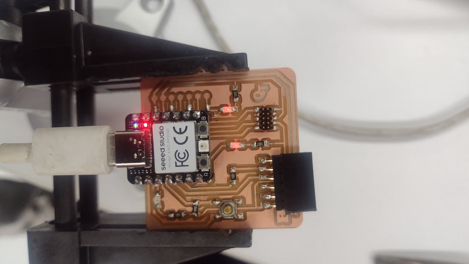
In my case I started to solder the most complicated and small components first since they take time and having other components can affect or burn them. It is better to have more work space and make smaller components in the end. Here is a gallery of the progress until the plate is fully welded.
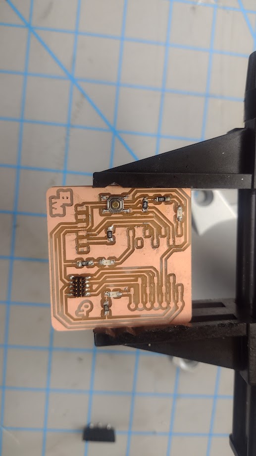
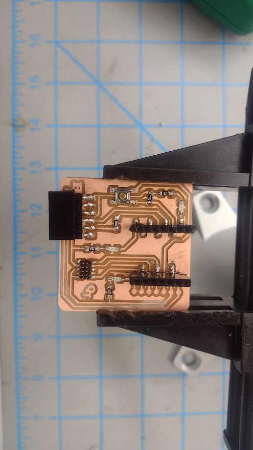
Finally, we locate the XIAO which is one of the main components and we already have the microcontroller ready, now we will move on to programming it.
PROGRAMMING
For programming, we have to go to the QUENTORRES link, attached in the link part at the bottom of this week, where we will see the steps and follow it to achieve the configuration.
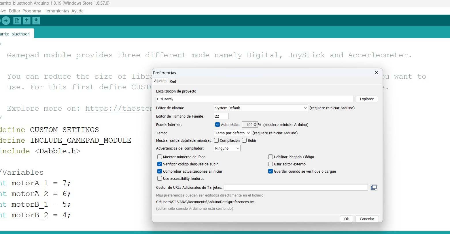
The first step is to open files, then preference and add the URL provided by the QUENTORRES page to add it to the XIAO.
For link 1 just copy the link found in the "installation" part
For link 2 we only need to copy the HTML link
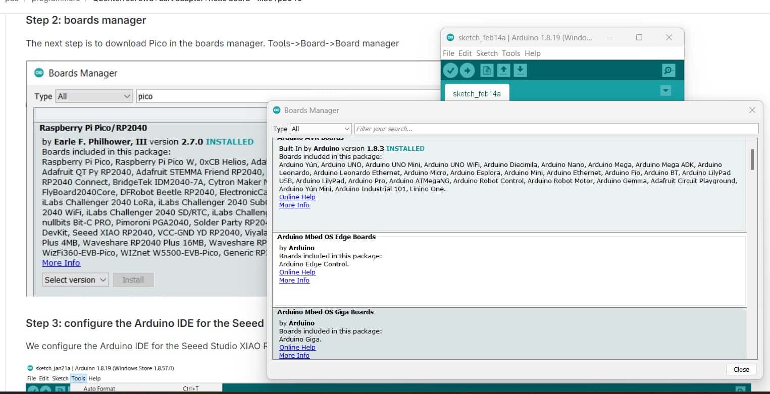
The next step is to download the Pico in the board manager that we find in Tools, we go to Board and finally we locate the Board Manager
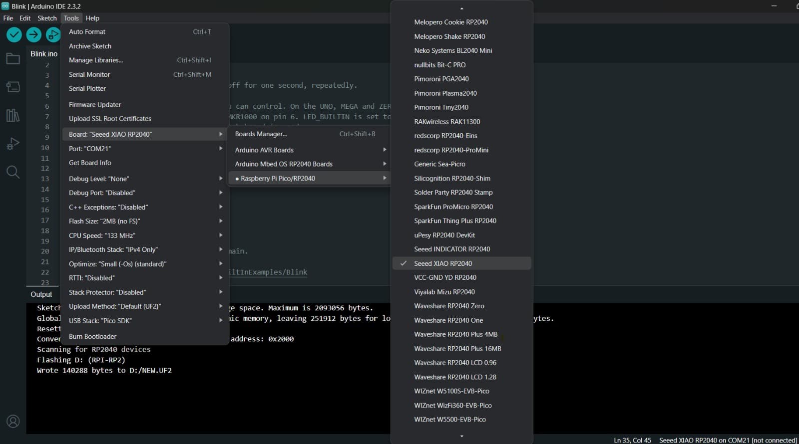
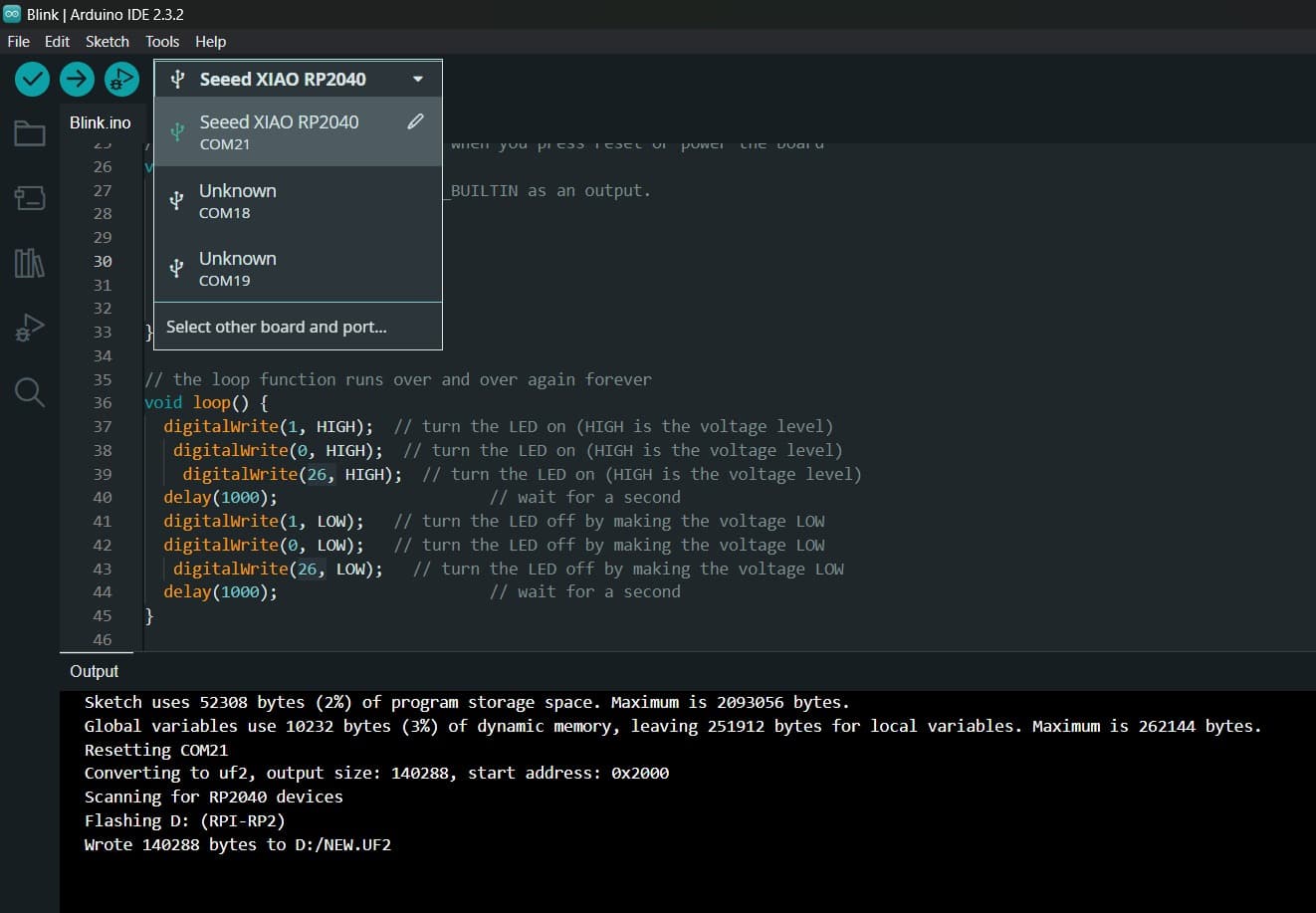
Then we configure the Arduino IDE for the Seeed Studio XIAO RP2040, which will appear in all the options that ARDUINO offers us.
Finally we can test it and we will see that the XIAO will appear as connected, which tells us that everything is fine and that the microcontroller works well.
EXTRACREDIT: PERSONALIZE THE BOARD
DESIGN THE BOARD
In order to customize our board, we have to obtain all the information about the microcontroller that we obtain from the QUENTORRES link so that we can have its operation, components and how it works. We can download it in ZIP format to obtain all that information.
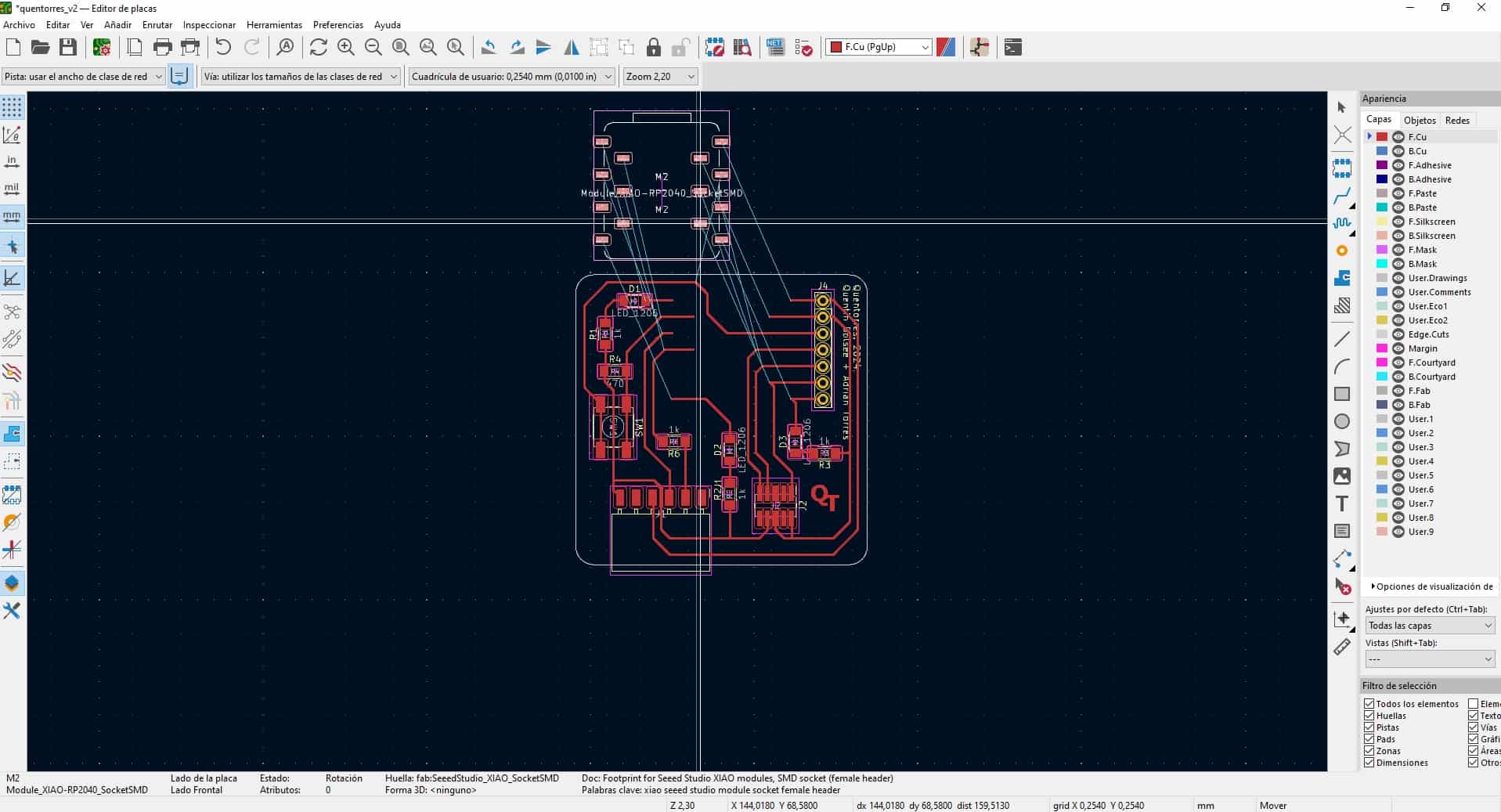
In my case, I only want to change the design and shape of the current board. Since we can modify its operation and components, but because I don't know much about it, I prefer to modify the form and that is why we open KICAD and open the "BOARD EDITOR" file from the folder that we downloaded.
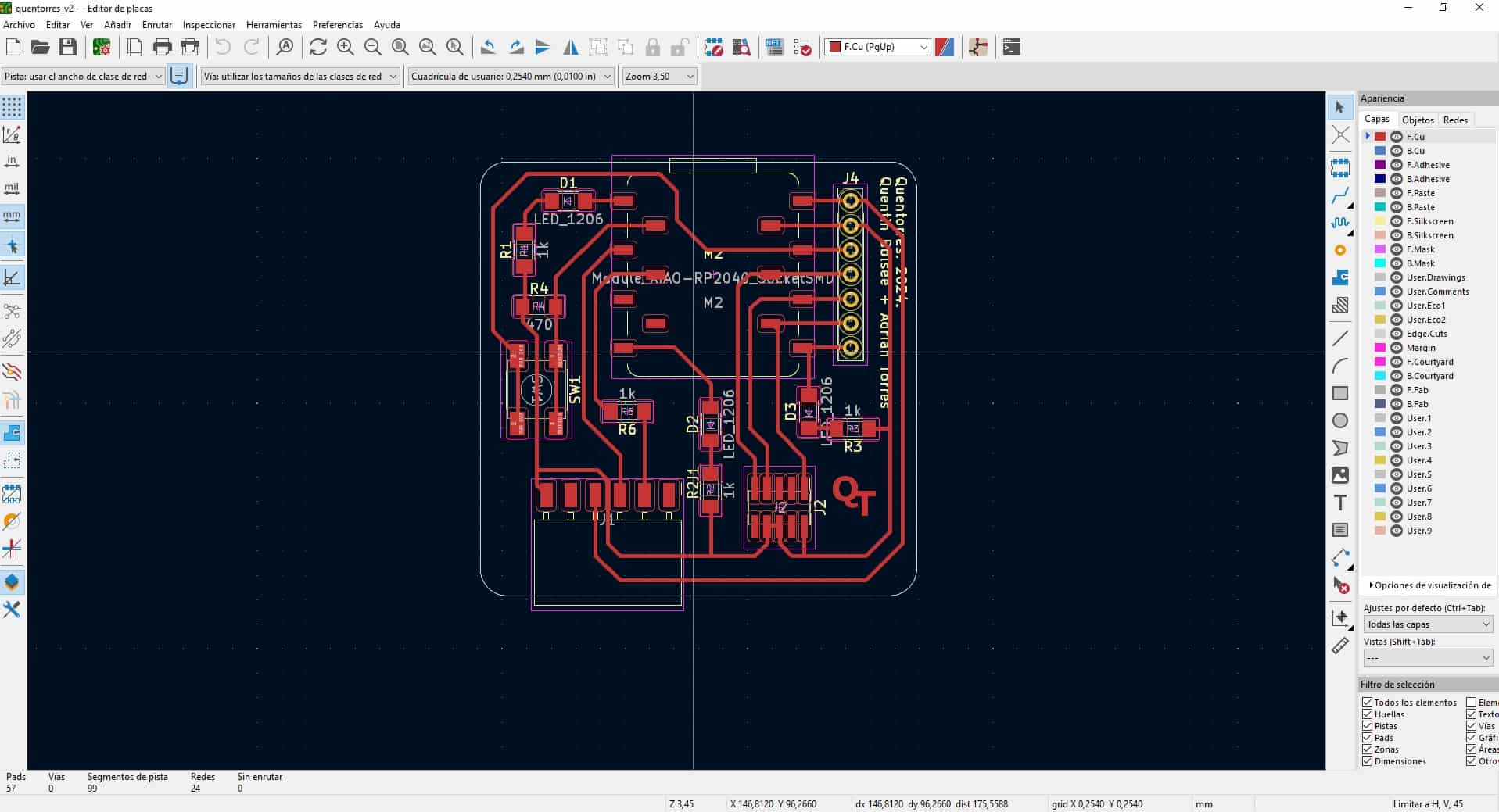
From here we can modify the shape without affecting the function of the components and move it to different shapes since the schematic file of the circuit is maintained and we can make different designs in shape. Here I leave a sample of the change I made to the board in the KICAD software.
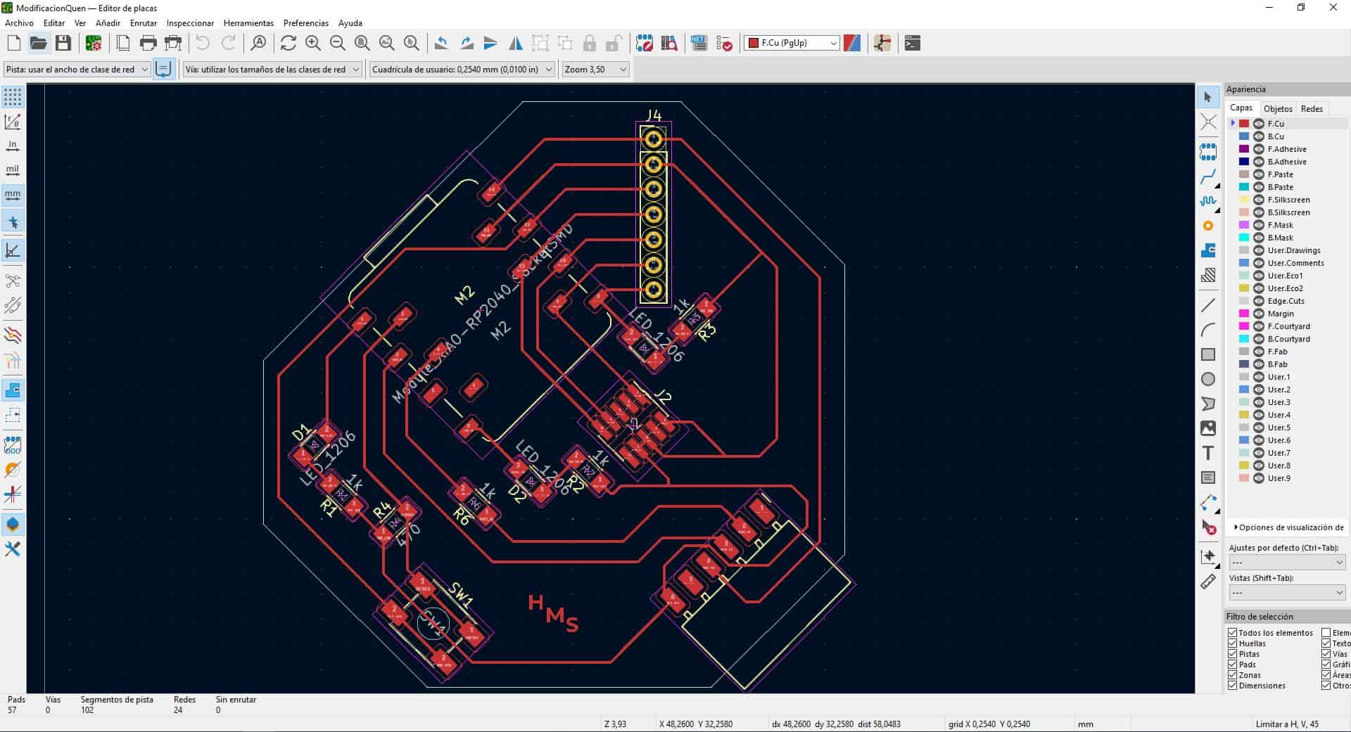
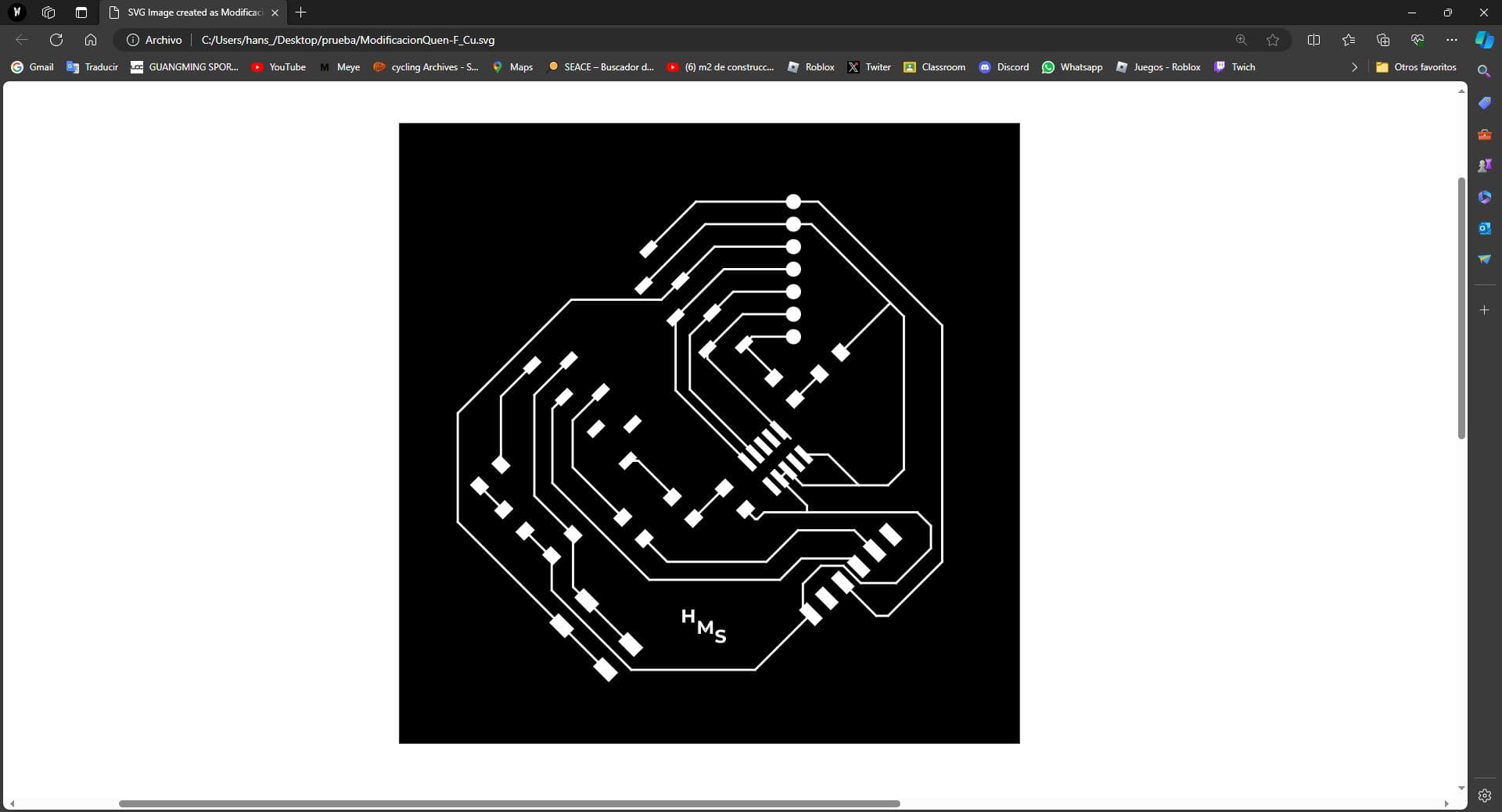
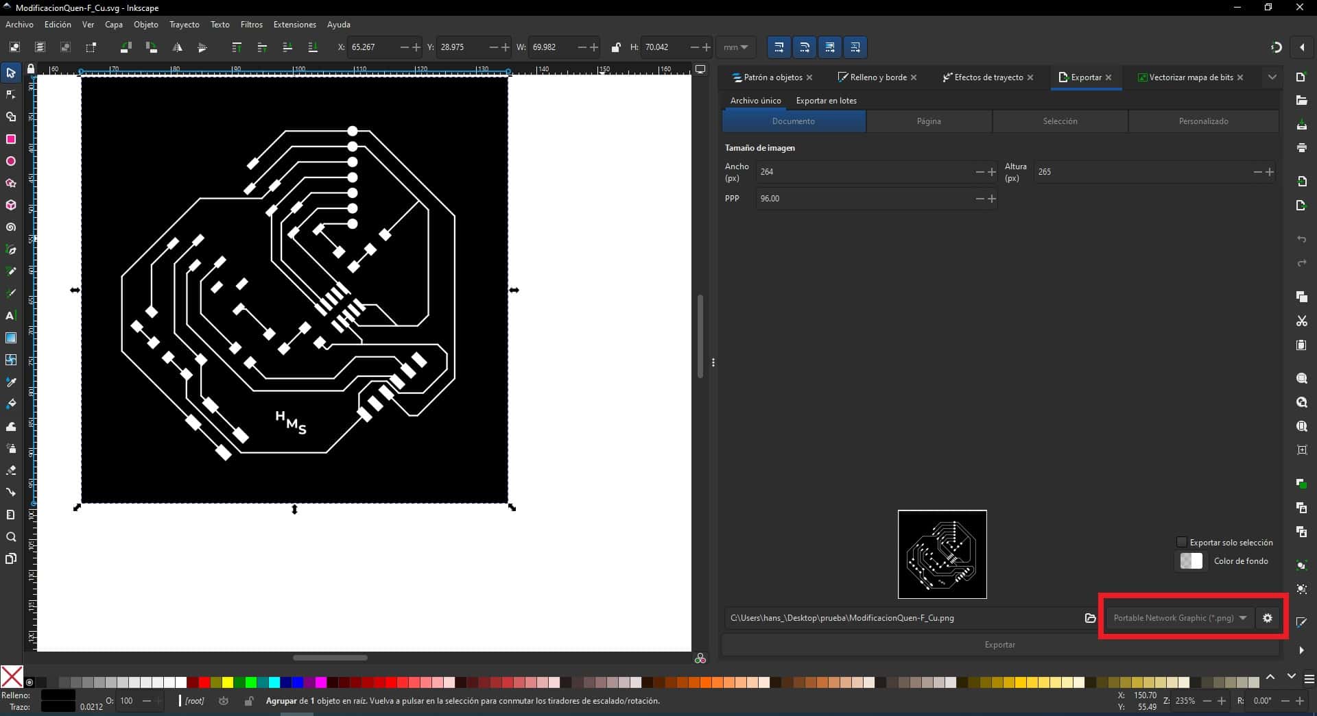
After designing the new shape of the board we move on to export it in SVG, here the program will export the board we designed, we can open it in INKSCAPE to be able to convert it into PNG and be able to mill in MODS.
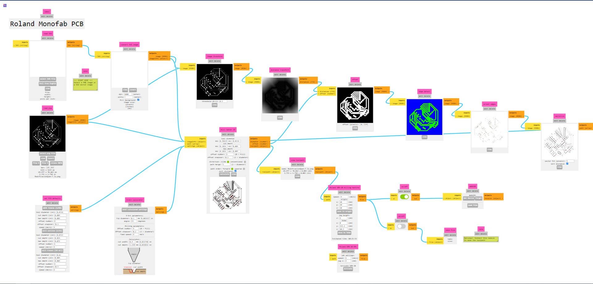
We proceed to cut into the MONOFAB to see if the board is properly designed and to see if the components and tracks can work in the new design.
FILES
Here you can download all the files that I have made for the following assignment: