Results: Electronics Design
As an architect, I have programmed little until now. During week 6, I felt very motivated after programming the hygrometer on the Quentorres PCB. Therefore, I felt that this week could be challenging, but I would make it.
And I did it! I programmed an hygrometer with XIAO RP2040 microcontroller in my final project PCB so it shows in the serial monitor in Arduino IDE the percentage of humidity measured. I used this code in Arduino IDE:
// constants
const int hygrometer = A2;  // hygrometer sensor analog pin output at pin A2 of XIAO RP2040
// variables
int value;

void setup(){

  Serial.begin(9600);
}

void loop(){
  // when the plant is watered well the sensor will read a value 380∼400, I will keep the 400
  // value but if you want you can change it below.

  value = analogRead(hygrometer);     // read analog value
  value = constrain(value,400,1023);  // keep the ranges
  value = map(value,400,1023,100,0);  // map value: 400 will be 100 and 1023 will be 0
  Serial.print("Soil humidity: ");
  Serial.print(value);
  Serial.println("%");
  delay(10000);                       // read every 10 seconds
}
Code in Arduino IDE for programming the hygrometer
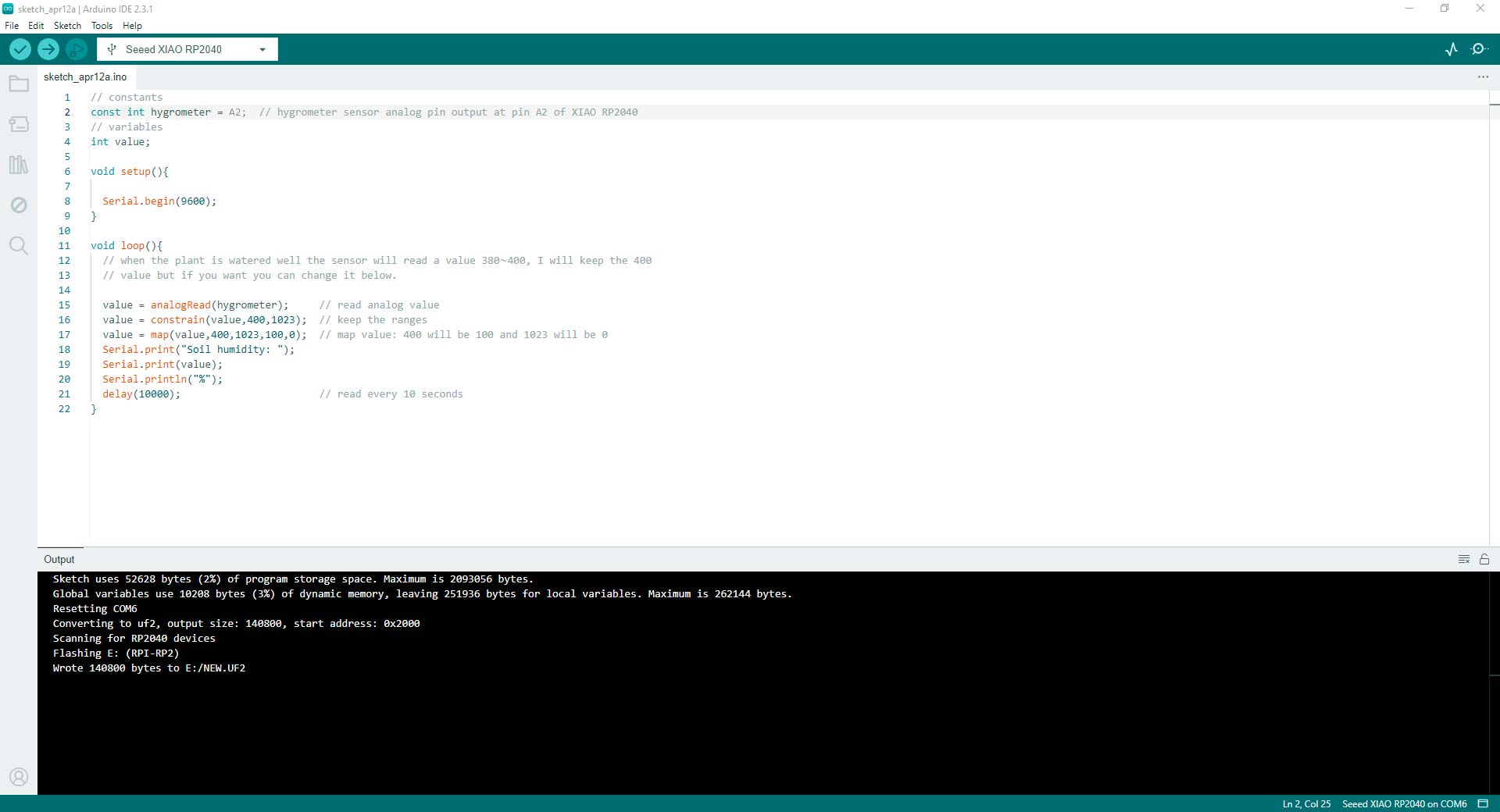
Code of hygrometer well programmed
There was very intense work this week. I still feel that I have a long way to go in the electronics world but I am understanding better the concepts and how to use the components.
Preliminary Concepts
In this week, I learned some technical electronic words.
Glossary
- Ohm's law definition: A fundamental principle stating that the current passing through a conductor between two points is directly proportional to the voltage across the two points.
- Ohm's law formula: V = I * R, where V is voltage, I is current, and R is resistance.
- Electricity: The flow of electric charge.
- Current: The rate of flow of electric charge, measured in amperes (amps).
- Voltage: The difference in electric potential between two points, measured in volts.
- Resistance: The measure of opposition to the flow of electric current, measured in ohms.
- Continuity: The uninterrupted path for electric current flow.
- Power source:A device that provides electrical energy, such as batteries or power supplies.
- Resistors:Passive electronic components that resist the flow of electric current.
- Capacitors (or condensers):Passive components that store electrical energy in an electric field.
- Diodes:Semiconductor devices that allow current to flow in one direction only.
- Pull-up or pull-down resistor:Resistors used in digital circuits to ensure a well-defined voltage level when no other active device is driving the signal.
- Transistor:A semiconductor device used for amplification, switching, or signal modulation.
- Microcontroller:A small computer on a single integrated circuit containing a processor core, memory, and programmable input/output peripherals.
- Integrated circuit (IC):A semiconductor chip consisting of interconnected electronic components such as transistors, resistors, and capacitors.
- Logic gate:A fundamental building block of digital circuits that performs a logical operation on one or more binary inputs and produces a single binary output.
- Logic analyzer:An electronic instrument that captures and displays multiple digital signals.
- Logic level:The voltage range used to represent binary values (e.g., 0 and 1) in digital circuits.
- Development board:A printed circuit board containing the necessary components for experimenting with or developing electronic projects, often including a microcontroller or other integrated circuits.
- Ampere (Amp): The unit of electric current, equivalent to the flow of one coulomb per second.
- Volt: The unit of electromotive force, representing the electrical potential difference between two points.
- Watt: The unit of power, representing the rate of energy transfer or consumption.
Group Assignment: Test Equipment
The group assignment page is here.
What I Learned From Team Work
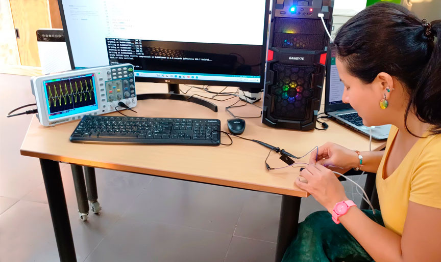
To use the oscilloscope and multimeter -as a team- we went to IEST Simon Bolivar Fab Lab which is located in Bellavista district in Callao, Peru.
Using the Test Equipment
The oscilloscope is a versatile electronic instrument used to visualize and analyze the waveform of electrical signals over time. It displays the amplitude (voltage) of a signal on the vertical axis and time on the horizontal axis, allowing users to observe the shape, frequency, amplitude, and other characteristics of the signal. Oscilloscopes are commonly used in various fields, including electronics, telecommunications, physics, and engineering, for tasks such as troubleshooting circuits, measuring signal integrity, analyzing frequency response, and debugging electronic systems. Modern oscilloscopes often come with advanced features such as digital storage, multiple channels, various trigger options, and built-in signal processing capabilities.
For this task, we used the OWON SmartDS. For learning its usage, we followed this tutorial and the user manual.
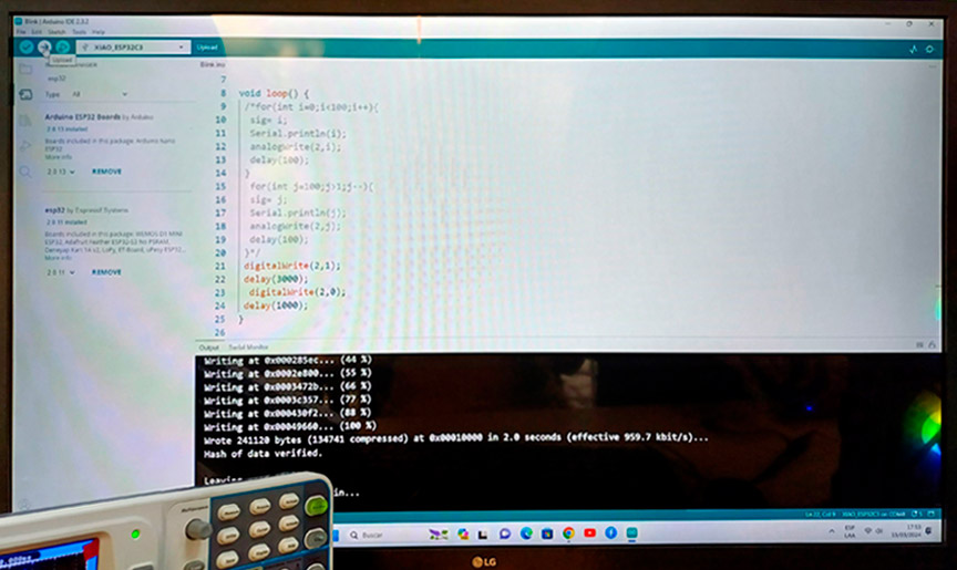
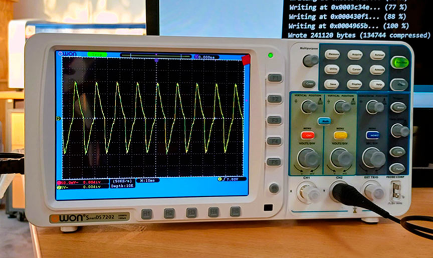
Triangle waves from blinking programmation in XIAO ESP32-C3
During the process of measuring an LED in a circuit with a Xiao ESP32-C3 board, I encountered two different situations. Initially, when using an oscilloscope, I obtained a triangular wave instead of the expected square wave. My instructor's feedback suggested that the oscilloscope probe was incorrectly configured for AC measurements instead of DC. Without further access to the oscilloscope, I turned to a simulation in Tinkercad, which correctly displayed a square wave. This exercise taught me the importance of accurate oscilloscope probe configuration and the usefulness of simulation tools for validating results when physical equipment is unavailable.
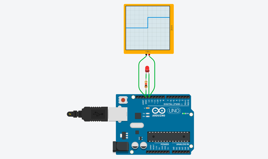
Rectangular waves from blinking programmation in Tinkercad oscilloscope simulator
The multimeter is a handheld electronic instrument used to measure multiple electrical quantities such as voltage, current, and resistance. It typically consists of a display screen, selection dial, and probes or test leads. Multimeters can be used in various applications, including electronics, automotive diagnostics, electrical engineering, and household tasks. They are versatile tools capable of performing several functions: voltage, current and resistance measurement. Some multimeters also offer additional features such as continuity testing, diode testing, capacitance measurement, and transistor testing. They are essential tools for both professionals and hobbyists in the field of electronics and electrical engineering, providing valuable information for circuit analysis, troubleshooting, and maintenance.
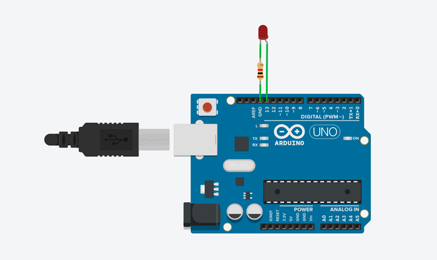
In my case, I own the UT33B+. For learning its usage, I followed this tutorial and the user manual. I used this code in Arduino IDE:
const int ledPin = D7; // Pin D7 on Xiao rp2040

// the setup function runs once when you press reset or power the board
void setup() {
// initialize digital pin LED_BUILTIN as an output
  pinMode(ledPin, OUTPUT);
}

// the loop function runs over and over again forever
void loop() {
  digitalWrite(ledPin, HIGH);       // turn the LED on (HIGH is the voltage level)
  delay(1000);                      // wait for a second
  digitalWrite(ledPin, LOW);        // turn the LED off by making the voltage LOW
  delay(1000);                      // wait for a second
}
Code in Arduino IDE for programming LED in Quentorres
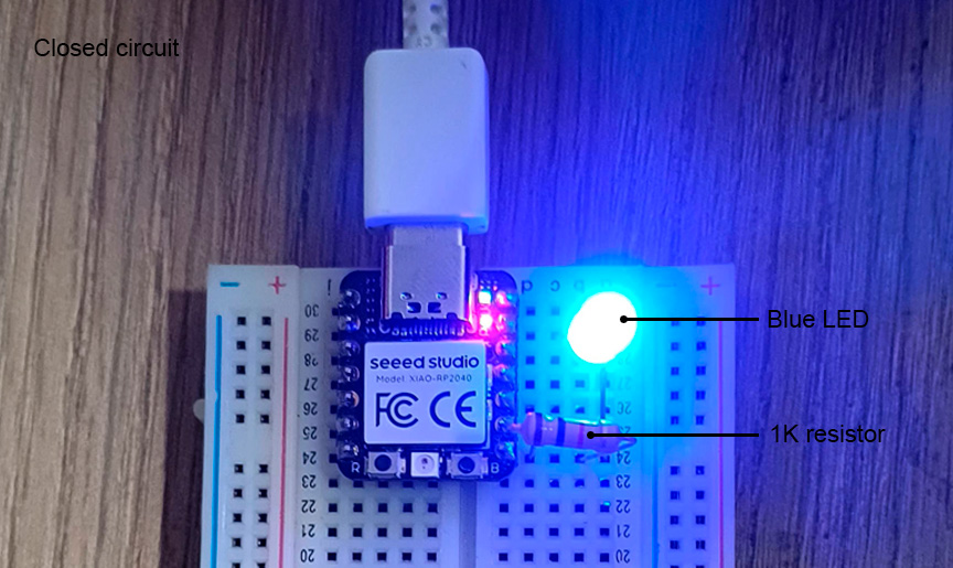
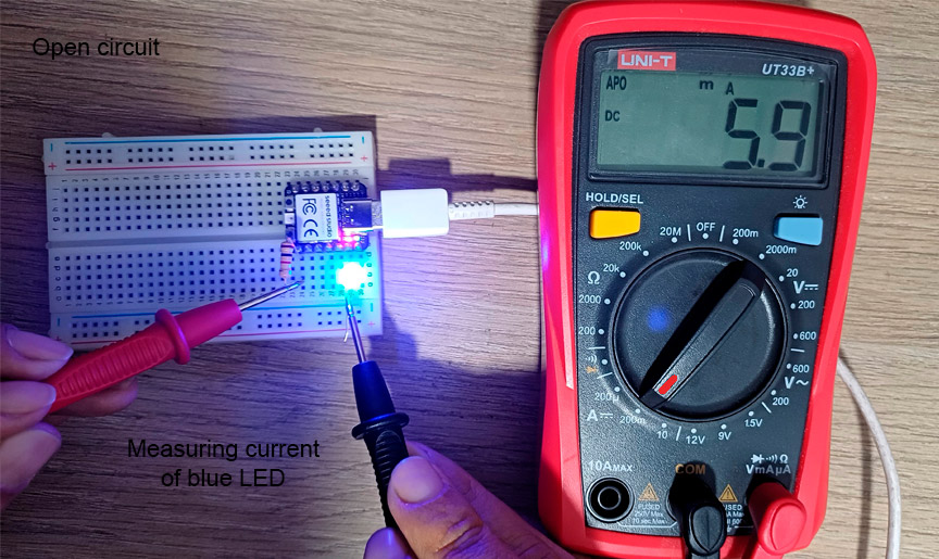
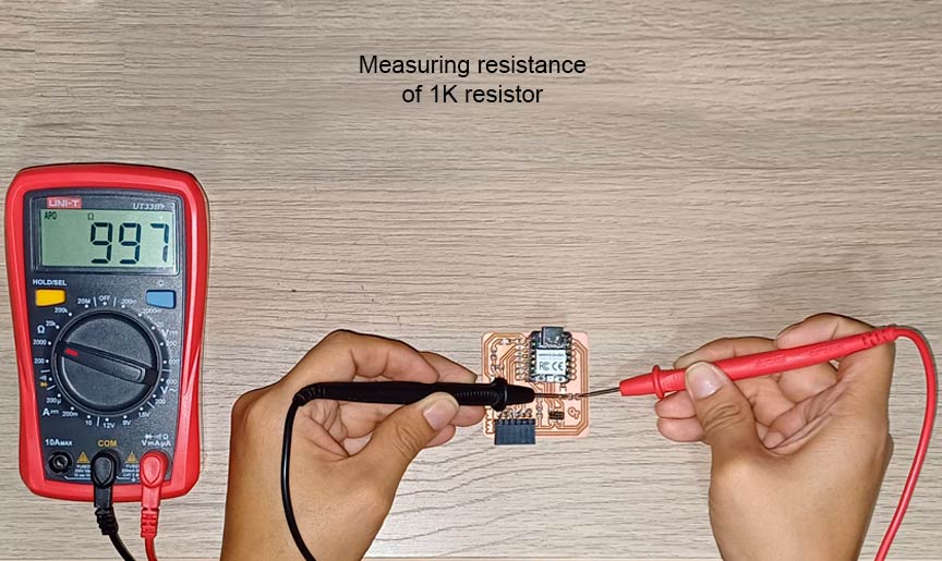
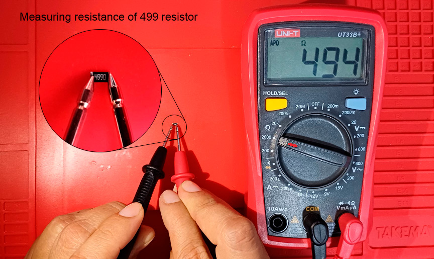
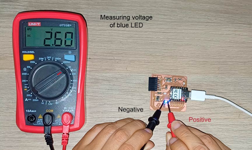
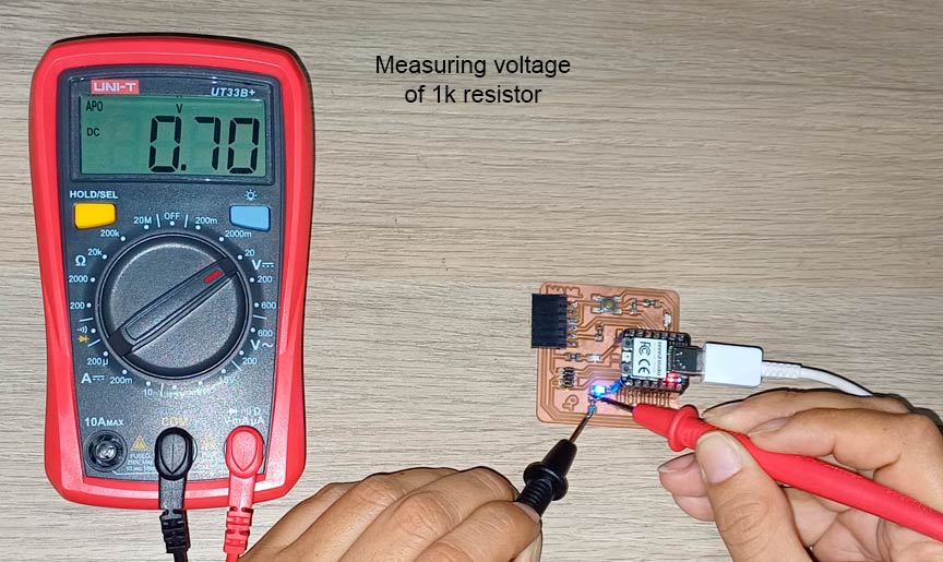
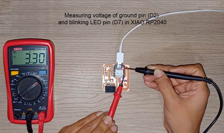
Measuring current, resistance and voltage with the multimeter
Conclusions:
- The oscilloscope serves as an indispensable tool in electronics, offering real-time visualization and analysis of electrical signals. By displaying voltage waveforms over time, it enables to assess signal characteristics, diagnose circuit issues, verify performance, and debug electronic systems with precision.
- The multimeter stands as an essential tool for electrical measurements. By enabling users to measure voltage, current, resistance, and other electrical quantities, it serves as a fundamental instrument diagnosing faults, testing components, or verifying circuit parameters. With its diverse functionality and ease of use, it plays a pivotal role in circuit analysis, troubleshooting, maintenance, and general electronic tasks.
I especially want to thank Jorge Cabrera for allowing us access to the Simon Bolivar Fab Lab to complete the assignment of this week.


Team work at the IEST Simon Bolivar Fab Lab
Individual Assignment: My Own PCB
For this week I want to create the PCB of my final project. First, I created these flowcharts of what I want my PCB to do:
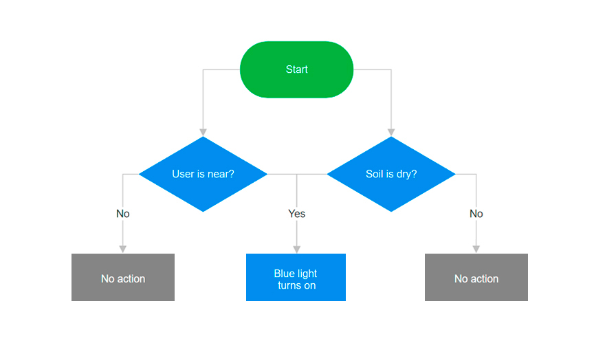
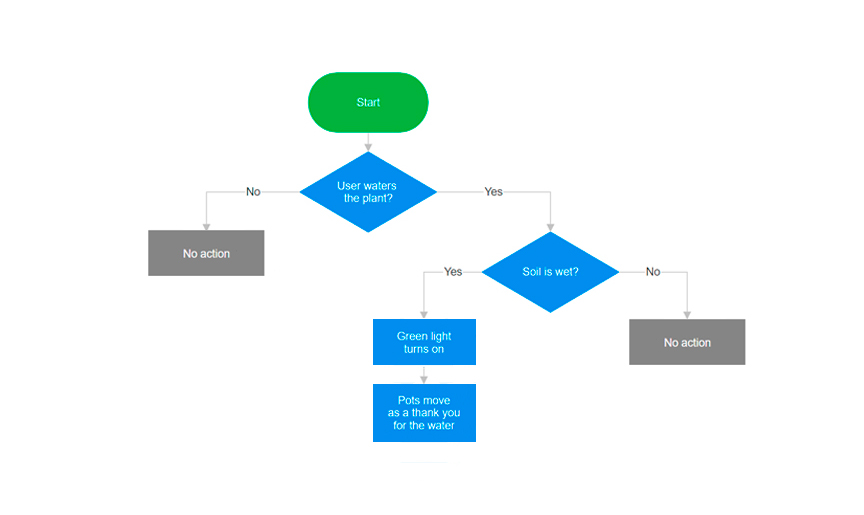
Flowcharts of actions Fab&Plant PCB does
Based on that, I drew a reference diagram of what Fab&Plant PCB would look like.
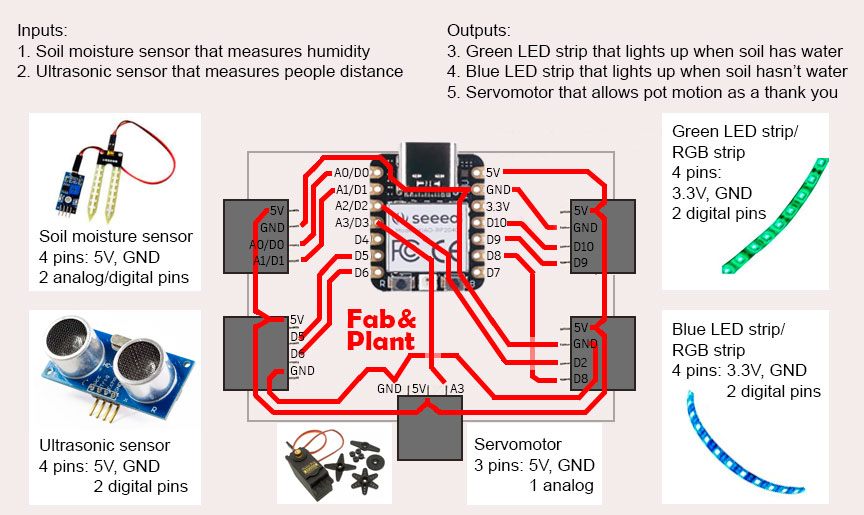
Fab&Plant PCB reference diagram
Having clarity on that point, I started working on my design on the computer.
Designing in KiCad
To design my PCB on the computer, I used KiCad 8. KiCad is an open source software suite for Electronic Design Automation (EDA). The programs handle Schematic Capture, and PCB Layout with Gerber and IPC-2581 output. I chose KiCad because it is an excellent open-source tool with a comprehensive toolset, ease of use, and a strong support community. These features make it attractive to beginners -like me- in electronic design. Compared to other PCB design programs like Altium Designer, Eagle, and OrCAD, KiCad offers a robust alternative without the cost barriers of proprietary licenses.
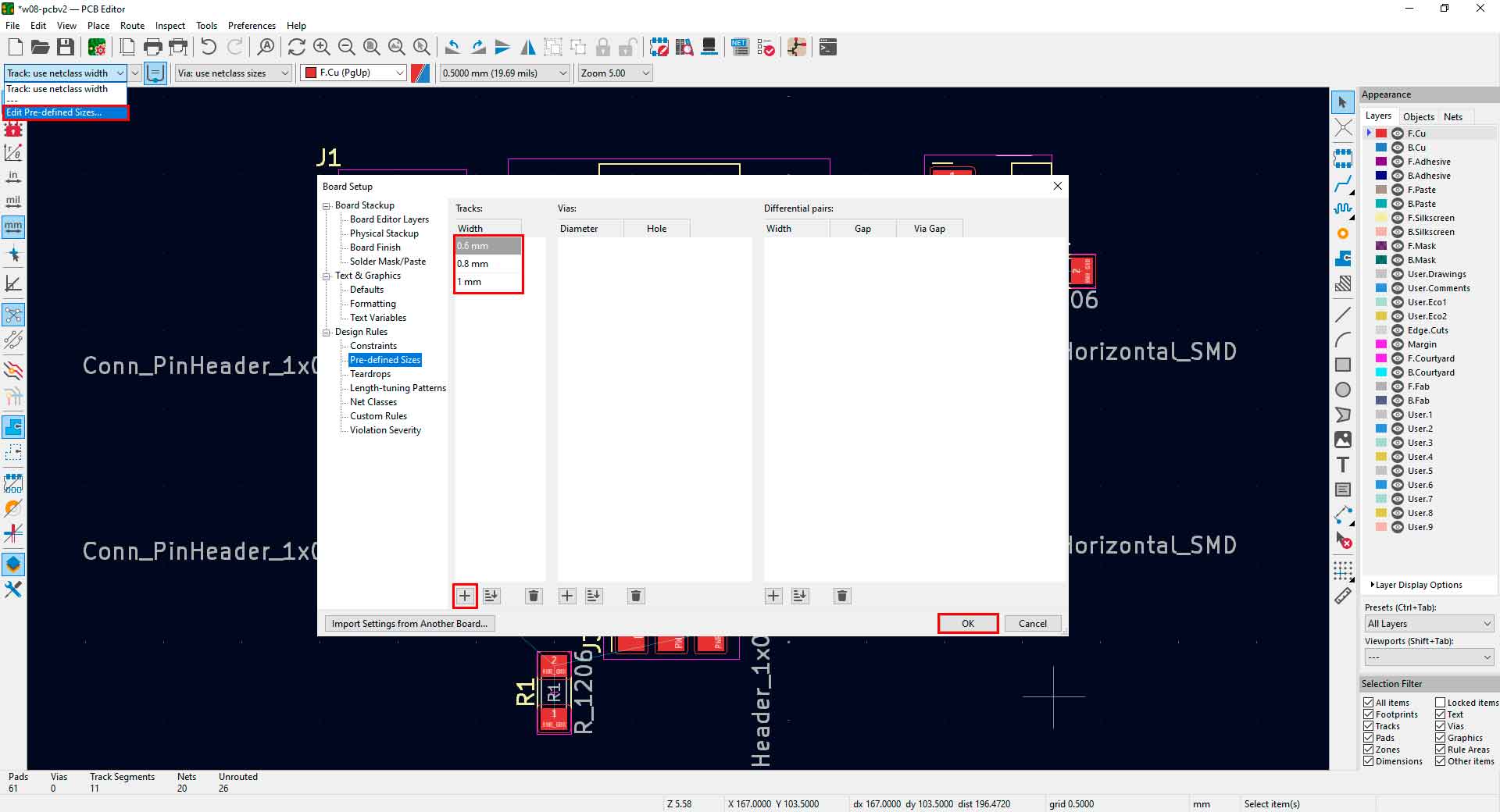
When designing a PCB in KiCad, especially on a copper board, consider the following key design rules:
- Trace width: Determines current capacity and resistance. Wider traces carry more current. In my case, I used 0.8mm.
- Trace spacing: Prevents shorts and electrical interference. In my case, I used 0.5mm.
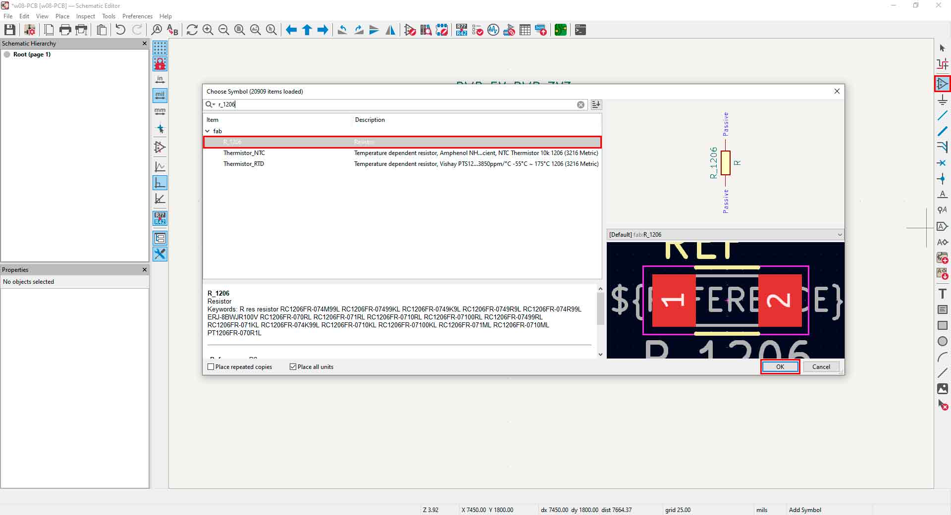
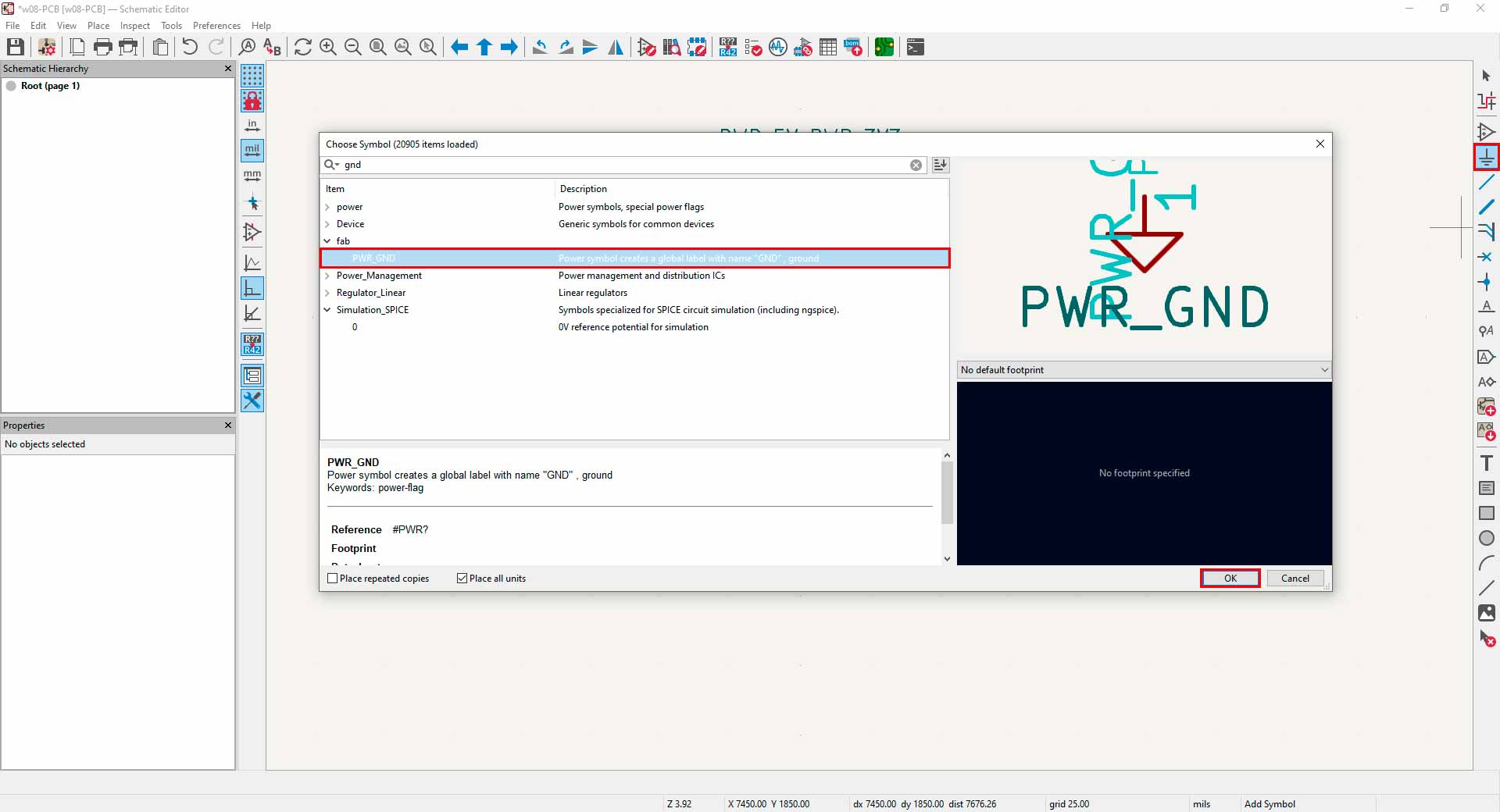
- Pad sizes and SMD footprints: Ensure proper soldering and mechanical stability by following component manufacturer's recommendations. In this case, I used the Fab Academy libray where all the components I used were loaded.
- Clearance: Minimum distance between conductive elements. Standard is around 6 mils (0.15mm), but varies with voltage levels. In my case, I used 2mm.
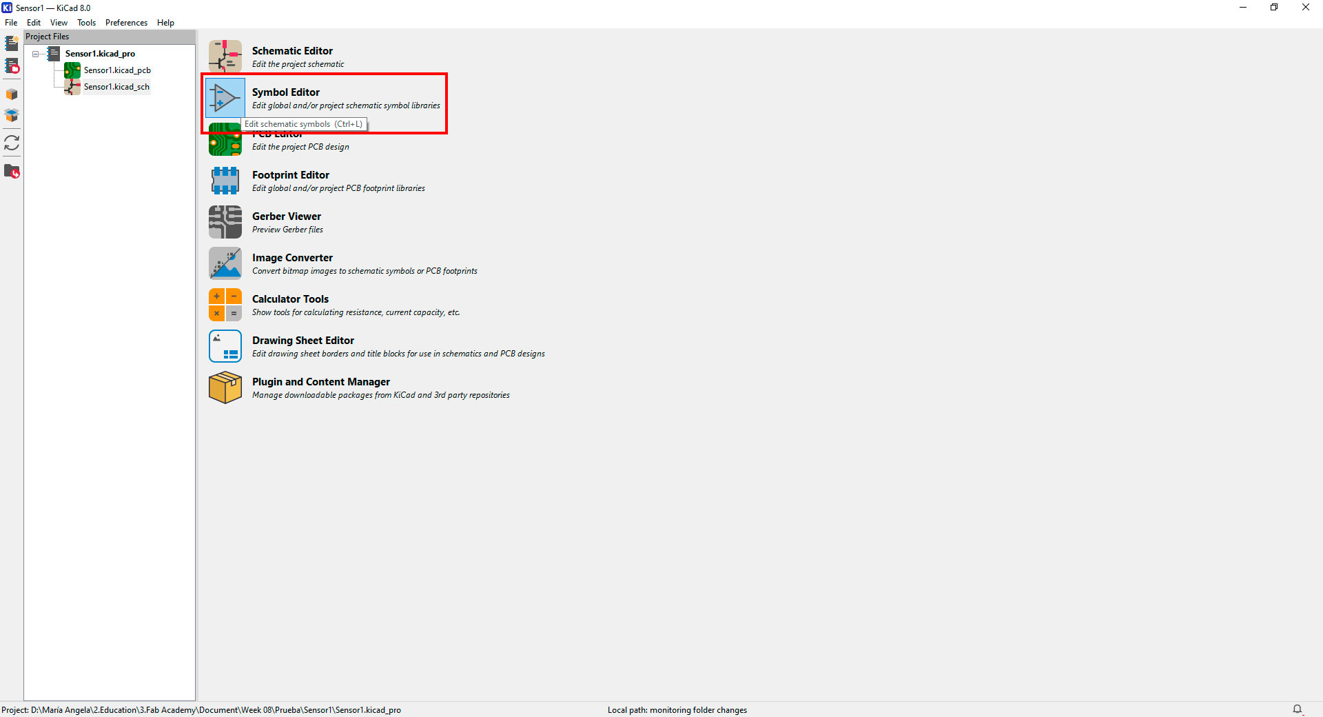
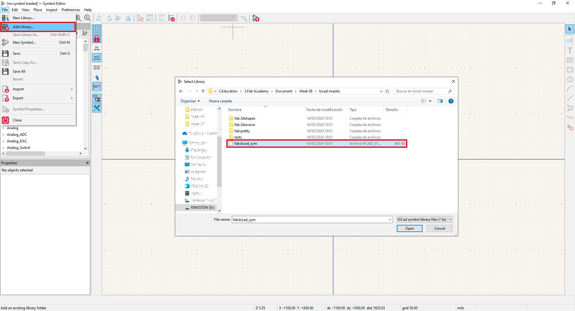
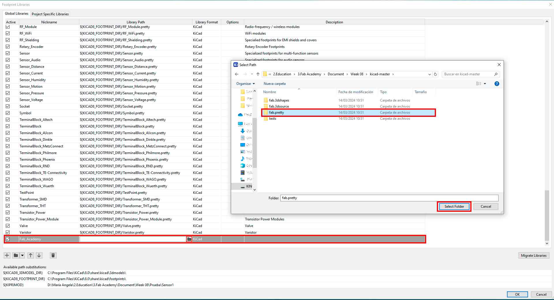
Before starting with the design, I installed the Fab Academy symbol and footprint libraries.
Installing Fab Academy symbol and footprint libraries in KiCad
With that ready, I started the design of Fab&Plant PCB in KiCad.
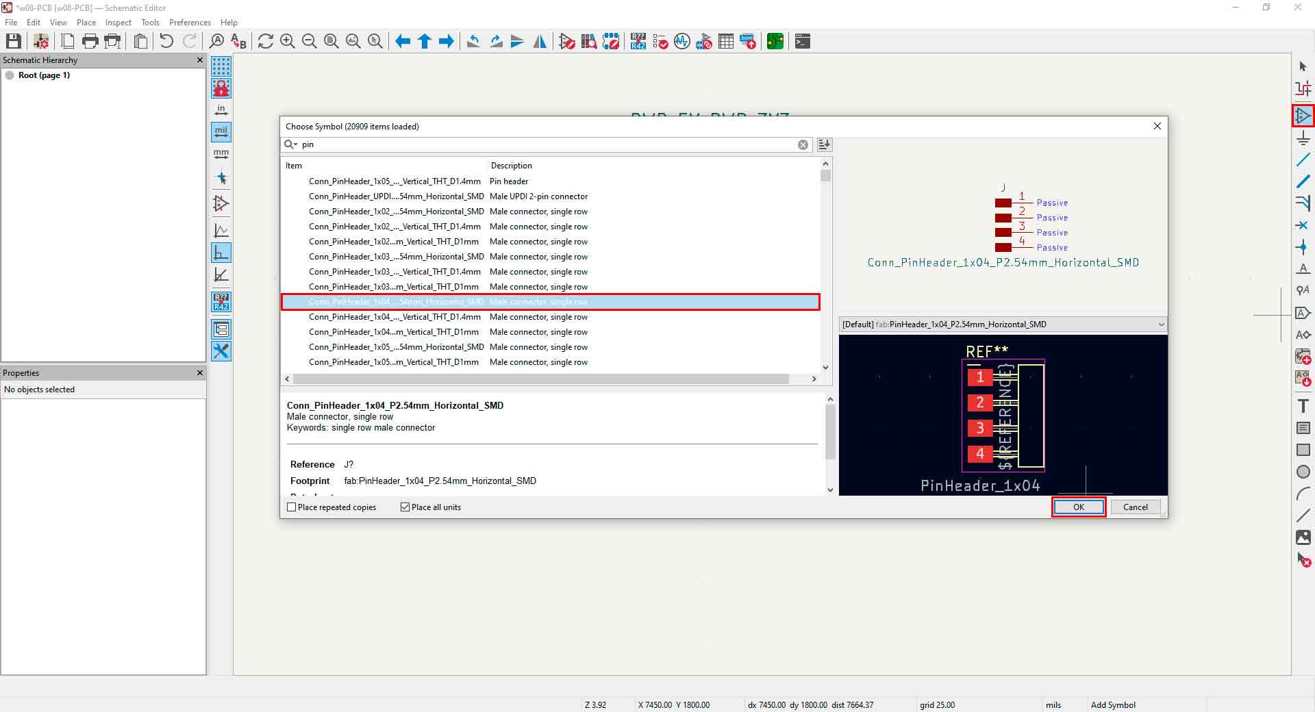
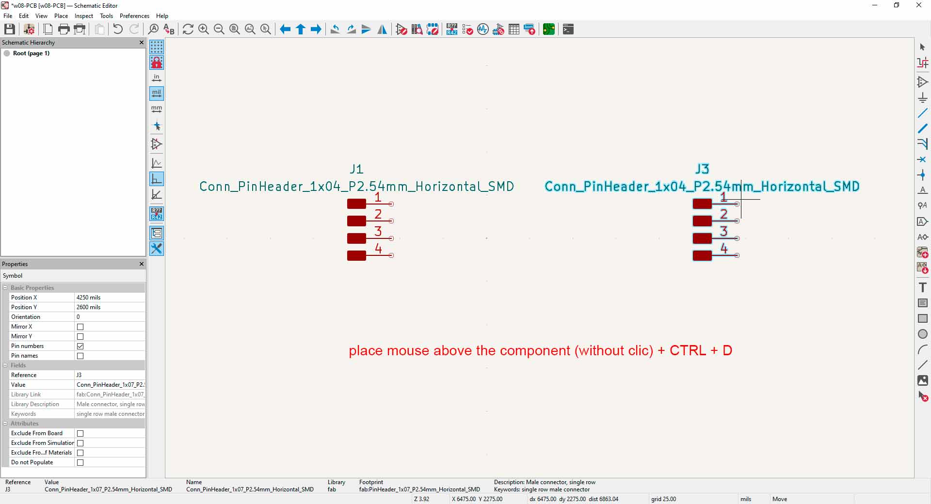
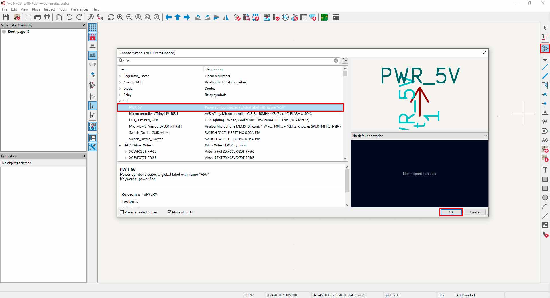
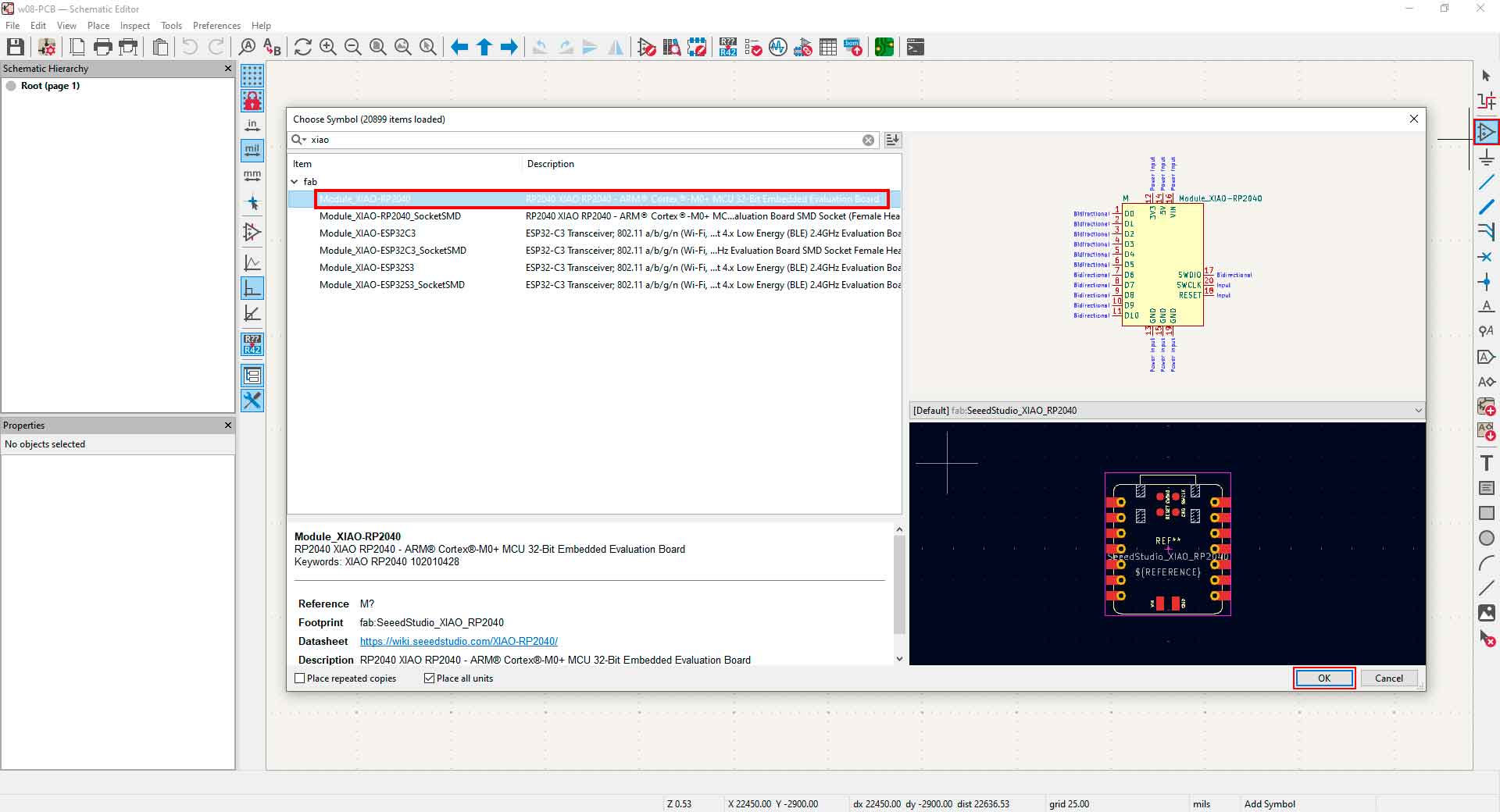
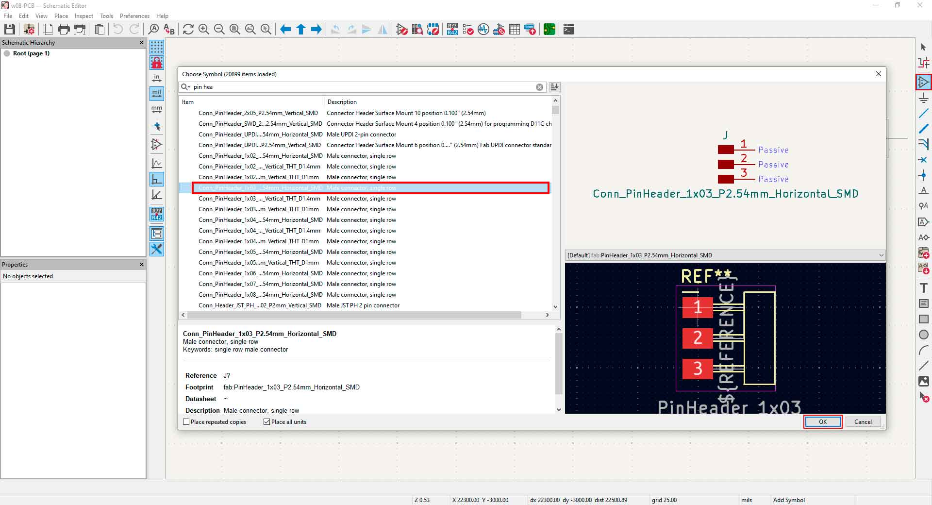
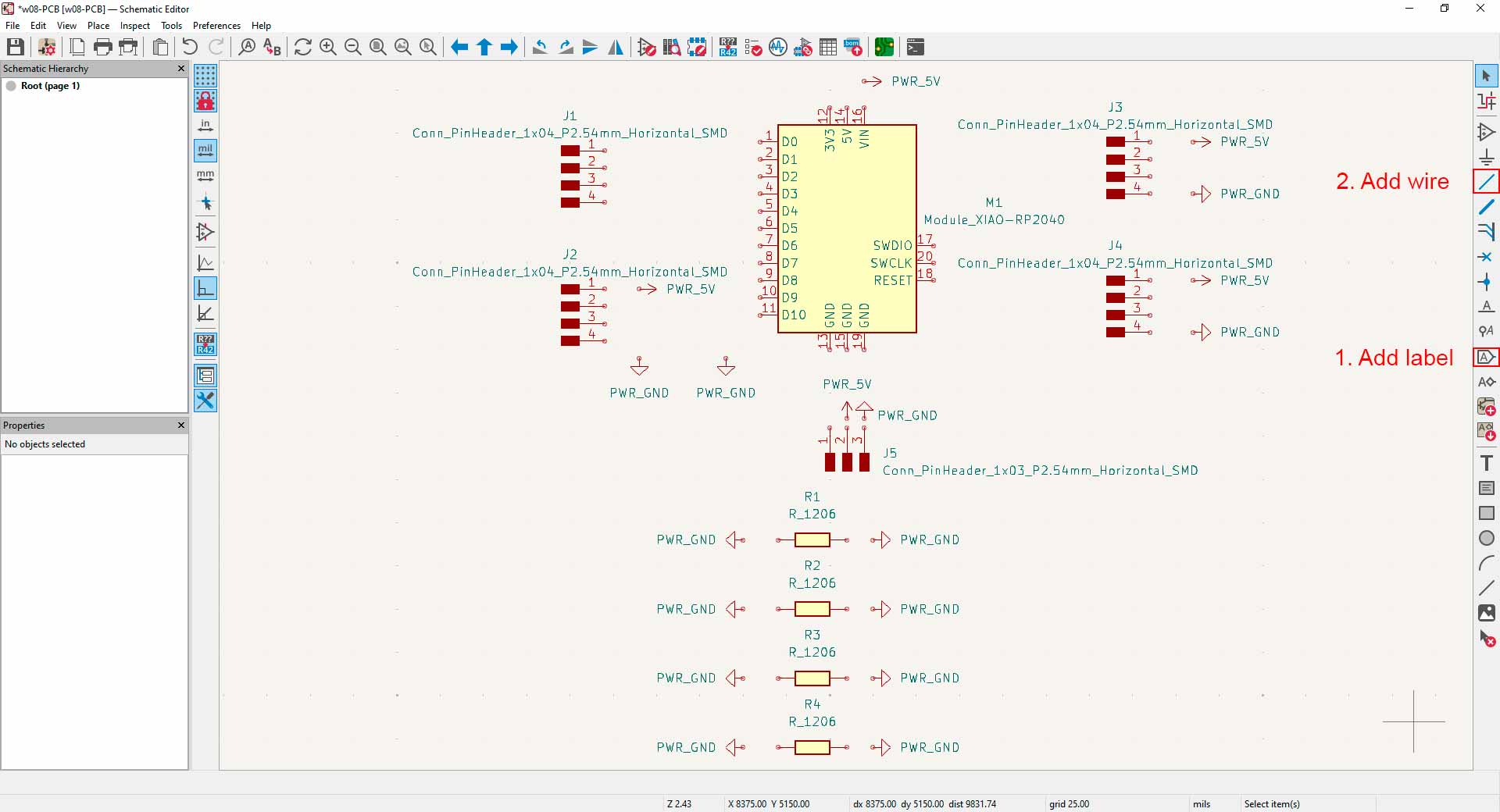
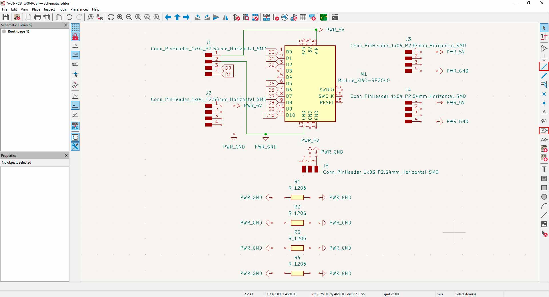
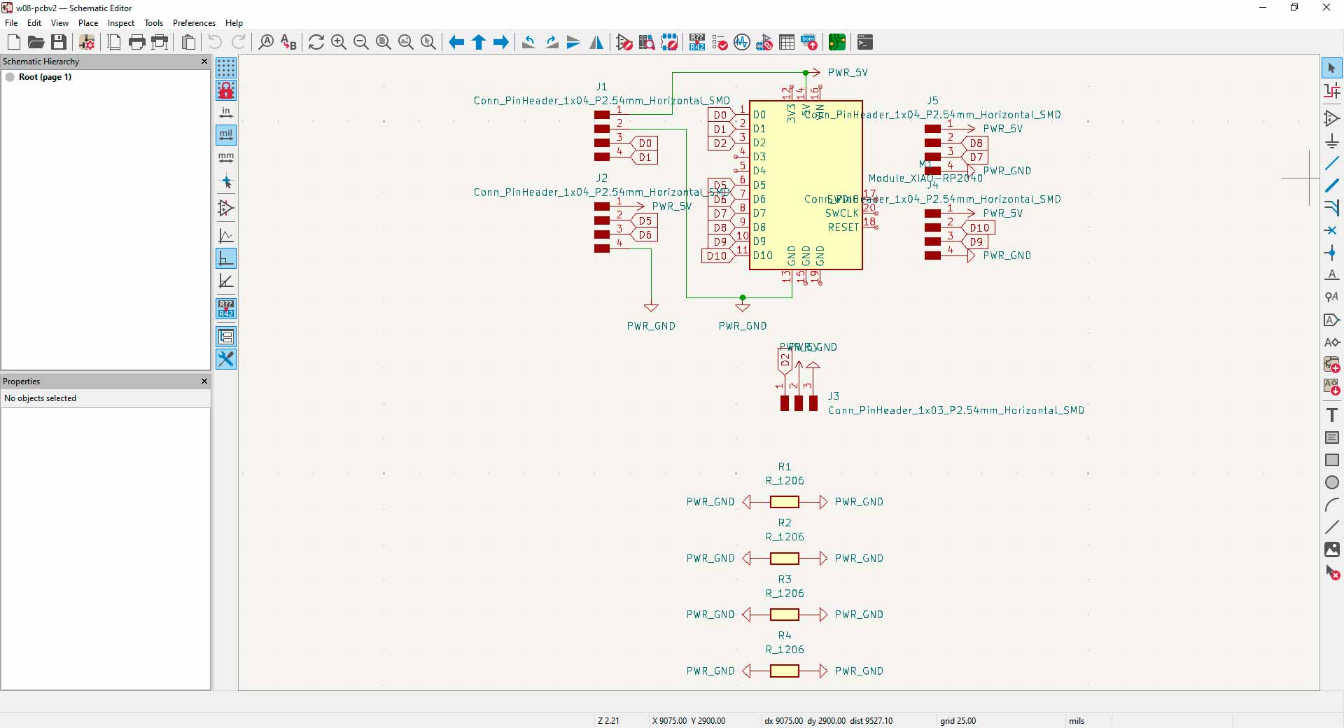
Designing Fab&Plant PCB in schematic editor in KiCad
Finally, I got this result in the schematic editor:
Schematic result in KiCad
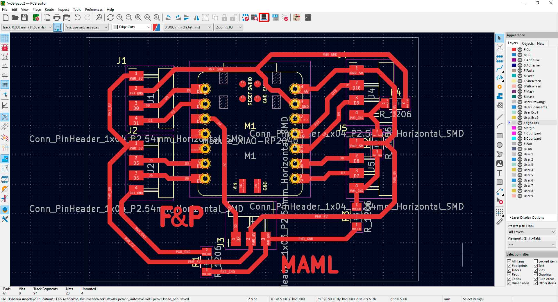
Then, I continued my design in the PCB editor.
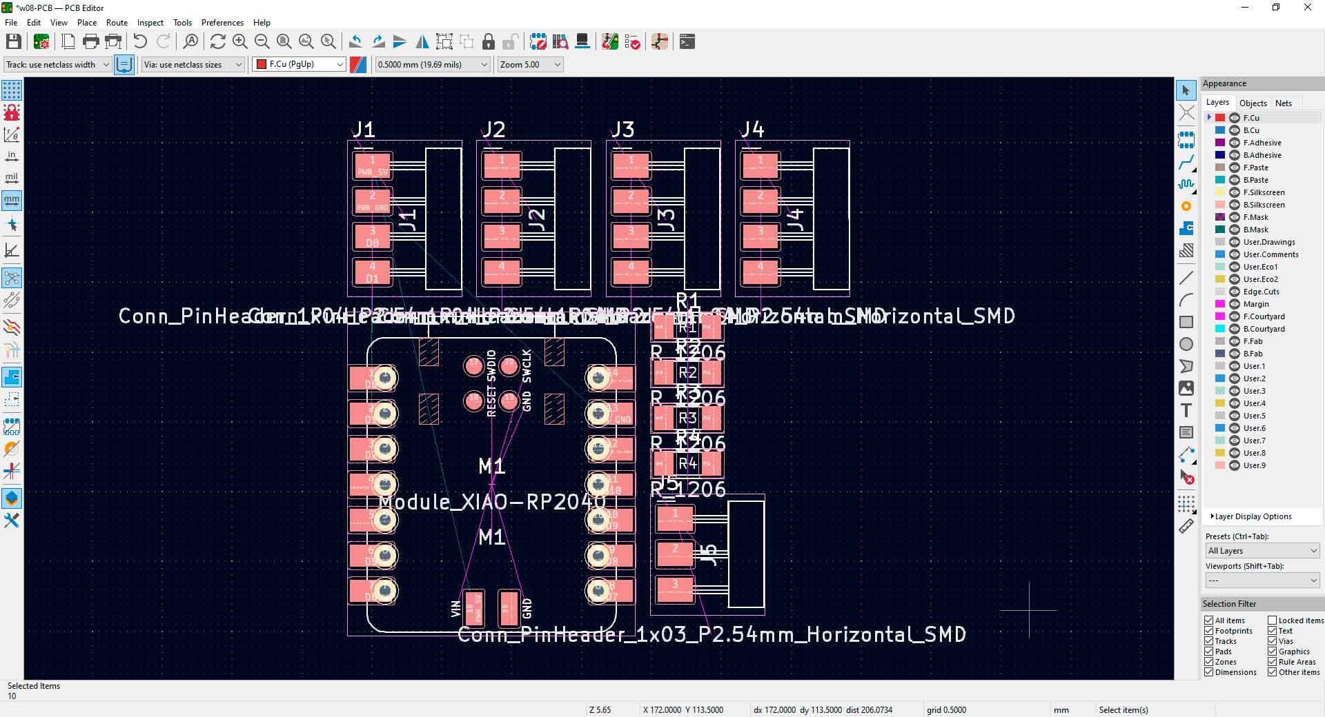
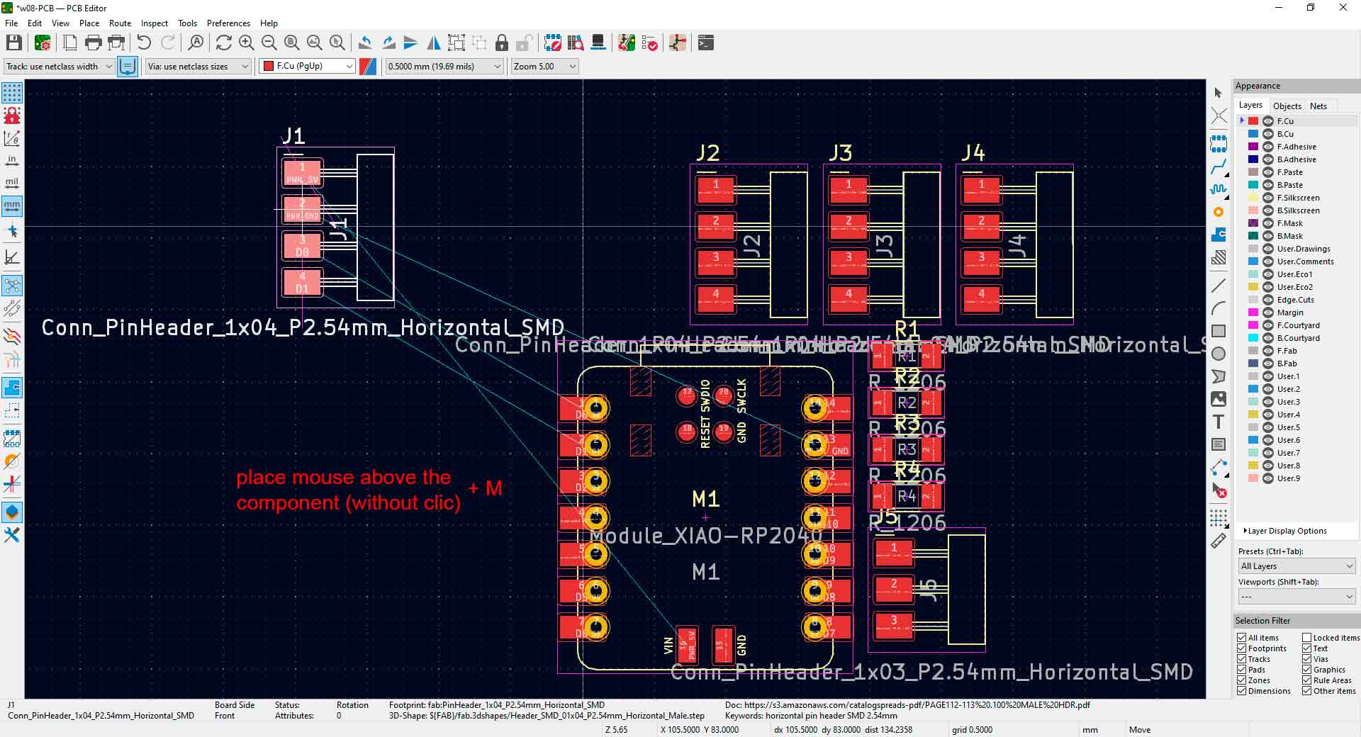
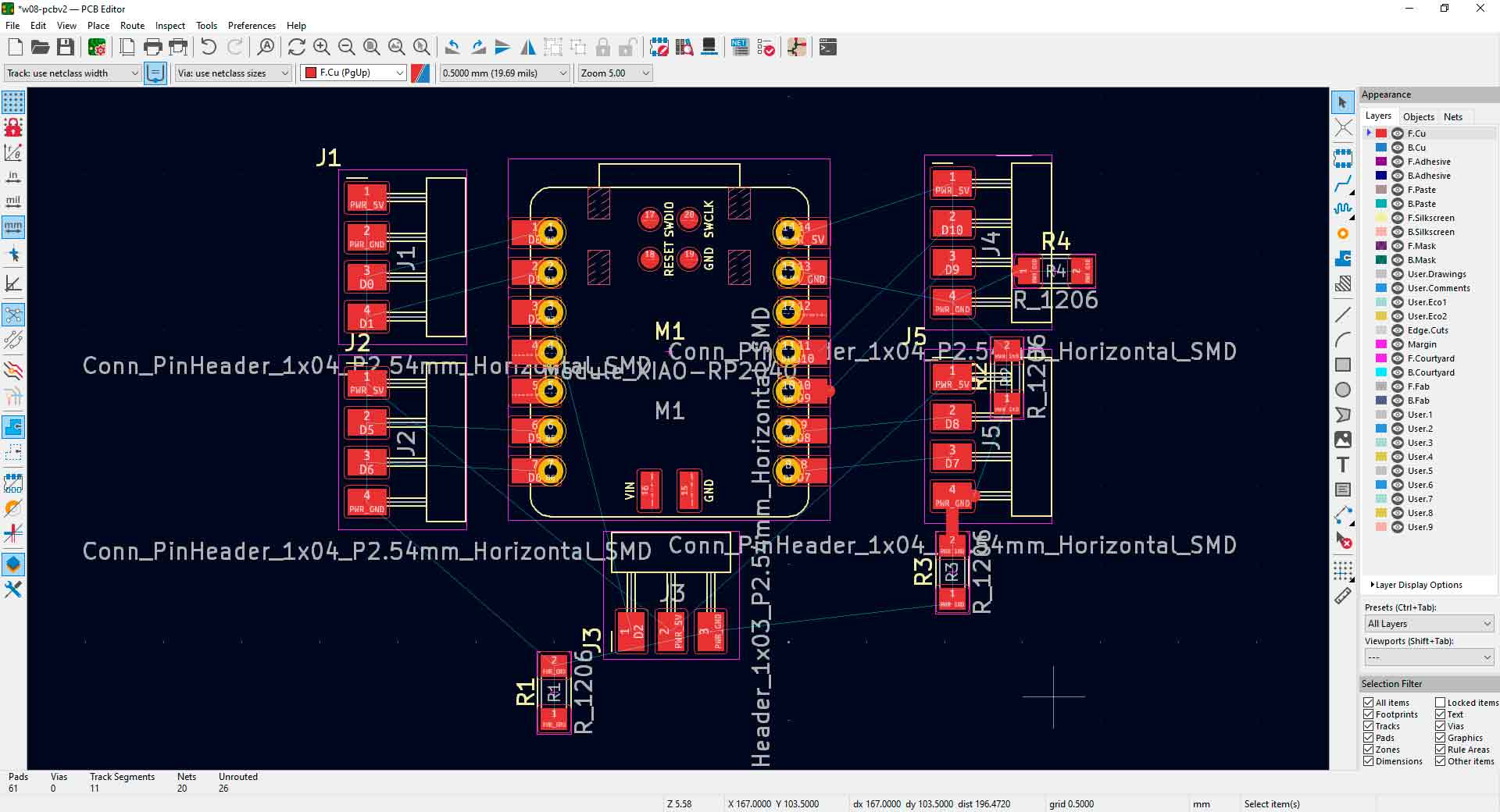
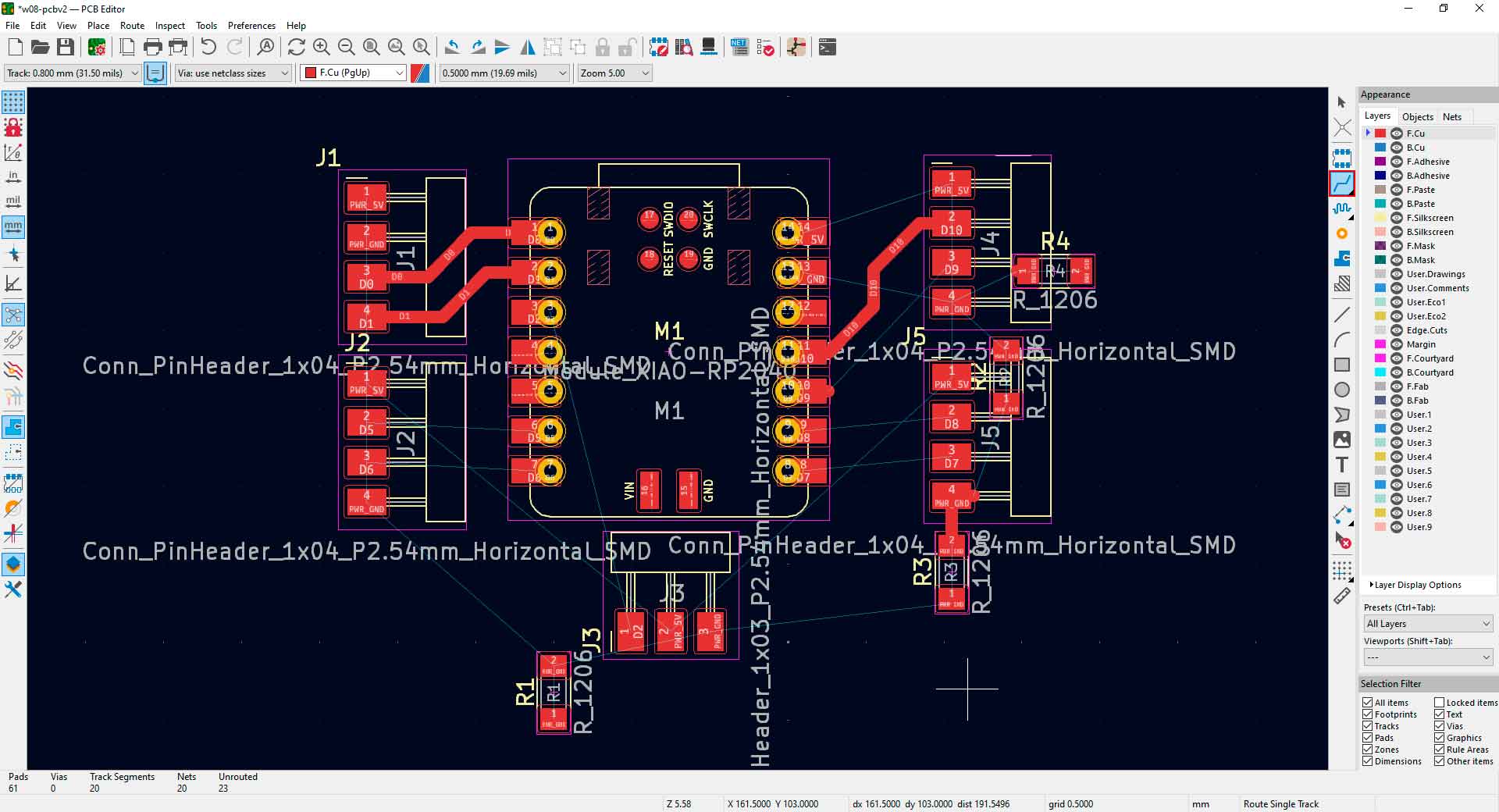
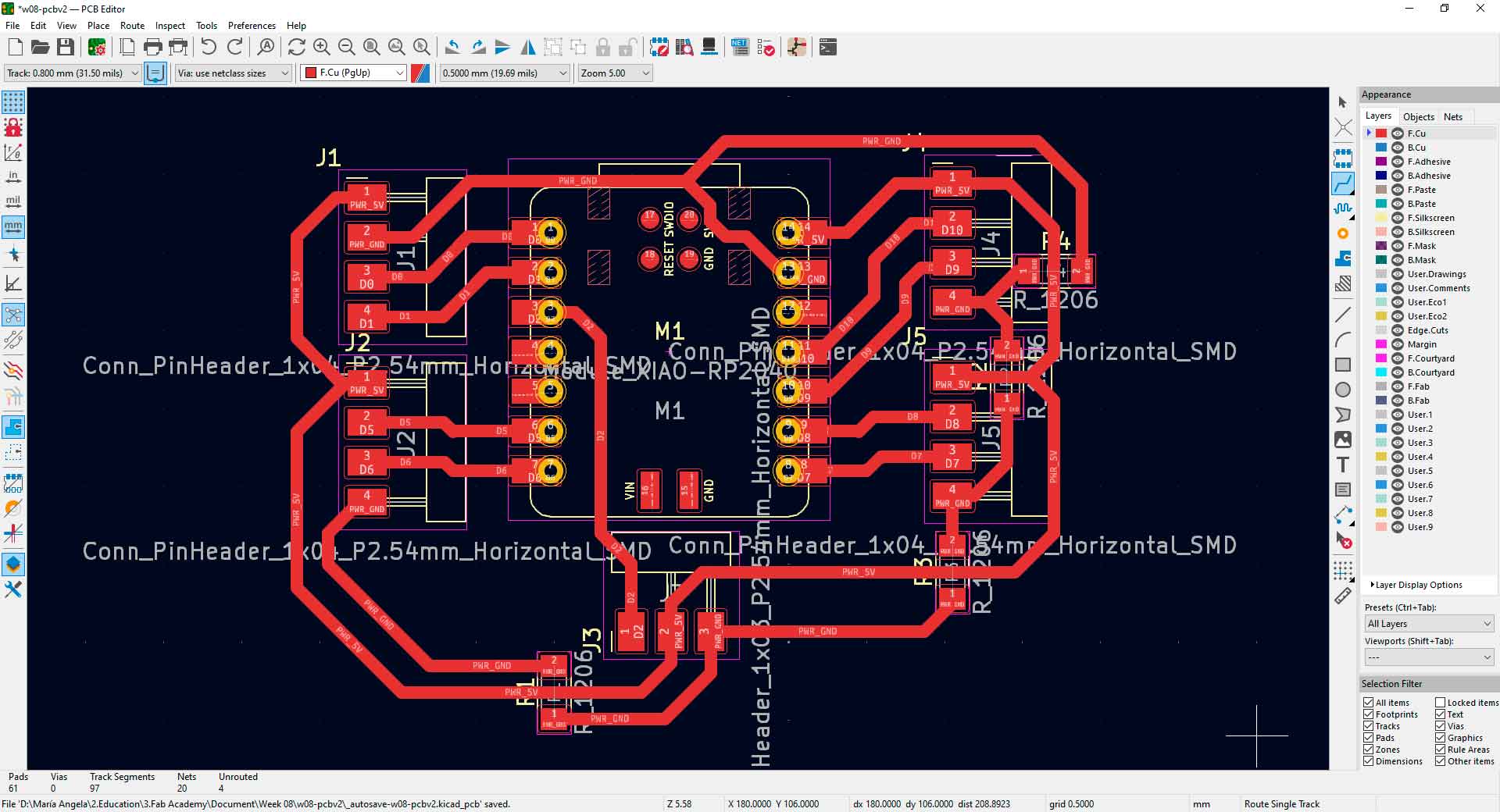
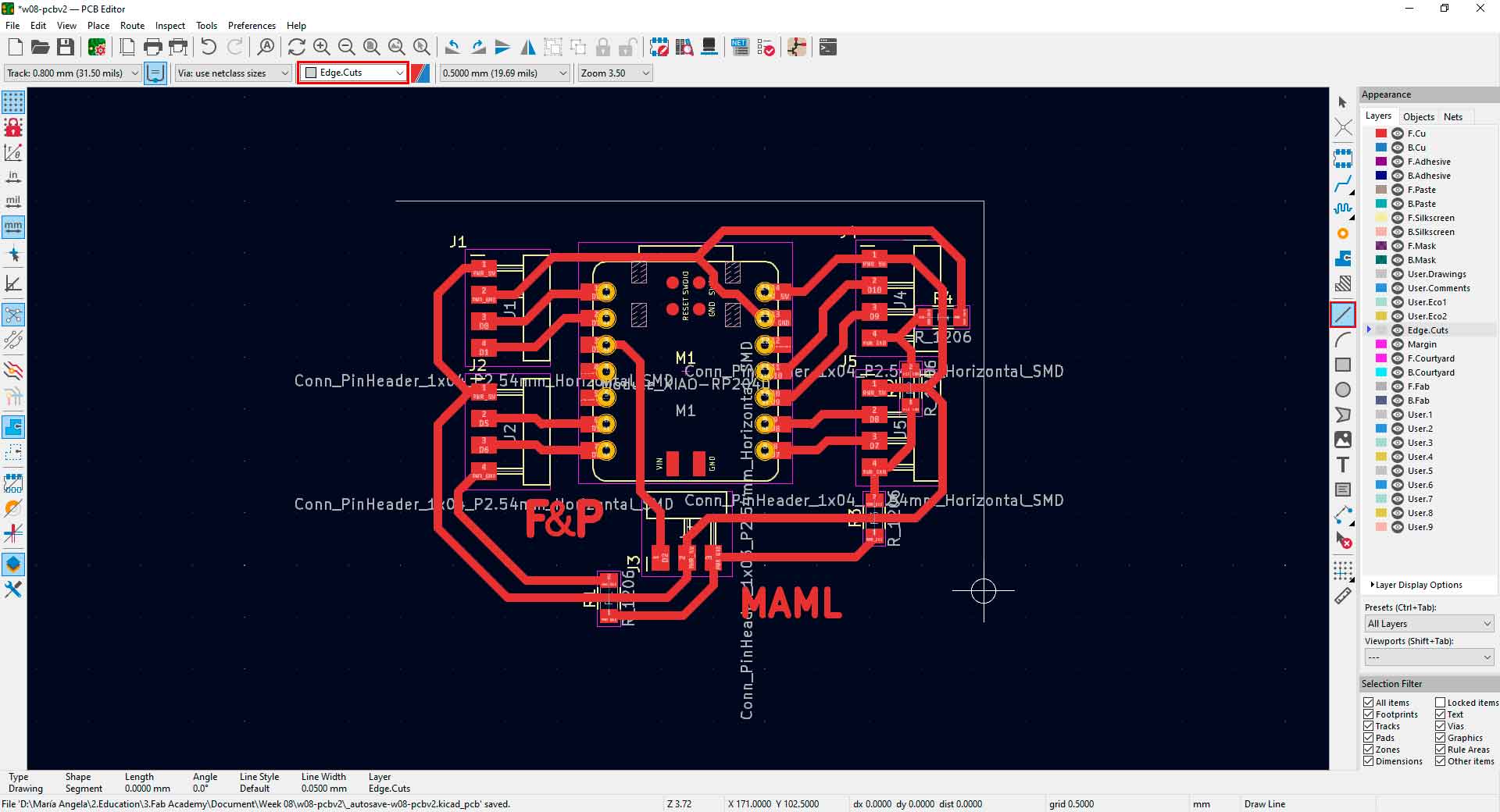
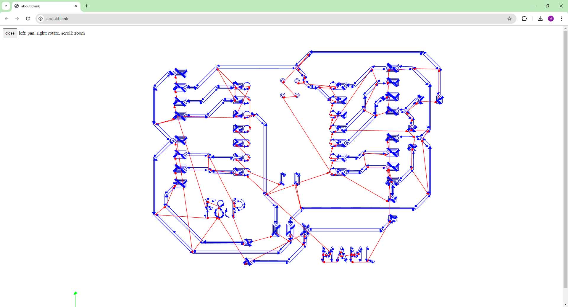
Designing Fab&Plant board in PCB editor in KiCad
Finally, I got this result in the PCB editor:
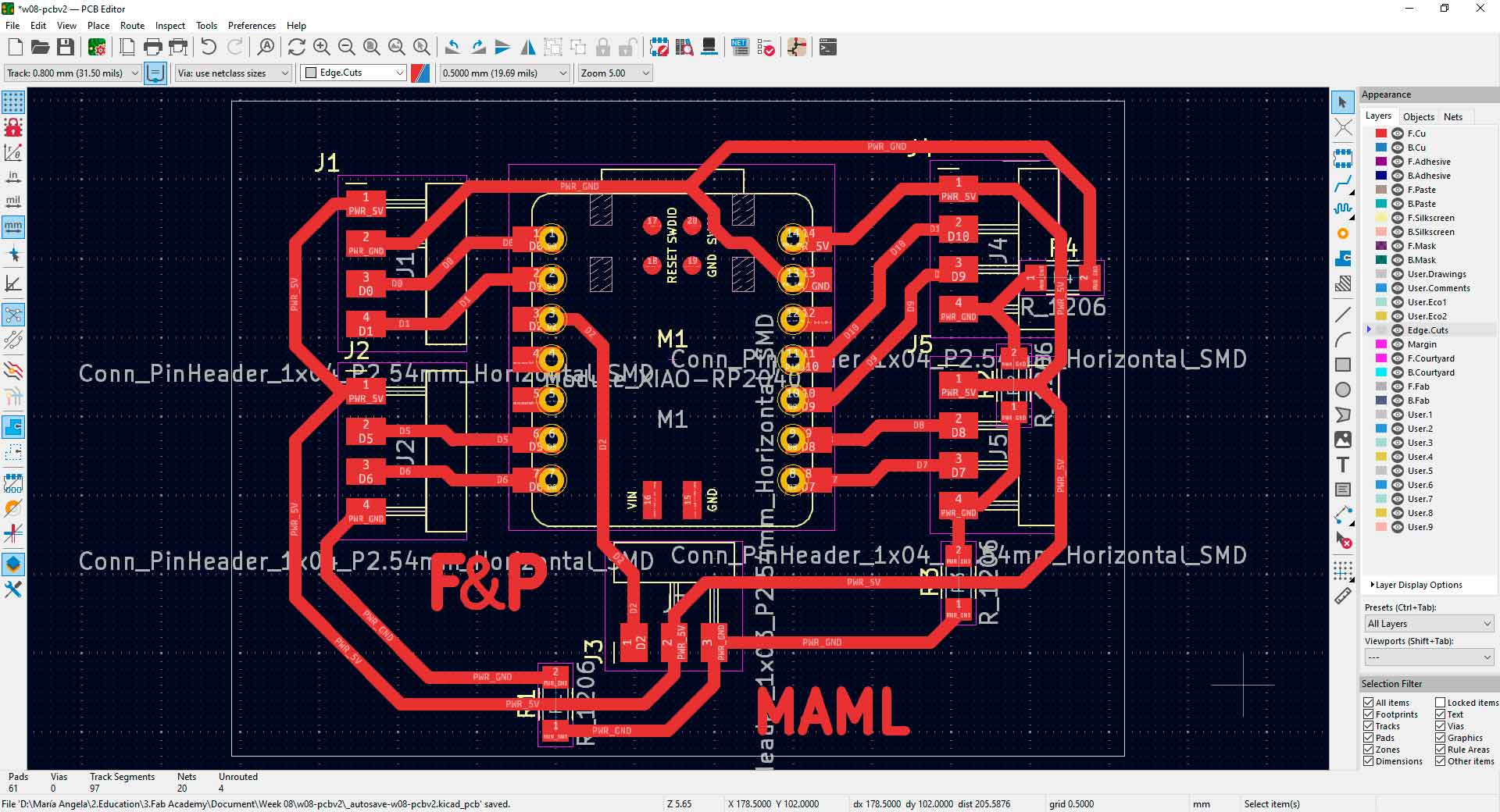
Fab&Plant traces in KiCad PCB editor
Then, I opened the design in the 3D viewer.
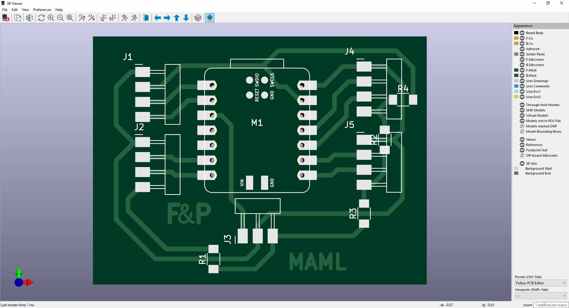
3D viewer in KiCad
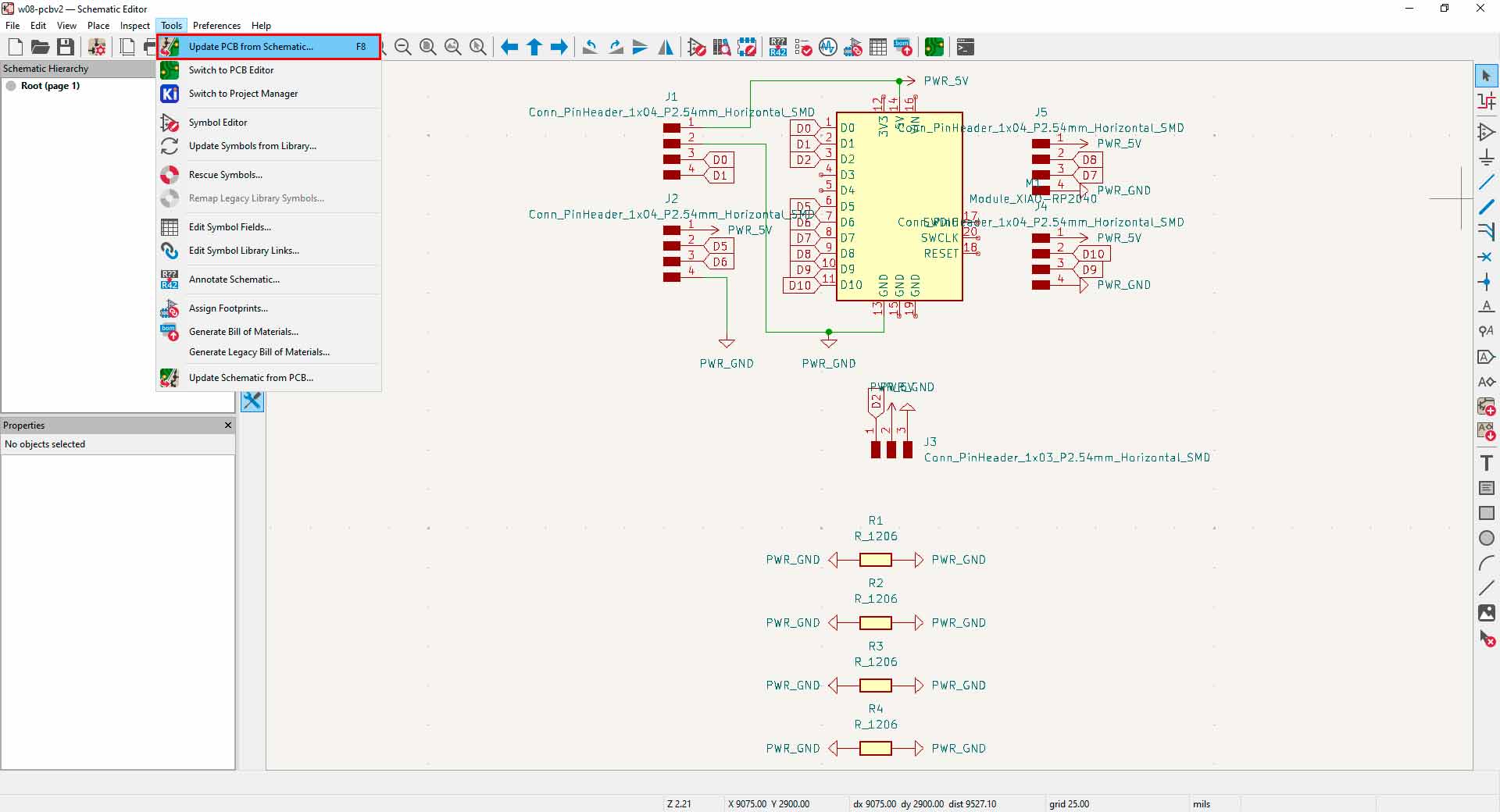
To mill on the Roland SRM-20, I saved my file in .SVG format. To export SVG file in KiCAD:
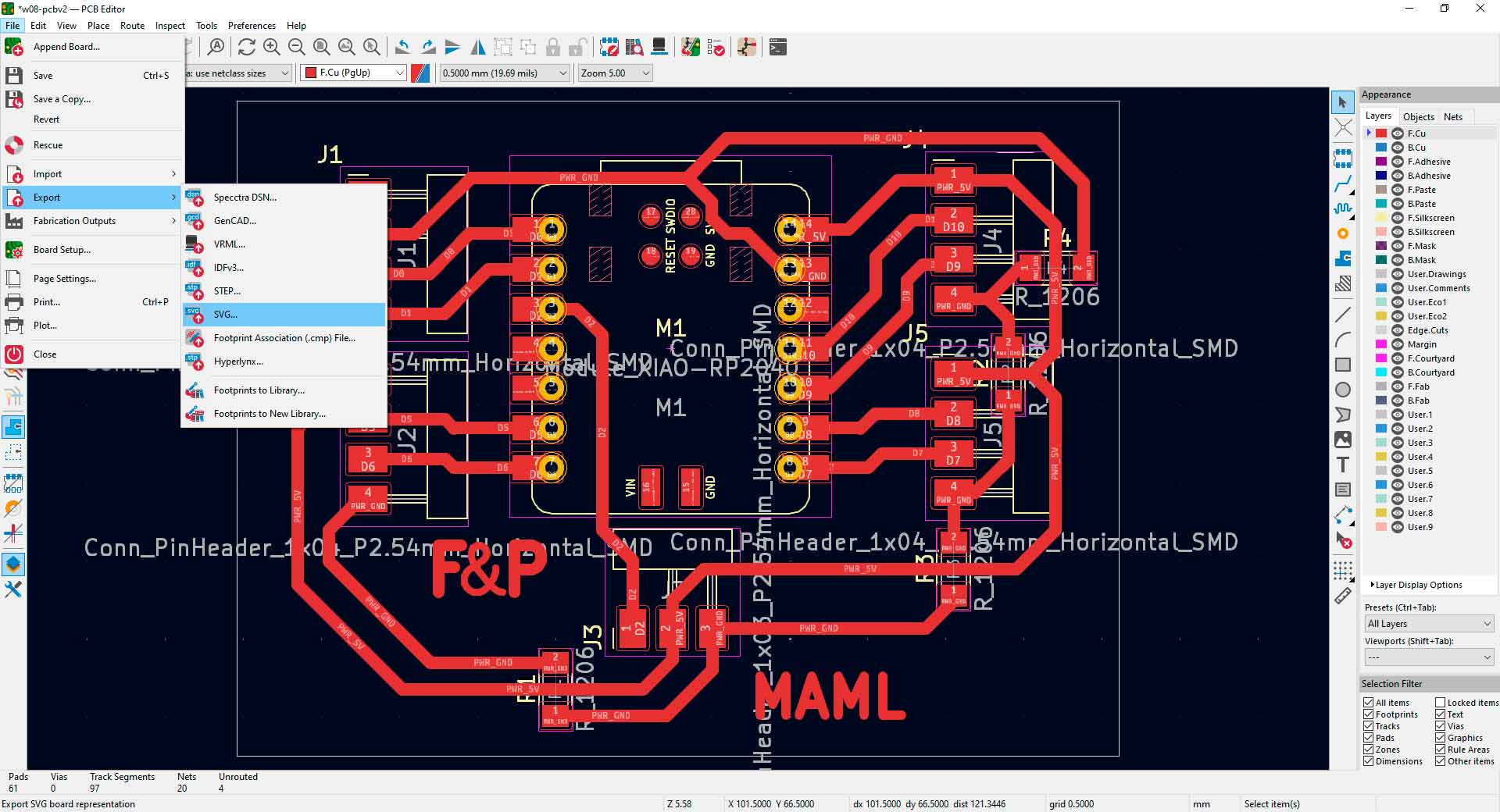
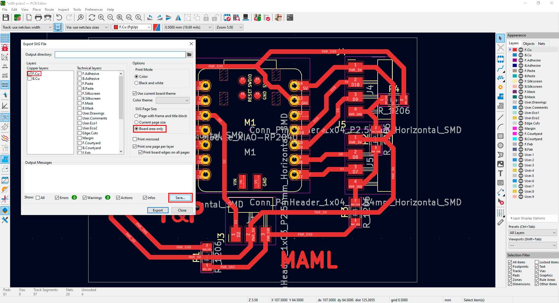
3D viewer in KiCad
With the design ready, I went to the Fab Lab to start milling.
Milling my board
To configure the milling options, I used MODS.
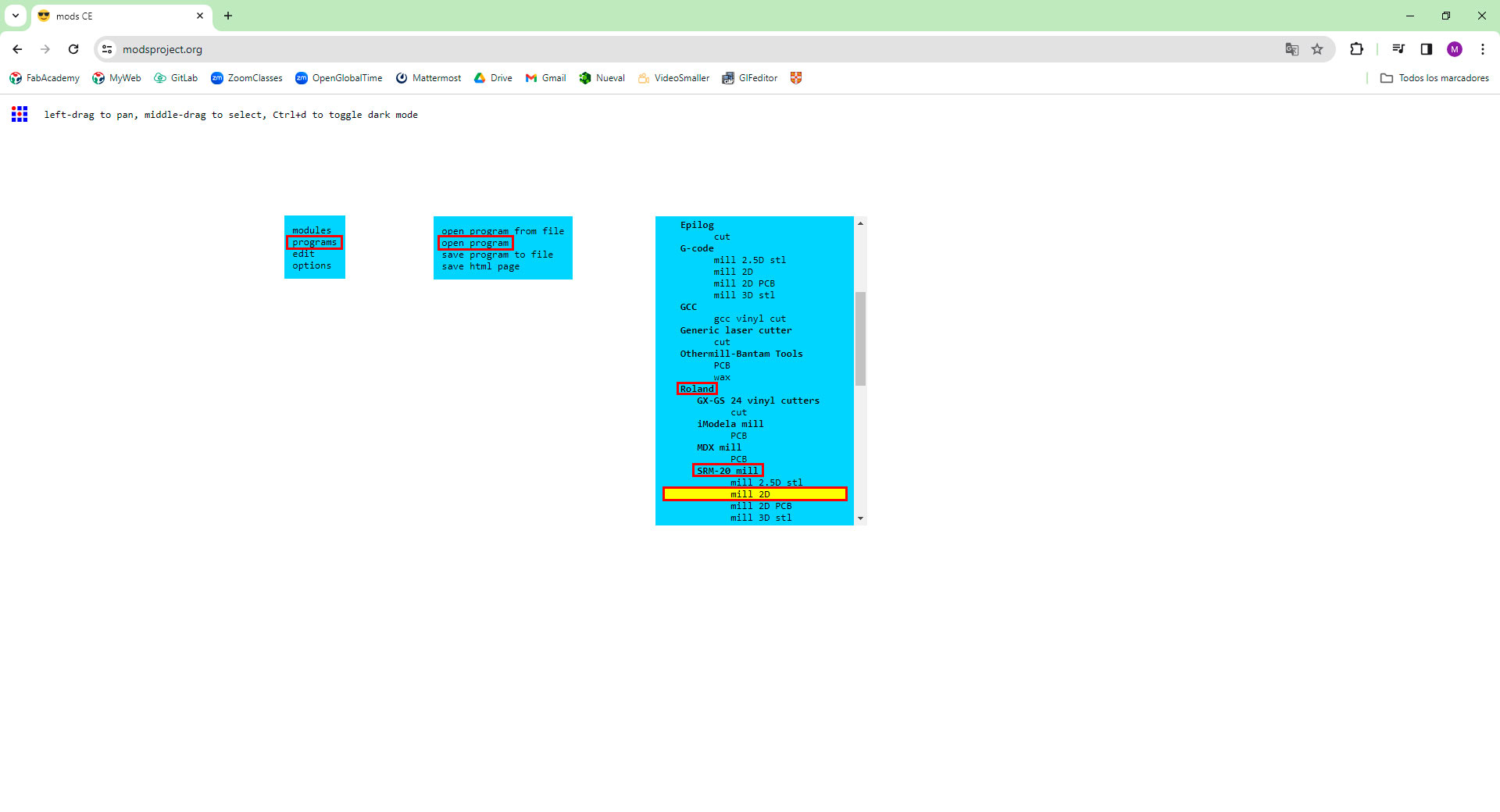
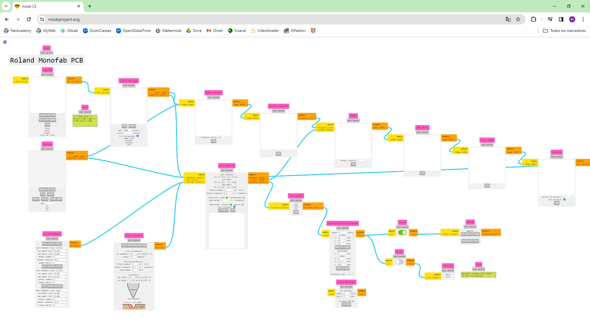
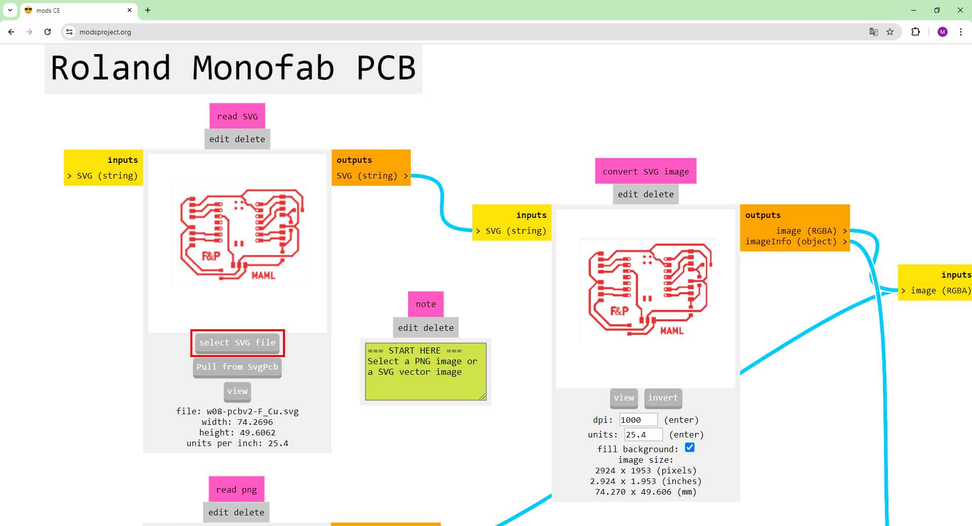
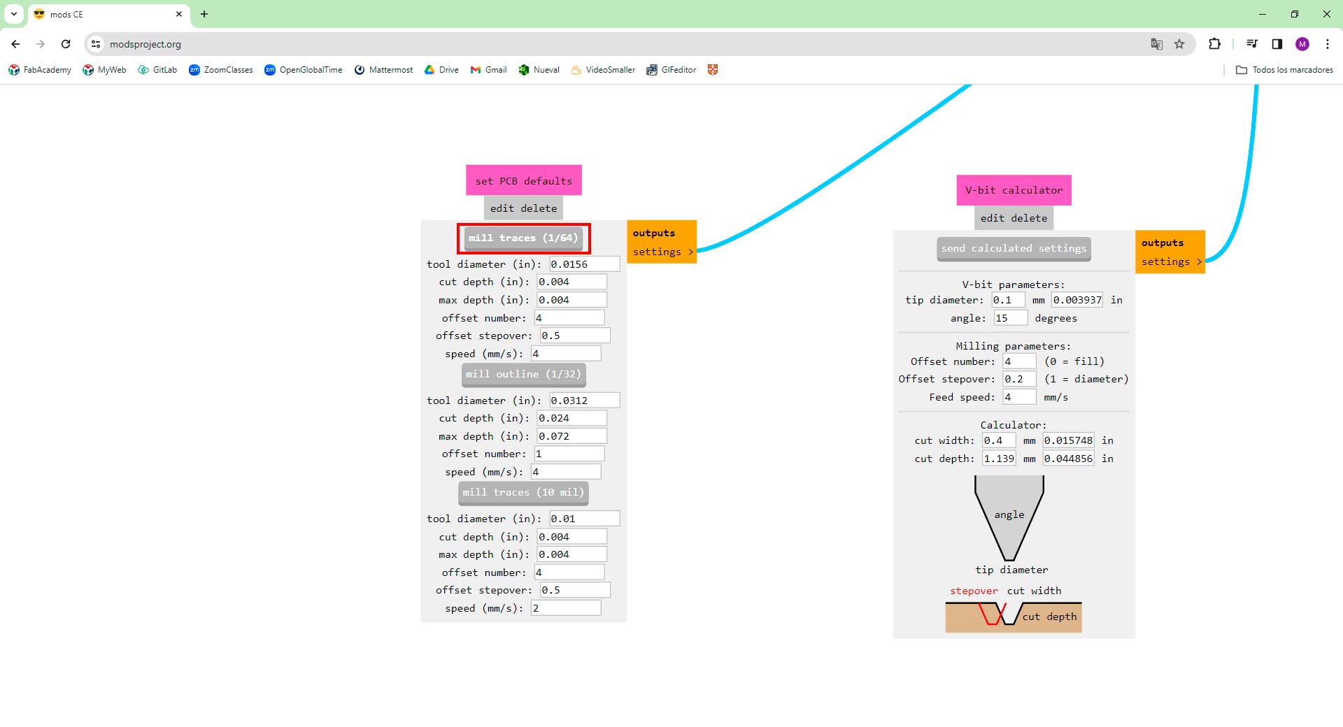

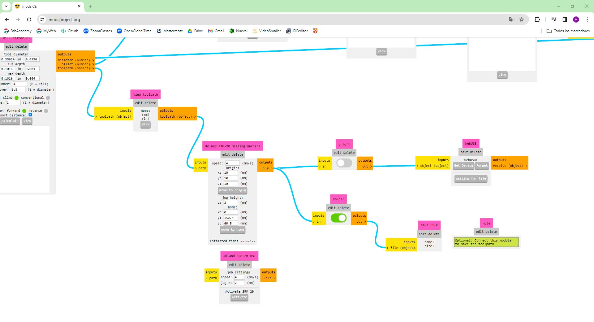
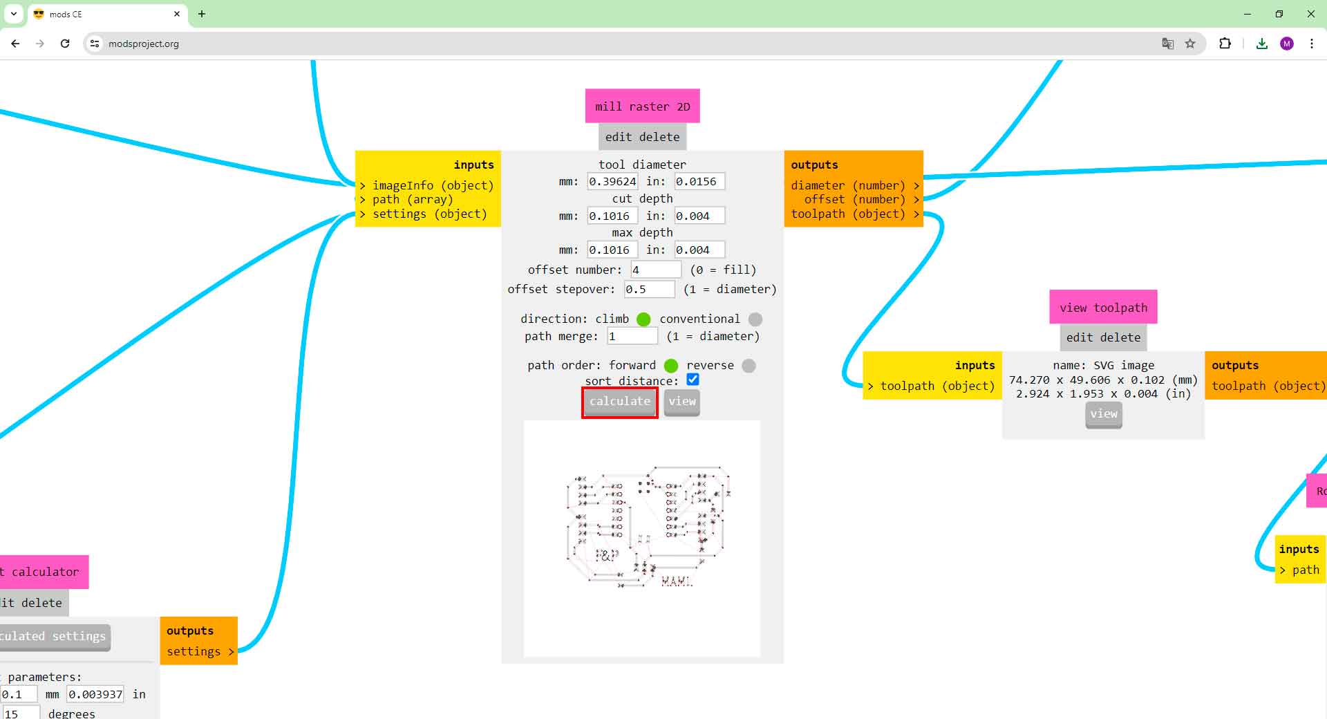
Setup process in MODS to mill my PCB on the Roland SRM-20
Then, the milling began. I used a 1/64 mill for the traces and 1/32 mill for cutting. After 20 minutes, I got my PCB traces ready!
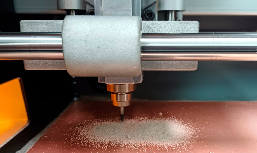
Milling process of my PCB
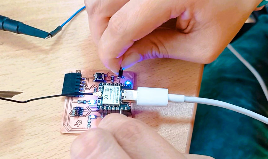
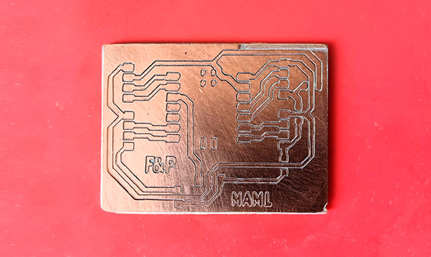
I took it home to start soldering.
Soldering my PCB
At home, I started soldering following these steps:
- Clean the board. First with brush, then scraped on a piece of MDF (to remove burrs). Then, clean it with 300 grit sandpaper (or the finest). Finally, clean it with isopropyl alcohol.
- To start soldering, go over the areas to be soldered with a flux pen (components and board).
- Tin the legs of the components and the corresponding space where they will be located on the board.
- Start by soldering the components that may be more difficult to place. In my case, I started with the 0 resistors. Then, I soldered the components that were too closed to each other.
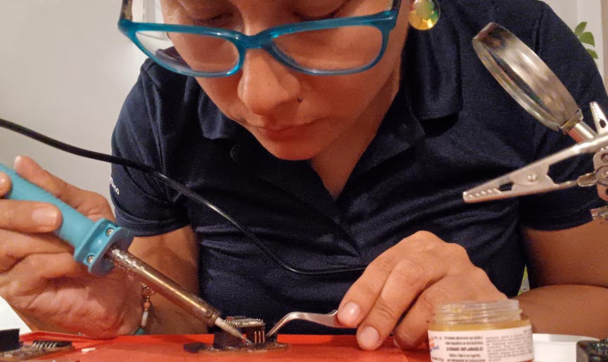
Process of soldering my PCB
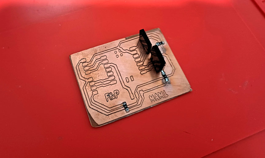
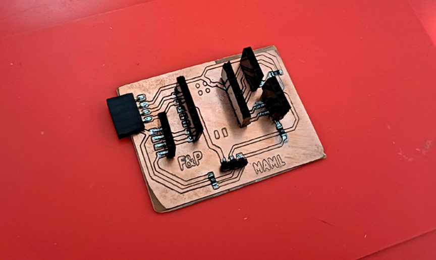
Finally, I present to you my very first PCB!
First Fab&Plant PCB
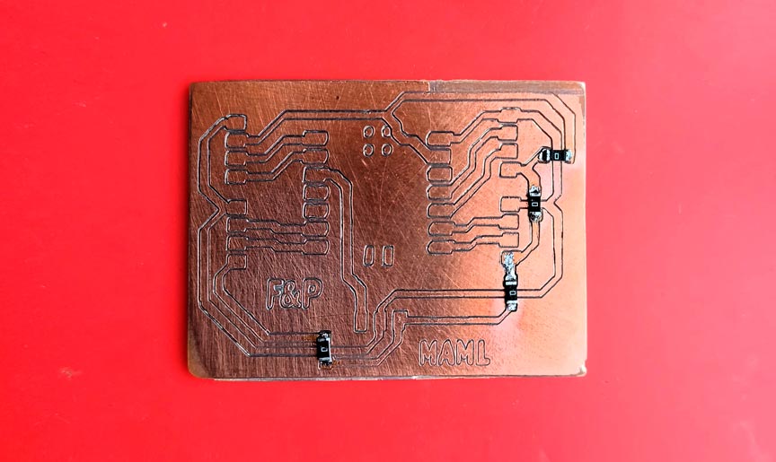
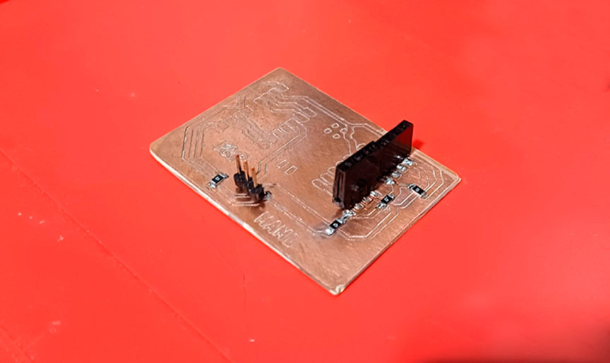
I was very happy to complete this assignment as it was the first time I designed and manufactured my own PCB. Initially, the traces were very thin, making soldering difficult. Over the next few weeks, I created a second version with a larger gap between the traces.
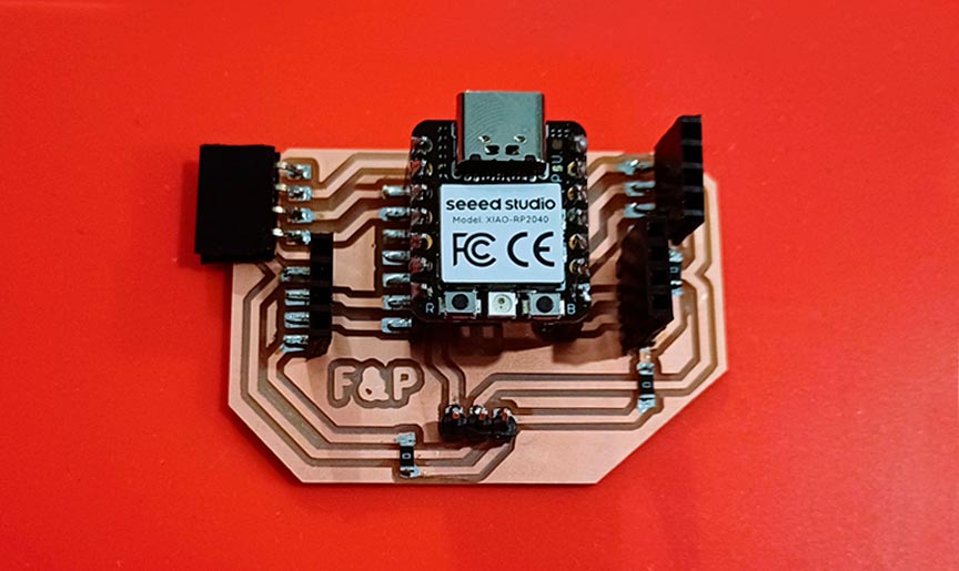
Second Fab&Plant PCB
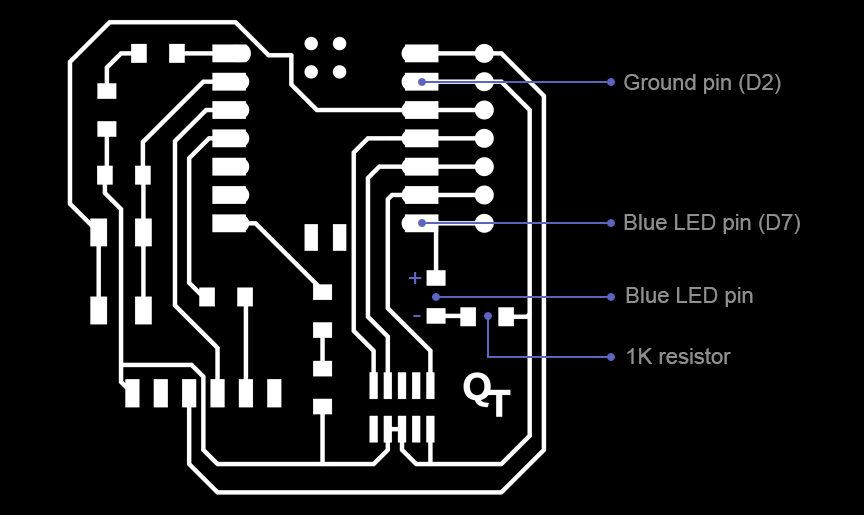
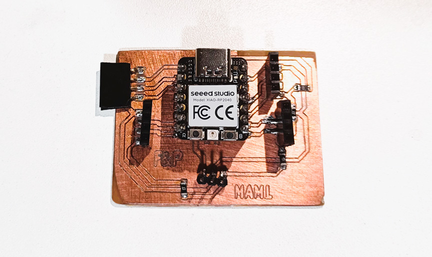
Programming my PCB
I connected the hygrometer I tested in week 6 and programmed XIAO RP2040 microcontroller in Fab&Plant PCB. I used this code in Arduino IDE:
// constants
const int hygrometer = A2;  // hygrometer sensor analog pin output at pin A2 of XIAO RP2040
// variables
int value;

void setup(){

  Serial.begin(9600);
}

void loop(){
  // when the plant is watered well the sensor will read a value 380∼400, I will keep the 400
  // value but if you want you can change it below.

  value = analogRead(hygrometer);     // read analog value
  value = constrain(value,400,1023);  // keep the ranges
  value = map(value,400,1023,100,0);  // map value: 400 will be 100 and 1023 will be 0
  Serial.print("Soil humidity: ");
  Serial.print(value);
  Serial.println("%");
  delay(10000);                       // read every 10 seconds
}
Code in Arduino IDE for programming hygrometer in Fab&Plant PCB
Code well programmed
The task for this week was really intense: I did the work of week 04 and 06 in one week!
Conclusions
- Starting with a clear diagram of my PCB's goals and components was crucial. It helped visualize the end product and ensured that all necessary elements were considered before diving into the design phase.
- Learning how to use software like KiCAD proficiently was essential for efficient and effective PCB design. Familiarizing myself with the tools available and understanding their functions can streamline the design process and minimize errors.
- Soldering components onto a PCB required precision and attention to detail. Ensuring that each component was correctly placed and soldered can prevent connectivity issues and ensure the functionality of the final product.
- Like any skill, PCB design and soldering require practice to master. Don't be discouraged by initial setbacks or mistakes; instead, view them as opportunities to learn and improve your skills.
- Programming and testing my PCB after soldering was crucial to identify any potential errors or malfunctions. This step allowed me to debug and troubleshoot my design, ensuring that it meets the intended functionality.
- To finish this task I thank my fellow students and tutors, especially Roberto Delgado and Ulises Gordillo for the guidance in this process, Silvana Espinoza and Hans Moncca for helping me with the use of the milling machine and valuable tips on PCB design.