8. Electronics Production
Our assignments this week are all about using the table top fine milling machine to mill printed circuit boards (PCB) that will interact with our embedded microontroller.
Group Assignment
Our group assignment this week was to characterize the design rules for our in-house PCB production process. We would receive extra credit if we sent our PCB out to a board house.
The link to our group work page can be found here.
Group Results
This week, we needed to characterize our in-house milling machine for PCB production.
- Model: ForestCNC ATC CNC.
- Software: Vectric Cut2D Pro.
- Tools: 1/64 end mill, 10 degree engraving bit, 15 degree engraving bit.
- Material: FR-1 PCB Board.
General Process:
- Design your PCB in Kicad.
- Export the plotted Kicad File from PCB Editor as a DXF File.
- Open DXF file in Cut2D Pro.
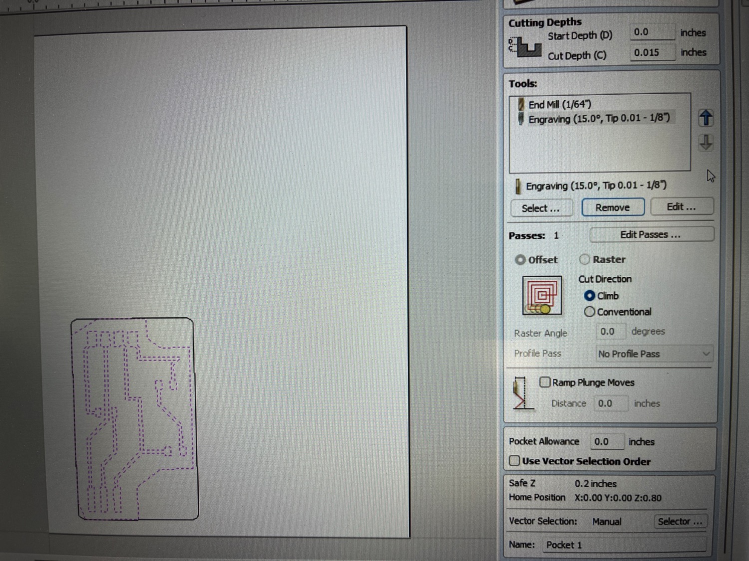
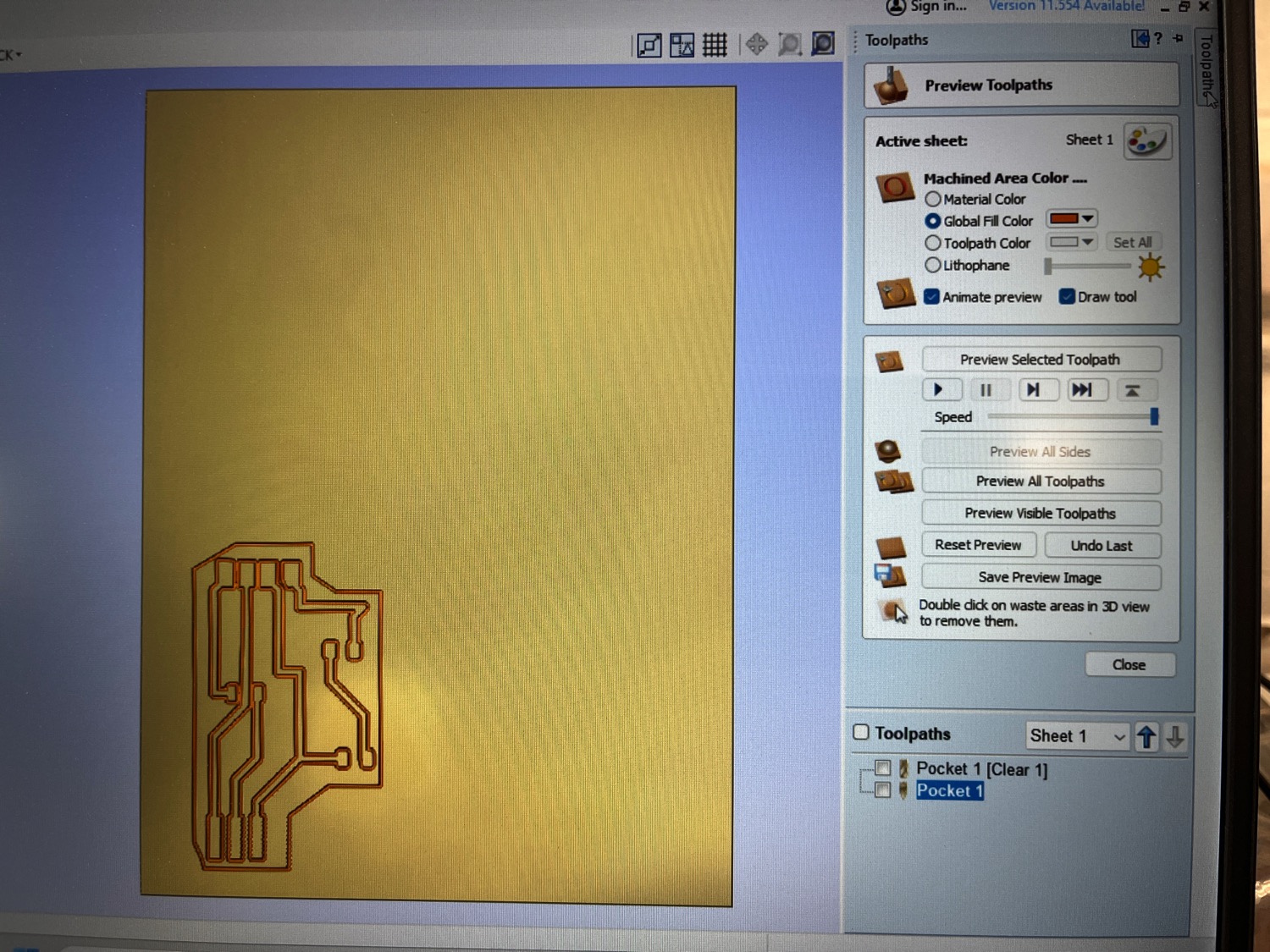
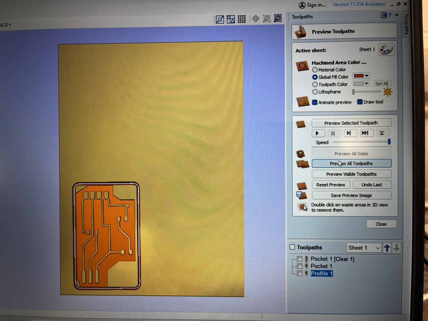
- Create a pocket toolpath for the traces. Reference the images below.
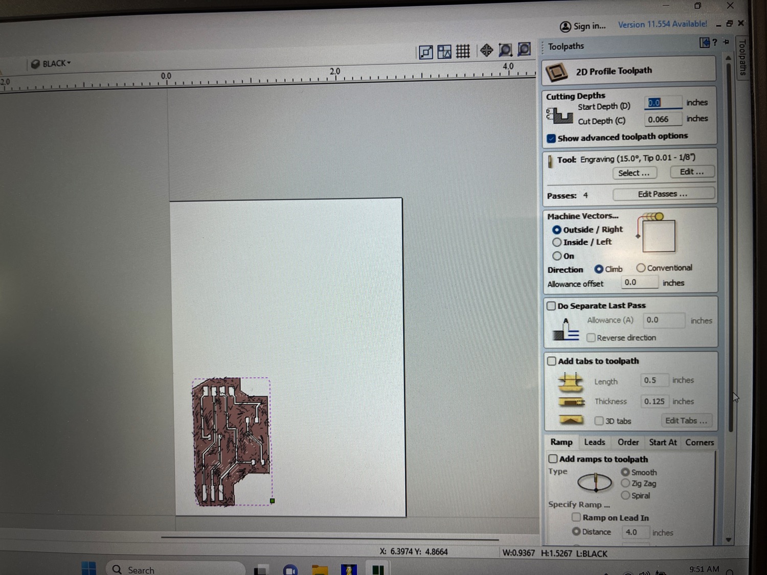
- Create a profile cut for the edge cuts. Reference the images below.
- Save file to computer. You will open this later in the Forest Scientific CNC Interface.
- Secure your PCB blank to the milling machine with double sided tape. Ensure it is level. If it is not level, you will not have a clean mill.
- Manually set X, Y, and Z homes and limits in the Forest Scientific CNC Interface.
- Load the Cut2DPro file into Forest Scientific CNC Interface.
- Double check Z height limit and levelness of the board.
- Select run/go to send the toolpaths to the machine. Watch your PCB be made!
To check depth of cut and tooling, we ran a simple test mill on our machine. Here is the result:
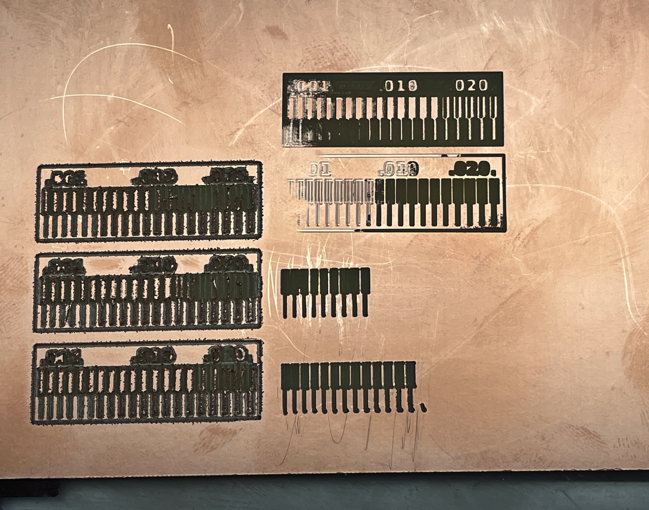
From this, you can see the whole left side of it is pretty rough... All 3 on the left were done using the 10 degree engraving bit. You can definitely make it work in a pinch but not the best. The right three tries were all done with the 1/64" end mill. We use these results to adjust the thickness of our traces. Thank you to my colleague Andy for helping work through this assignment! You can find a link to his electronics production page here.
Toolpaths:
Helpful Research, Downloads, and Equiptment
This week for research I used a lot of internet sources to try to troubleshoot the Modela MDX-50 and the errors we ran into, which I will go into detail about later in this page. The internet sources I used primarily were:
- Build Electronic Circuits "PCB Design: How to Create a Printed Circuit Board From Scratch"
- Digi-Key "Everything You Need to Know About Milling PCBs
- Build Electronic Circuits "PCB Design Guidelines for Better Layout"
- Troubleshooting for Modela MDX-50 Error Codes
- Fab Lab León - Adrián Torres Documentation Website
Our Errors
We ran into many many errors this week trying to use our milling machine, the Roland Modela MDX-50. I will form a list of the error messages I remember receiving while trying to mill our first board and what they mean.
- 0000-0000 : This was an errror we received and I could not find anything about what it meant. Unknown Error.
- 1025-0000 : [Milling Data] A wrong command is detected. Solution: Check the cutting data & Check the setting on the computer.
- 1026-0000 : [Milling Data] The address is not defined. Solutions: Check the cutting data & Check the settings on the computer.
- 1027-0000 : [Milling data] The parameter is not defined. Solutions: Check the cutting data & Check the settings of the computer.
- 103B-0000 : The automatic correction is not yet finished. Solutions: Perform automatic correction.
These errors occured numerous times each time we were trying to calibrate and set the origins of the milling machine and then output a cut to the machine. The first four errors I am unable to say exactly how we got them fixed and how they went away. The last error, error code 103B-0000 I fixed by placing the detection pin in slot 6 in the tool bar within the machine. I then ran the automatic correction and it worked (relatively) after that.
Once we got to running a test mill of our board, that is when we ran into another problem. We were finding that our spacer underneath our board, as well as the boards we have themselves, are ever so slightly not level. The cut depth of the machine is only a few thousands of an inch, so any degree off from level will make a huge difference. This made it very difficult to calibrate the z origin point.
Another issue we ran into while trying to mill- we broke the milling tool bit! Not good if you need to produce something for class, so we got another one and were trying to use it to mill. Tragedy struck again yesterday as we had just sort of figured out a way we could test our mill again when the SECOND bit also broke. We had bad luck this week. A new bit is on the way.
A long time has since passed, and we have no longer tried to mill with our Modela. We have switched to the ForestCNC ATC CNC machine. It has given us positive results and is fairly consistent in its performance.
Individual Assignment
Trial 1
Our assignment this week was: make and test the development board that you designed to interact and communicate with an embedded microcontroller.
To get started with production of my PCB, I first designed my PCB schematic in Kicad. I explain this process more during my week 6 assignment. Details can be found here. I created a very simple design for my circuit previously, which includes my Seeed Studio XIAO RP2040 microcontroller embedded in with one resistor and one LED.
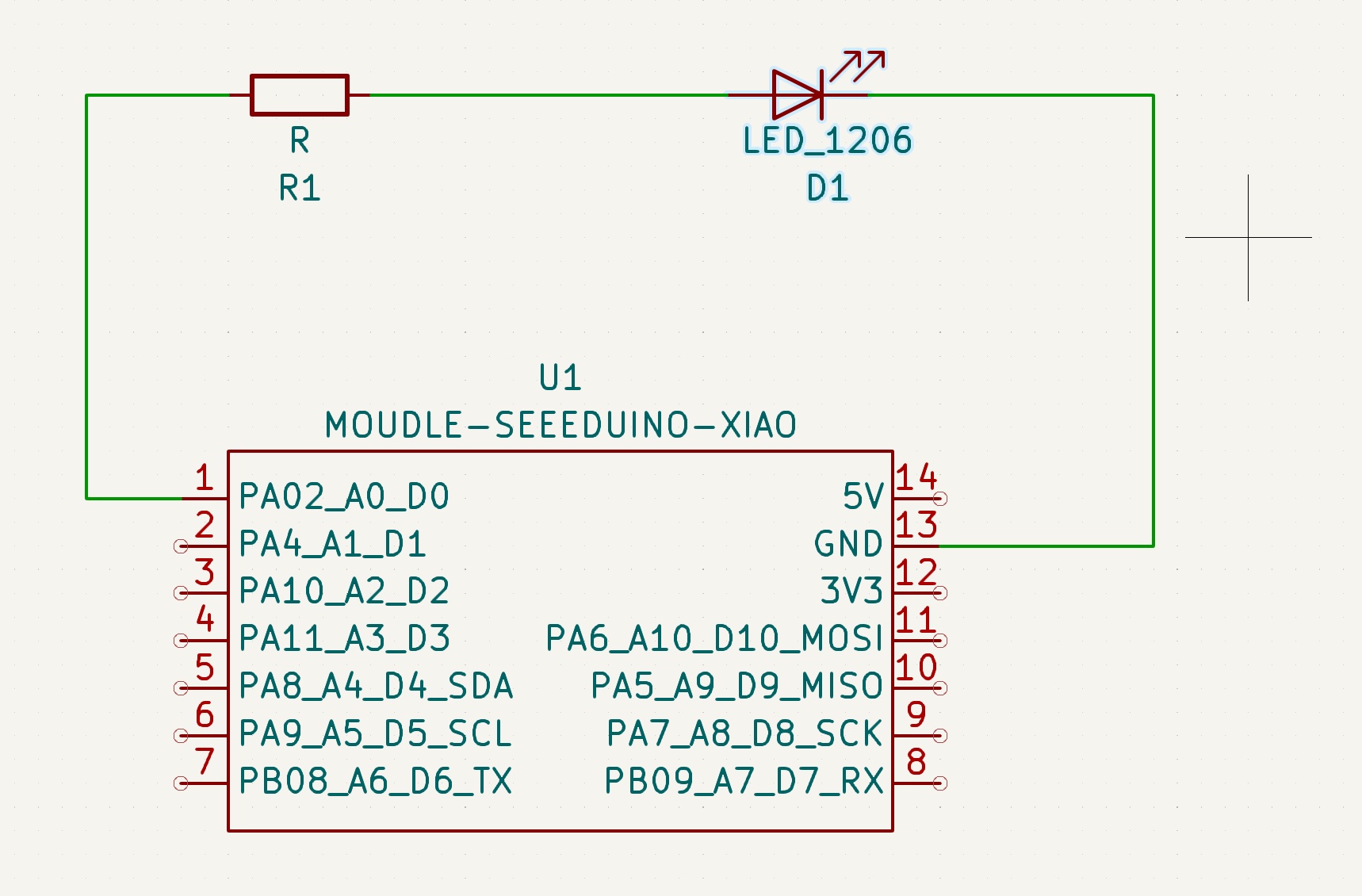
The above image is the schematic I designed. Like I said before, very simple. I have no experience prior to this class in electronics at all, and it is a challenge trying to learn how to do this in less than a week. I opted to go for the simple design for that reason (I am still learning what each component is, what is does, and how I can use it for my projects). Once I designed the PCB, I opened my design in the PCB editor of Kicad. In there, I clicked file, then plot. I followed the direction from PCB Way's Webpage and this helped my generate the Gerber file for my PCB.
This gerber file can be used in FlatCAM to generate a toolpath for the milling machine. Some modifications were needed as we tried to complete the next steps, and this is where we ran into all of the errors and issues - our milling machine.
Summary of the Week
This week was incredibly busy, as both Andy and Nikki were out of town for work until Monday, and when we tried, it failed. Over and over. Designing the PCB, no problem at all. It was the milling where all of our issues started to show. Our mill, boards, or supporting block are not level. The very slight difference in height makes a large difference when trying to mill a PCB board because we are atching away the smallest bit, and if it is off, it will not mill at all. I will include pictures below of how the test runs worked out.
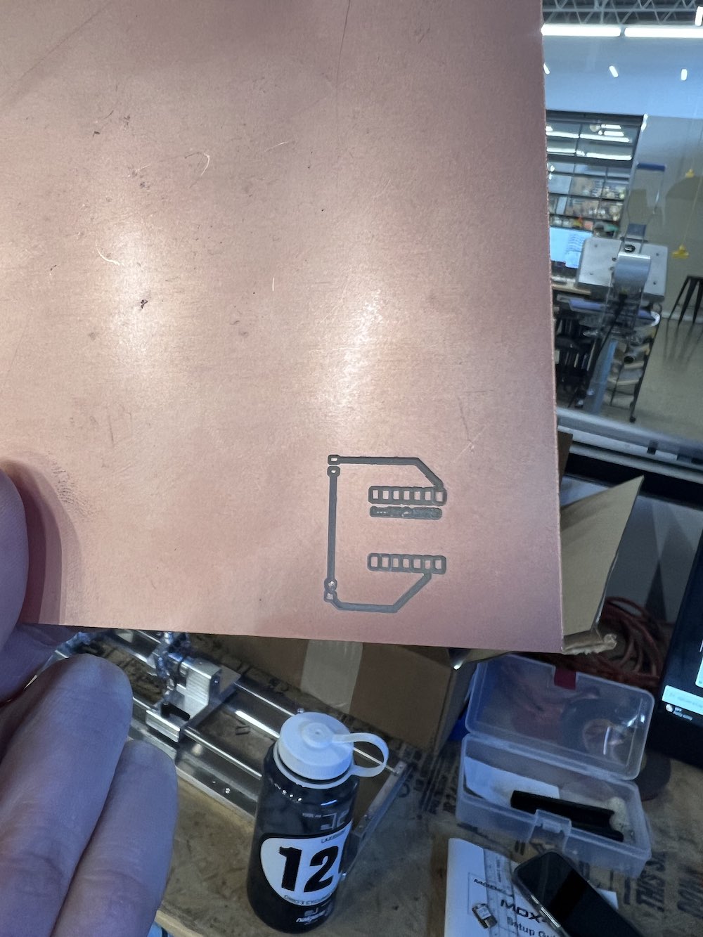
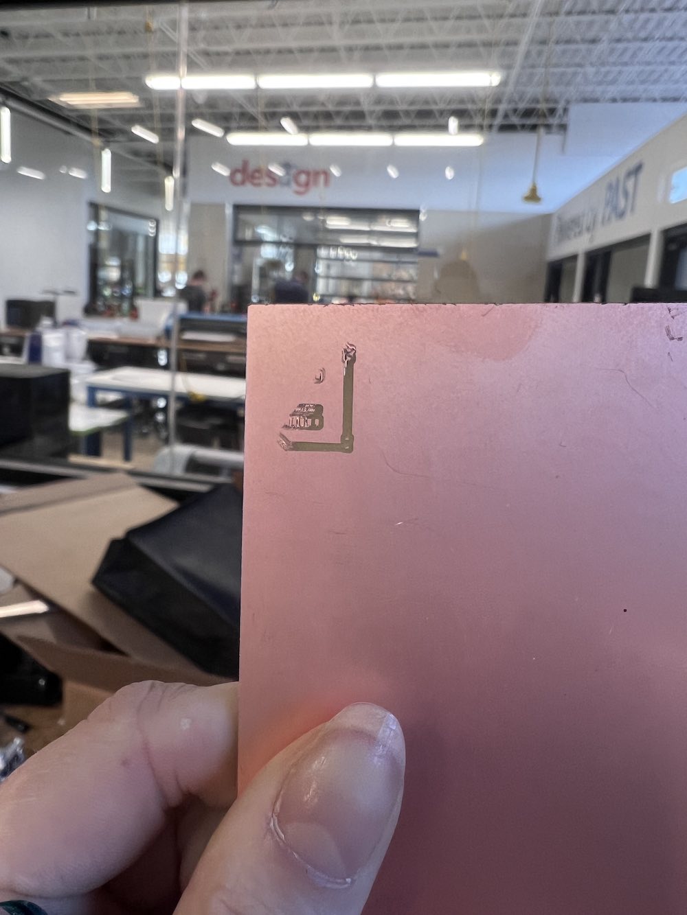
This was the first test we did of milling, and it wasn't terrible as you can see. However, it was way way way too small for our microcontroller. Andy had milled this and from here, we tried to alter the scale of the mill to fit our XIAO RP2040, which is only 20mm x 17.5 mm.
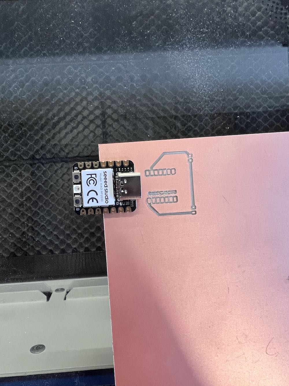
Here is where you can see that it is way too small for our microcontroller.
This one was a little messier of a milling job, and was also too small. So we tried again.
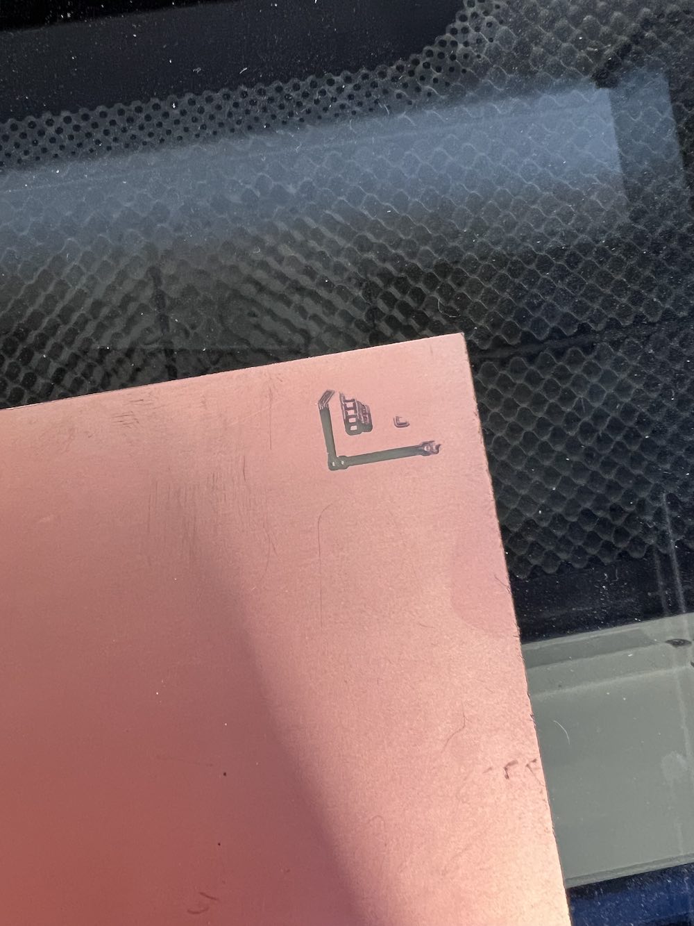
This run, we could tell more that it was not level. The bit was not coming into contact with a little over half of the toolpath on the board.
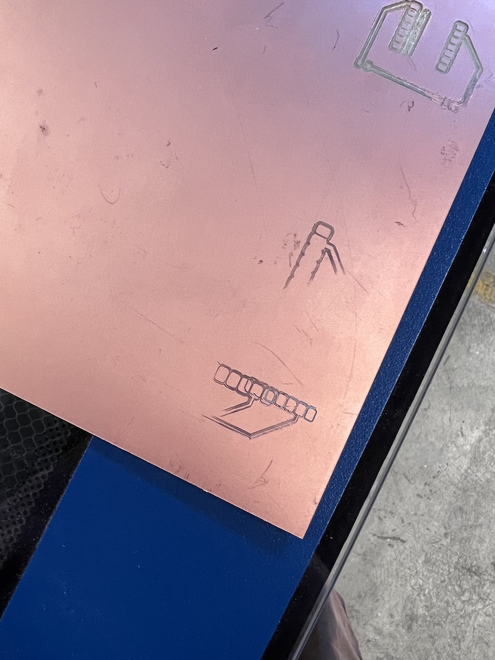
Somehow, it was getting worse with each mill.
This is when we broke the tip off the bit.
Success has finally come!
Trial 2
Well.. I have come back around to this page (I originally did this for week 8 and it is now week 13) and finally have good news I can add to it. We have successfully milled, soldered a successfull PCB and it has the proper connections we need. I will go into detail about how we milled our PCB with the Forest CNC Machine.
Kicad
As it was before, so it shall be again. I started again in Kicad, this time following the design from the fabXIAO page from Adrian Torres. Using Kicad to create a schematic, I added all my components (following my week 6 directions), added the tracks, then added all the components to the PCB viewer and editor. Once in the PCB editor, I rearranged my components and added the routes that would remain between the pads. I then switched to the edge cut layer and added the lines that would be cut out and define my PCB board. I remembered from one of the previous trials that the routes were too thin to be useful in soldering my components onto my board. To fix this, I selected each route path and edited their thickness from 0.25 to 0.6. This ensures there is enough copper remaining on the board to connect my pads as needed. From the Kicad PCB editor, I selected file, and exported it as an SVG file. The application we use for the CNC machine is Flatcam. You can use this software to edit your PCB before production, but we mainly used it to push our files from our USB drives to the CNC machine; it gives the machines the toolpaths it needs in order to mill our PCB.
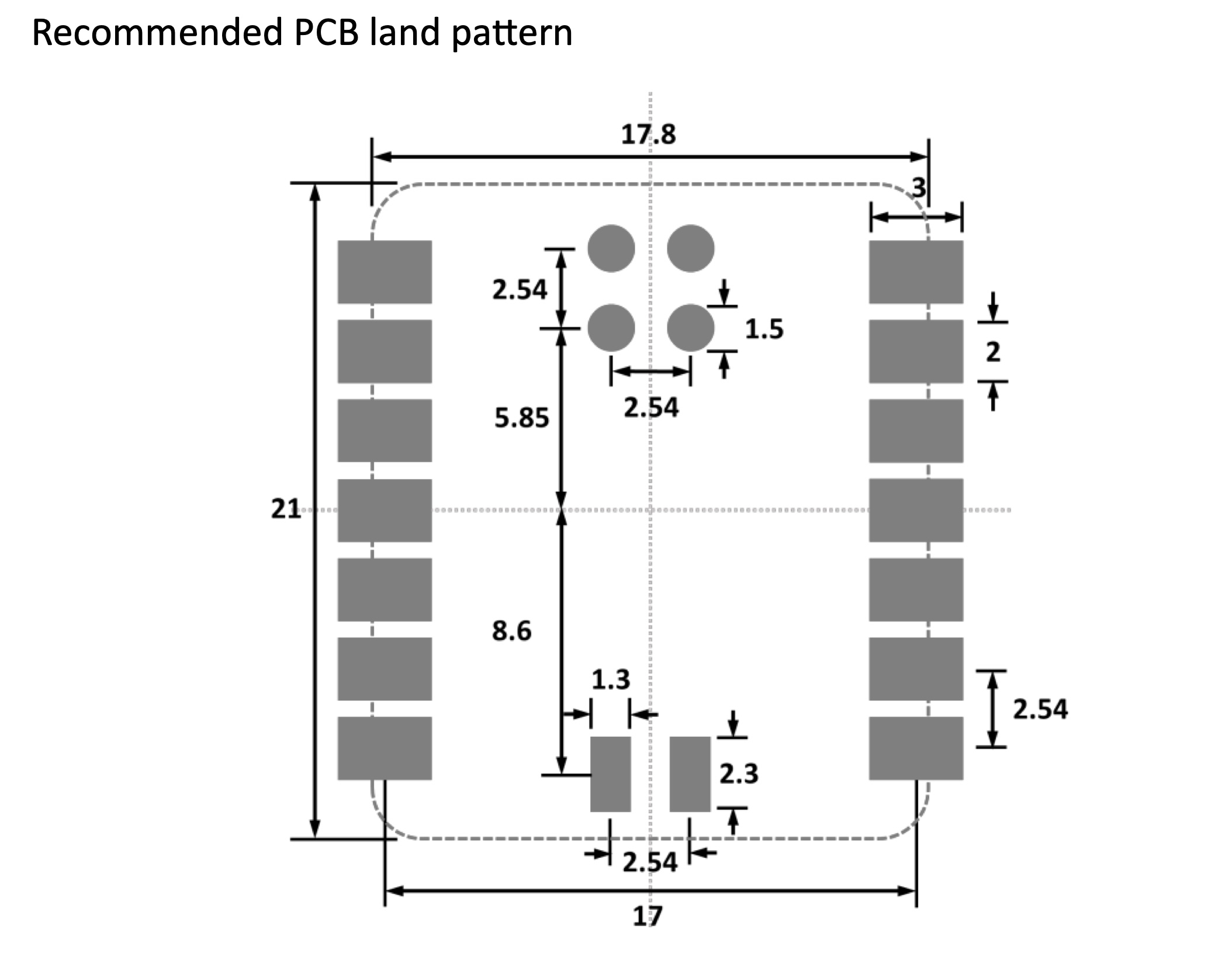
This is the recommended PCB layout and spacing for the XIAO RP2040. This helped fix the sizing issue we kept running into where our milled board was not big enough and the pads were not spaced out enough for the XIAO component to proper fit. We were not able to use the wrong-sized board.
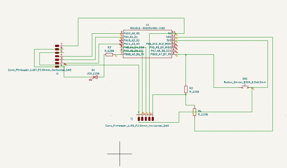
This is what my layout looked like in my schematic in Kicad when I was almost finished. You can see arrows in the image which appear different colors. The red arrows mean errors or areas that are not connected to any specific pins.
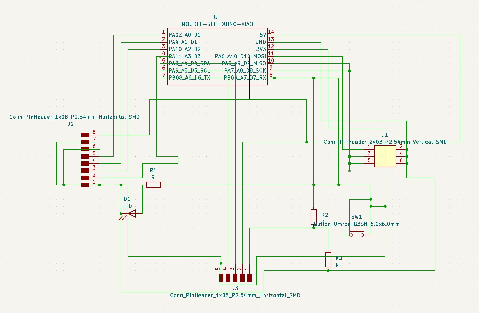
This was the final version of my schematic for this PCB. Using this, I updated the PCB editor in Kicad with the components and could move from there.
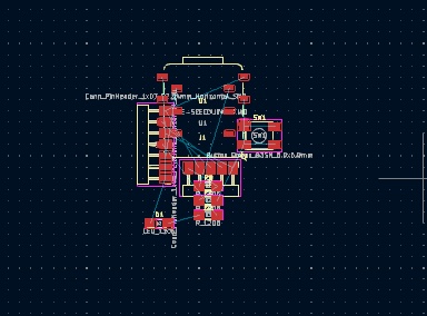
This is how the components look when they are first added to your PCB view.
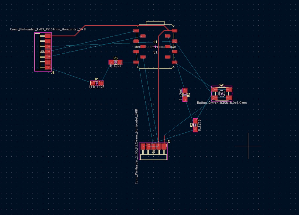
I am adding routes where the copper will remain after milling. Kicad automatically puts the traces at a thickness of 0.25. To ensure the remaining copper would be thick enough, we found 0.6 to be the best option.
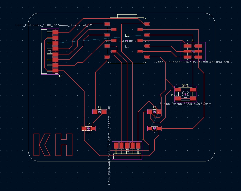
This is how the overall layout turned out. I ended up rearranging the components after my first successful mill to fit better on my board. I also added the KH in the bottom corner after I had already gotten this milled.
FOREST CNC ATC CNC:
- Model: ForestCNC ATC CNC
- Software: Vectric Cut2D Pro
- File type: DXF File from Kicad to Cut2D pro.
- Specifications: Cut2D Pro output to ForestCNC software.
- Tools: 1/64 end mill, 10 degree engraving bit, 15 degree engraving bit.
- Material: FR-1 PCB Board
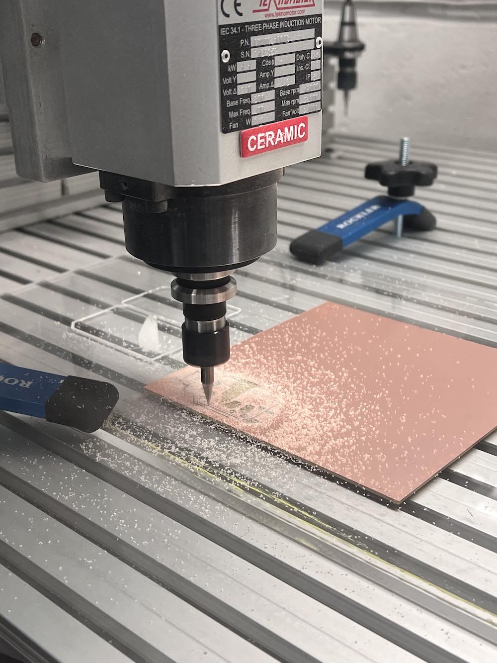
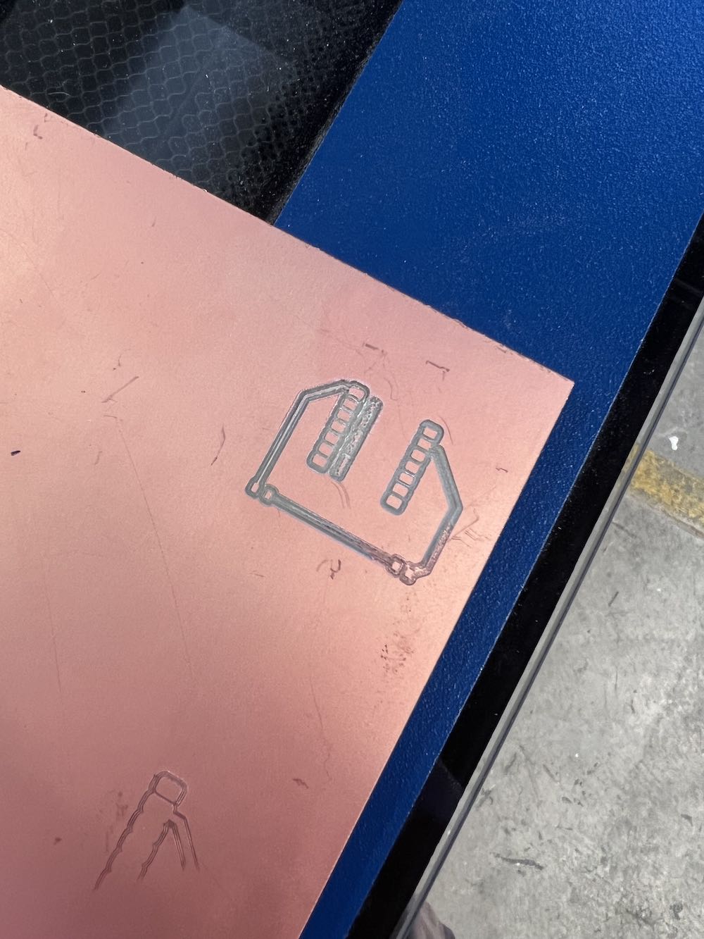
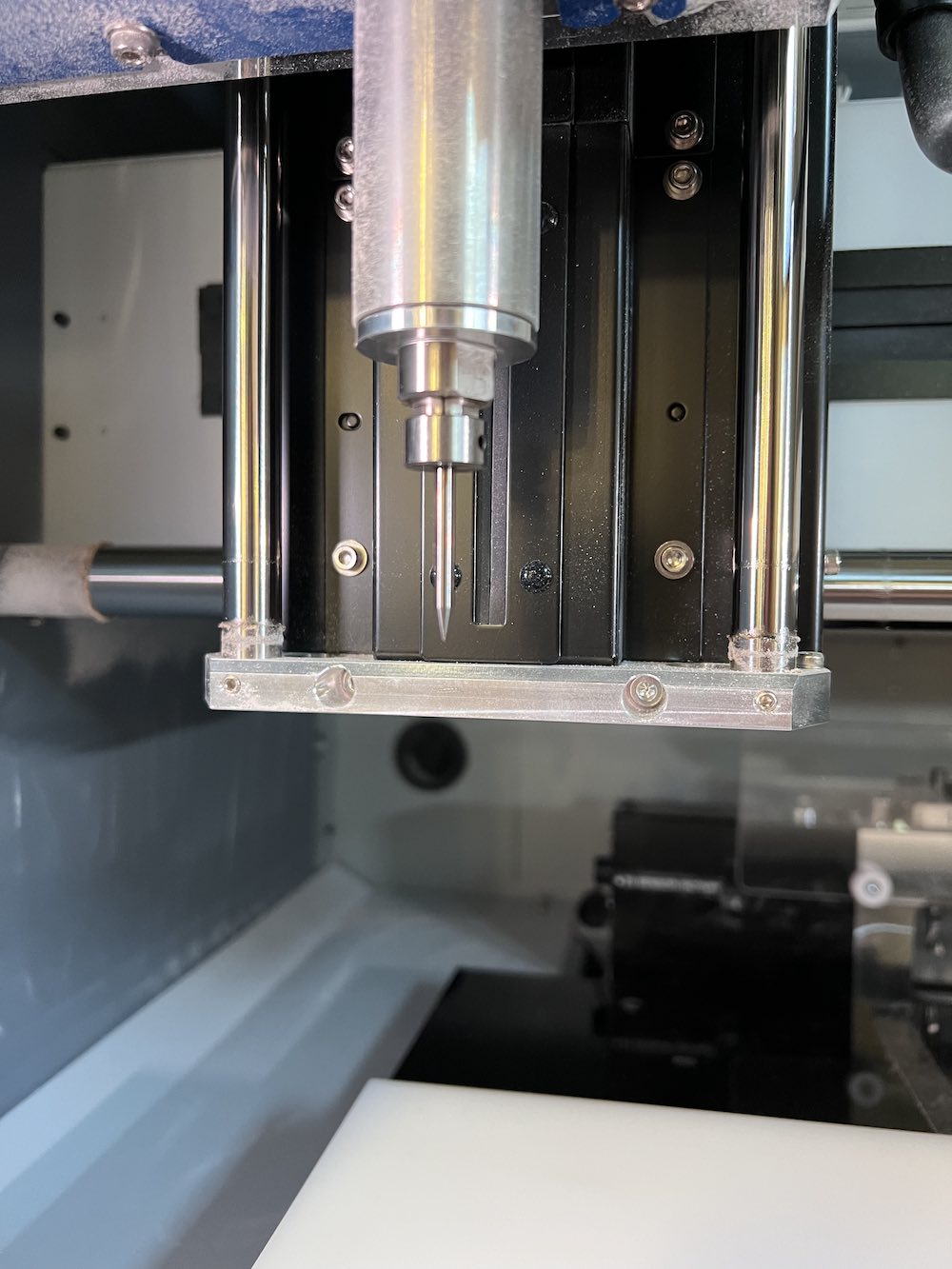
This is the Forest CNC machine hard at work milling my PCB
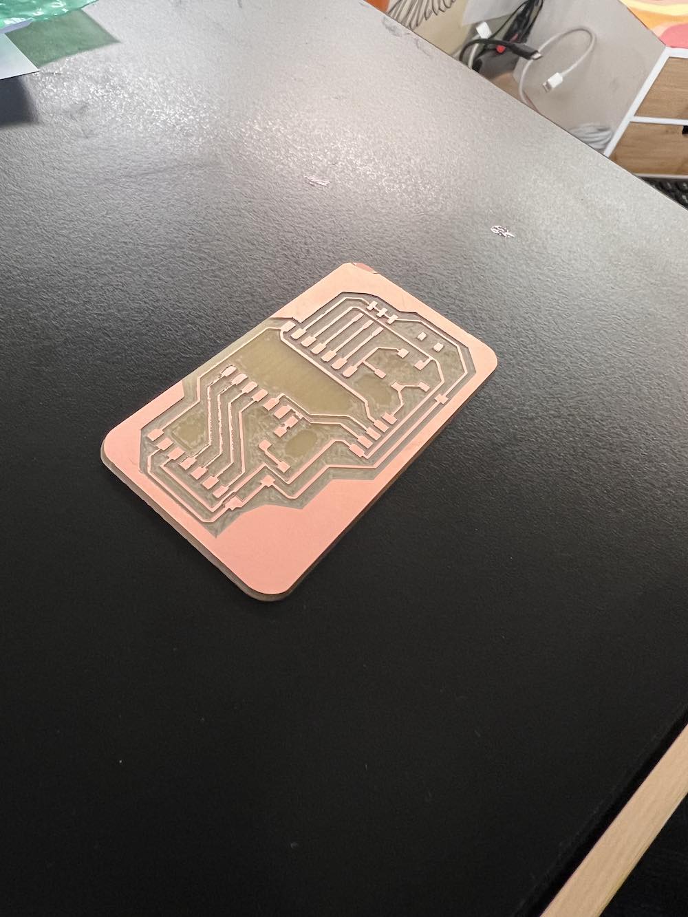
Here is how the PCB looked after it was wiped down and the dust was removed.
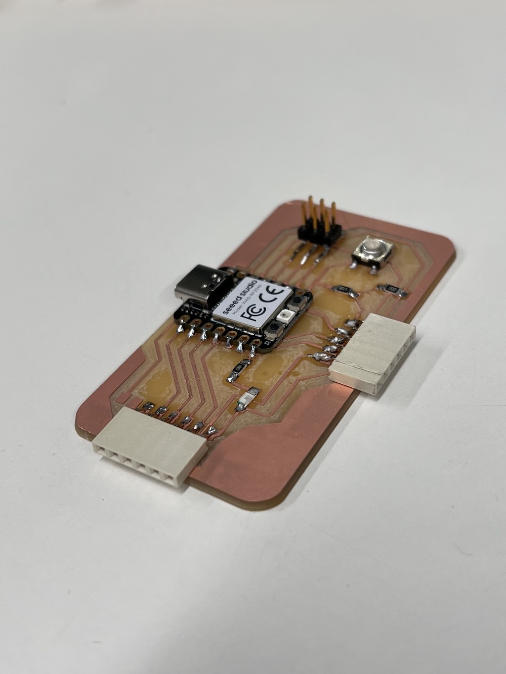

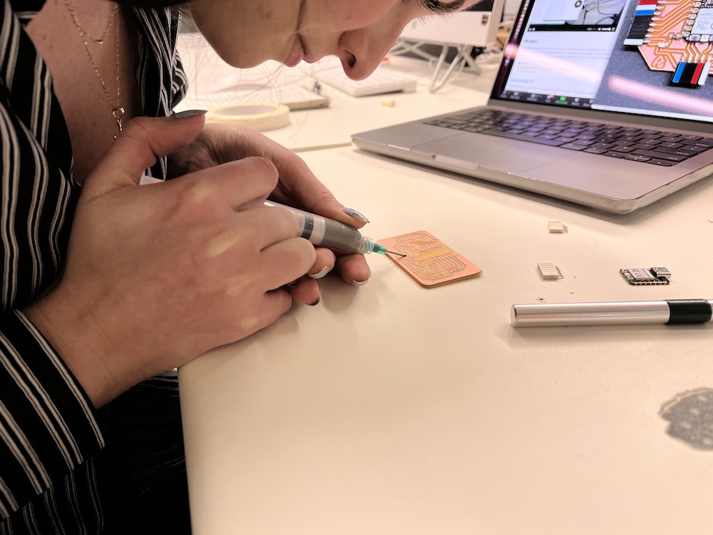
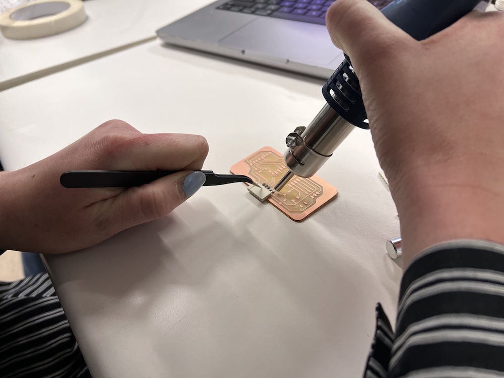
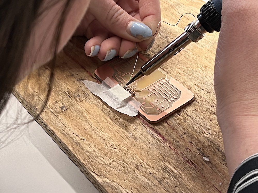
Soldering Gallery
General Steps for Milling My PCB with Forest CNC
- Design your PCB layout in Kicad and export
- Save file onto flashdrive as an SVG
- Upload SVG file into FlatCAM
- Load board into routing area and secure with double sided tape
- Send GCode to Universal GCode Sender (UGS)
- Use UGS to send code to router to be milled