6. Electronics Design
Our assignments this week are all about designing electronic boards and communicating with microcontrollers.
Group Assignment
For our group assignment, we were asked to
Our Test Equiptment
For this week, Andy, Nikki, and I have been abnormally busy with our work schedules. We are also taking this class for work and have been managing it within our 40 hour work week. Each of us has used multimeters in the past but none of us have gotten to using it this week. I will update our group and my individual page when I have time.
Update here (early November): I have gotten more time (finally) to put into Fab Academy and coming back to finish the page.
Unfortunately, here at our facility, we do not have an oscilliscope. We are working with partners to see if anyone has one we could borrow temporarily, but because we are remote students, we do not have 100% of the tools and equiptment necessary to do every single aspect of the assignments. I wish we did, but without funding specific to the materials, our inventory is not too small, but is kind of small.
We have a multimeter, which I will go into detail about below, but for the time being, we are unable to document the use of an oscilliscope.. because we don't have one. :(
Digital Multimeter
Multimeters are one of the most useful testing equiptment that I've used in electronics so far. Way back in high school we used them in our physics and engineering classes when creating and using circuits, along with other things. They have the capability to measure voltage, current, resistance, and more depending on the type and brand that you get.
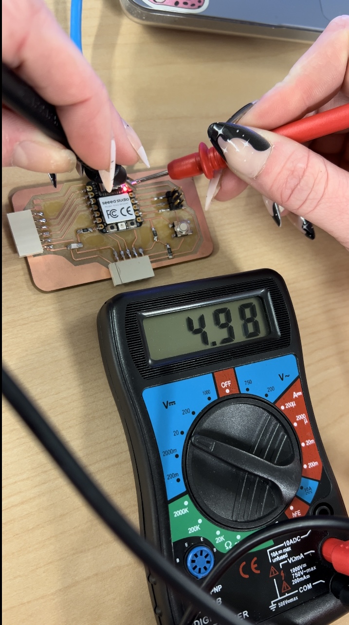
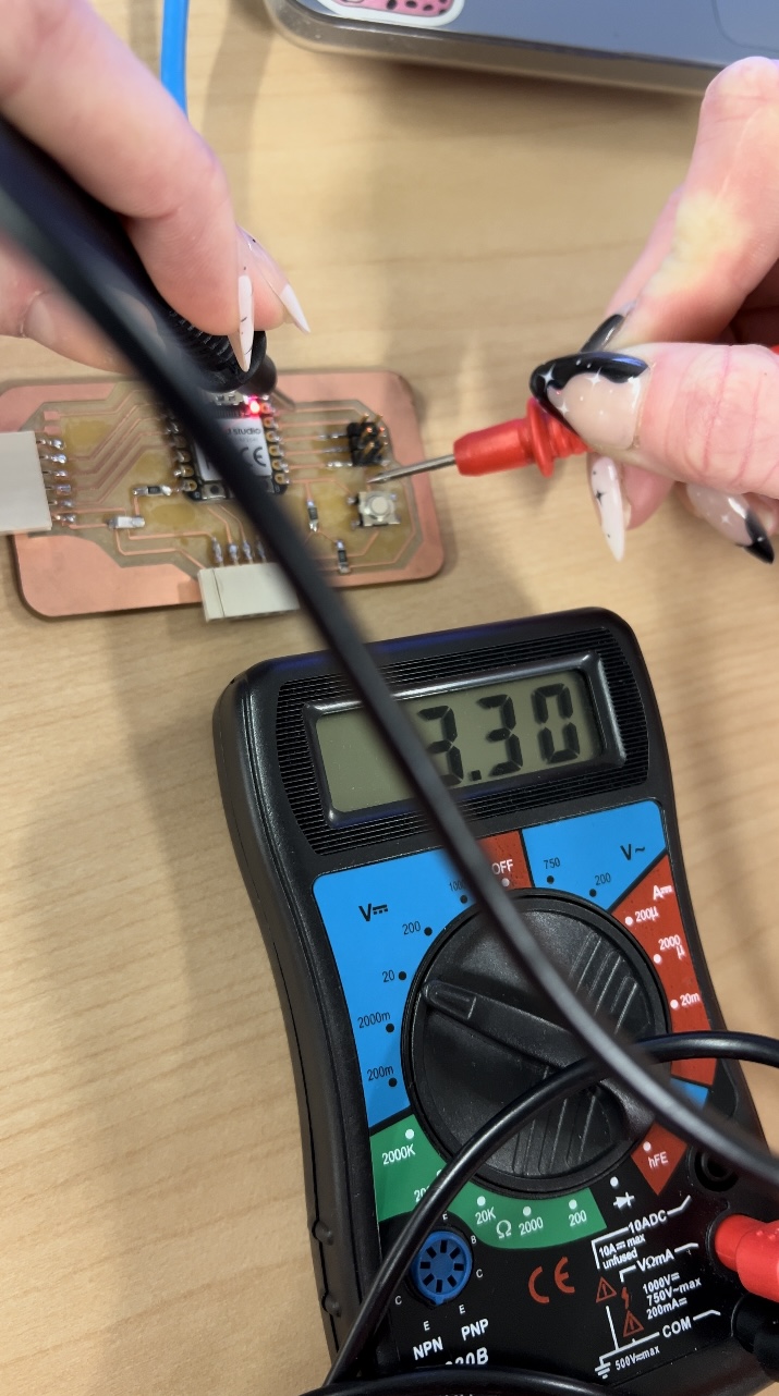
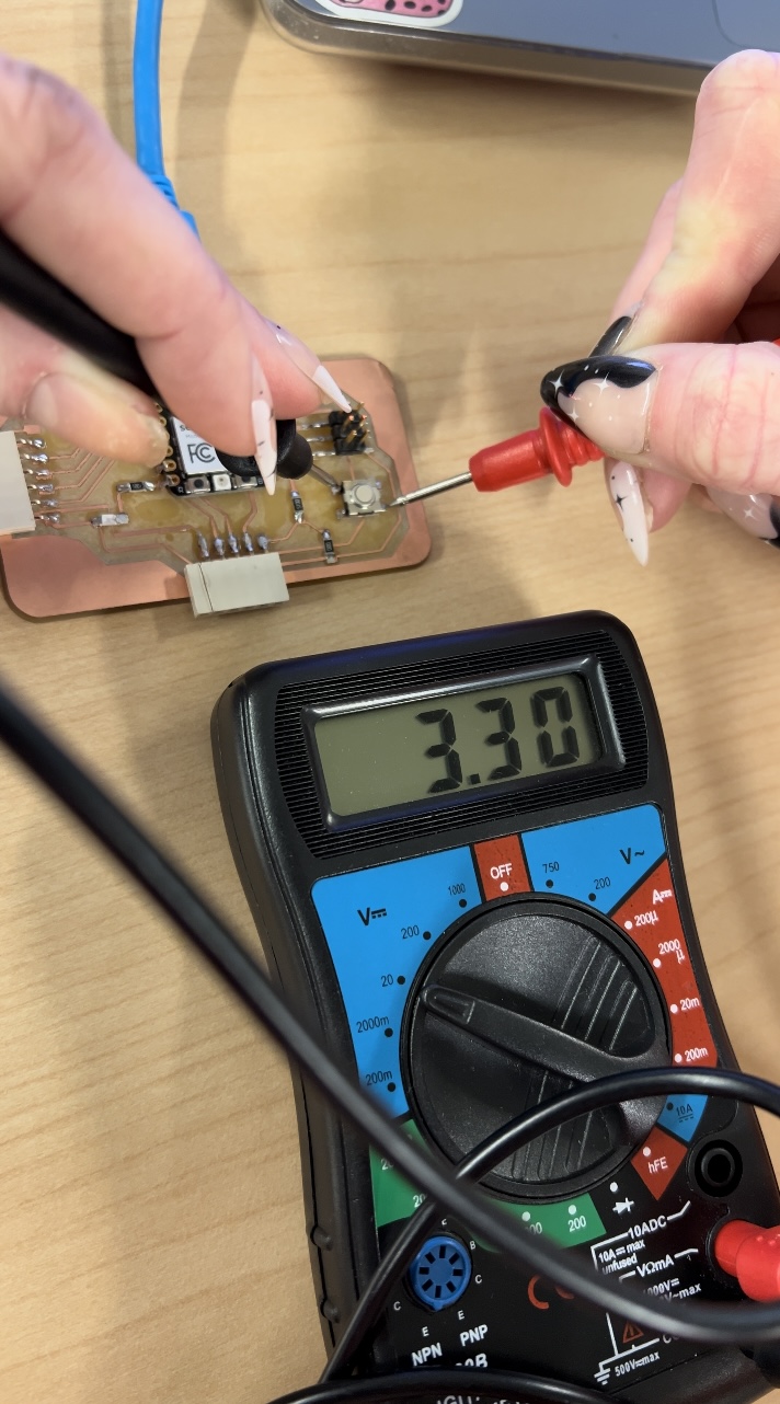
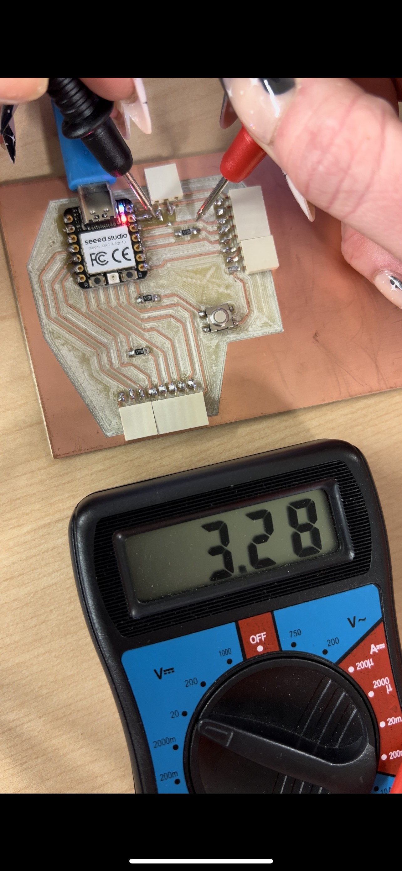
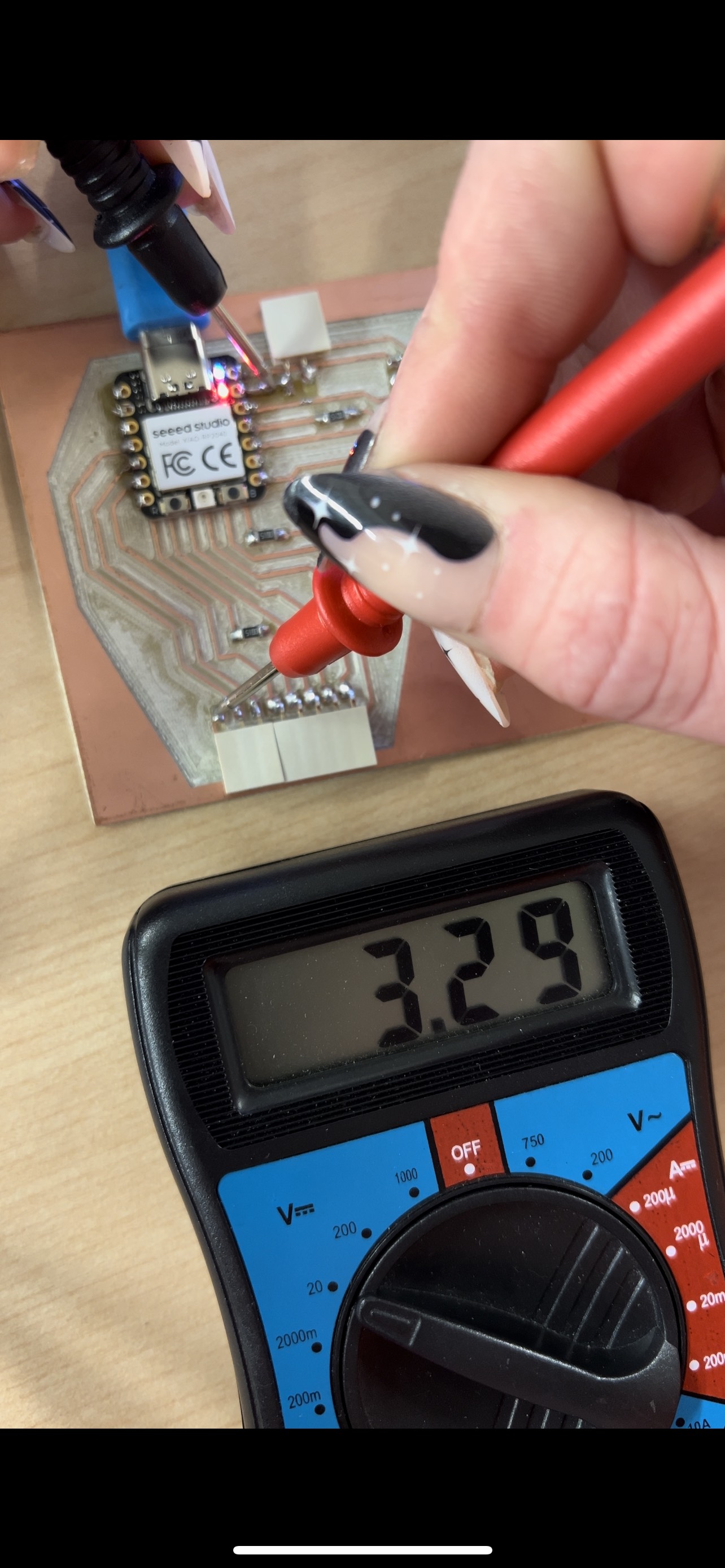
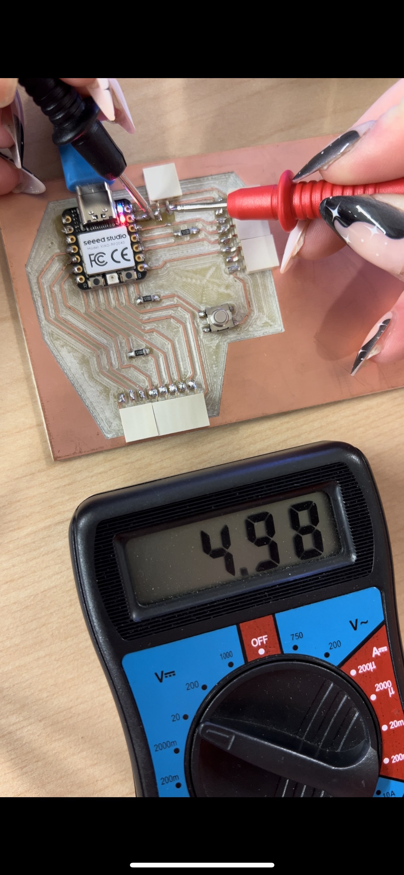
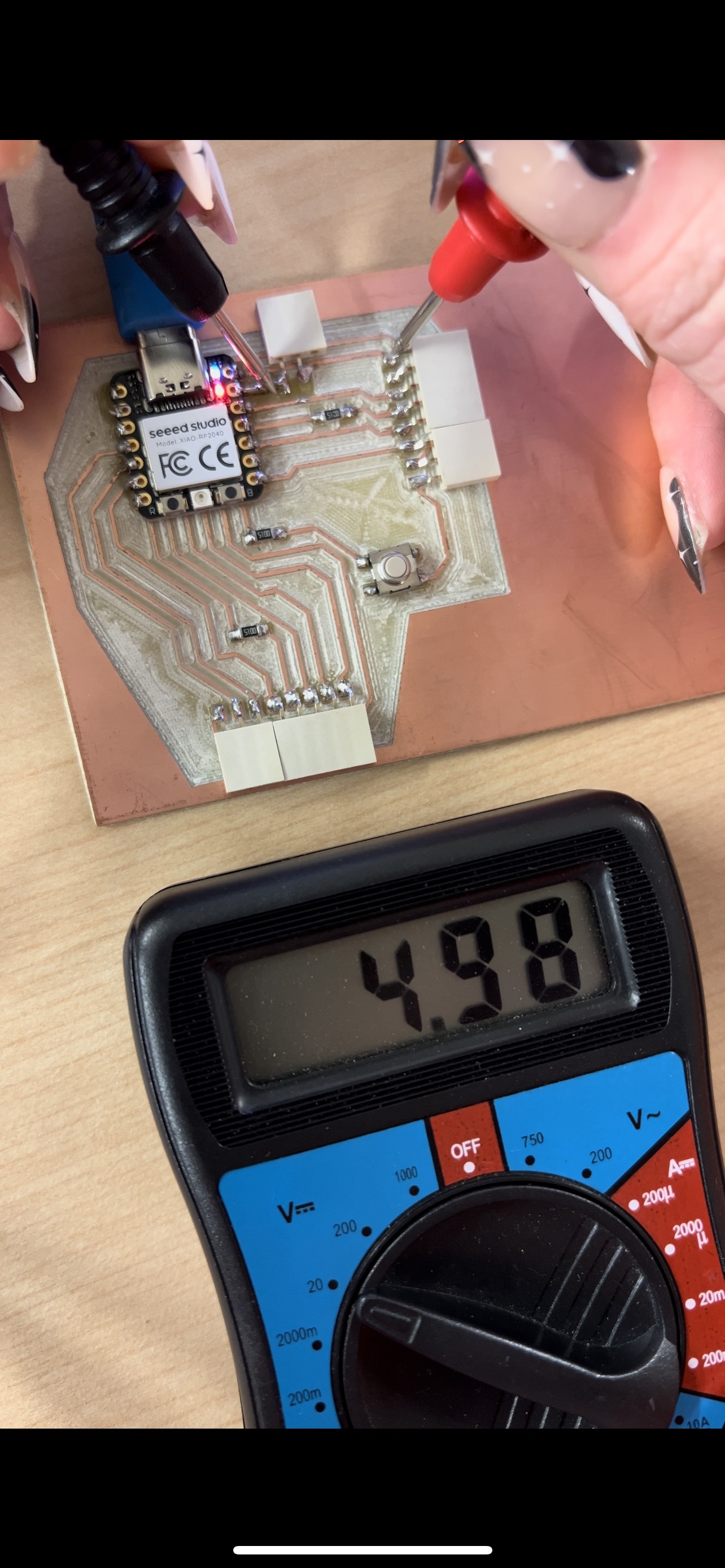
To complete this weeks assignment, we used my fabricated PCB and a multimeter. We are doing so to make sure I have adequate connections from my microcontroller to my pads and that my board will function properly.
First, we gave my board power by plugging it into the computer. This turned on the light on the XIAO RP2040 so we knew that connection was good. Next, we set up my multimeter in front of the board, so that we had enough wire to reach the points on my board we wanted to measure.
To measure, the black wire from the multimeter will connect to the ground pins. The red wire will connect to your power pins/pads. We checked the voltage coming from our 5V pin, our 3.3V pin, as well as the button we put on, and the pin headers that connect to my power pins.
You can see in the image below that the results were justttt under the expected voltage, which is good. The pins were all properly soldered and worked as they should. Success. I ended up testing a second board I made later on in the course to make sure that worked as well. I included those images too. The images are screenshots from a video, so some of them have a black bar at the top and bottom. Sorry about that.

Helpful Research, Downloads, and Equiptment
To start this week, I wanted to try to use Kicad to design my circuit board. This required me to download the application from their website. I have very little experience with electronics, especially designing them, so this week I needed quite a bit of help from my fellow colleagues working on this class with me. Andy found a YouTube video that was very helpful in beginnign the design, understanding what each symbol is, what it does, how to use it, and how to connect it all. This video also helped in finding which libraries I needed to have downloaded, how to set the footprints, view in 2D and 3D, and export the model. I downloaded Kicad, dragged it into my applications folder, and opened it up.
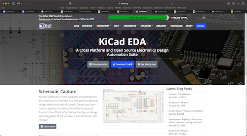
This is what it will look like when you go to the website to download the application.
This is what Kicad will look like when you open it for the first time. For what I need to do this week, I started with making a project and opening the Schematic Editor.
This is the link to the video by mathcodeprint on YouTube.
While following the video, I started with making a new project file, then opening the schematic editor. I discovered I needed to download a symbol library. Andy had followed this video prior to me starting, and sent a link to the library he needed. Kicad Symbols Library To use this, I needed to download the repository onto my computer. I saved these files into a folder on my desktop for easy finding later on. Once I had it downloaded, I opened Kicad again, went to Preferences, then manage symbol libraries. I clicked the folder icon in the bottom left of the pop up to add the files I previously downloaded onto my computer. Once I added the symbols library, I also added my footprint library by clicking on preferences, then clicking manage footprint libraries. I did the same thing as I did before for the symbols library. Once these were added I was able to follow along the video. I was able to follow along the video fully, but it was only to get my bearings about how to work in Kicad and what everything means. To start my actual project, I needed to add different symbols and footprints to match the microcontroller that I will be using.
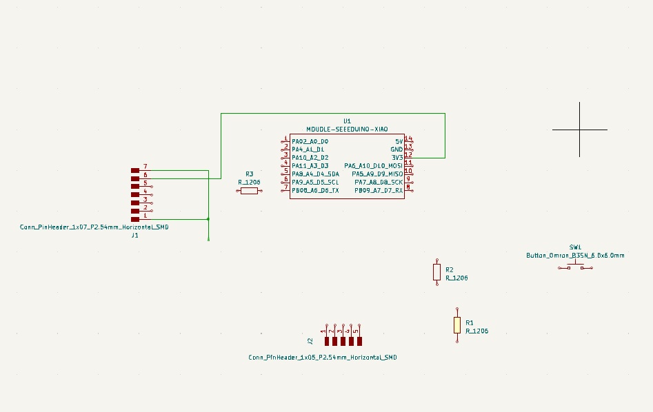
For this week, I will be using the Seeed Studio XIAO RP2040 as my microcontroller that will play into my PCB.
My PCB
This is the page to download the symbols and footprint libraries. I also downloaded the Seeed Studio library package from this webpage that I found from the Seeed Studio XIAO RP2040 page and added those to my libraries.
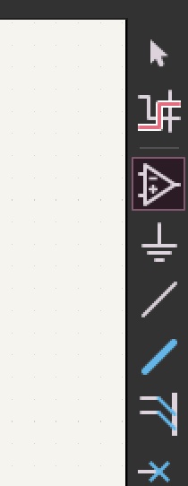
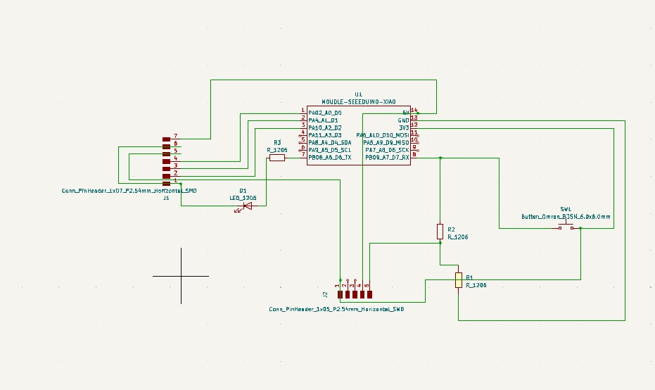
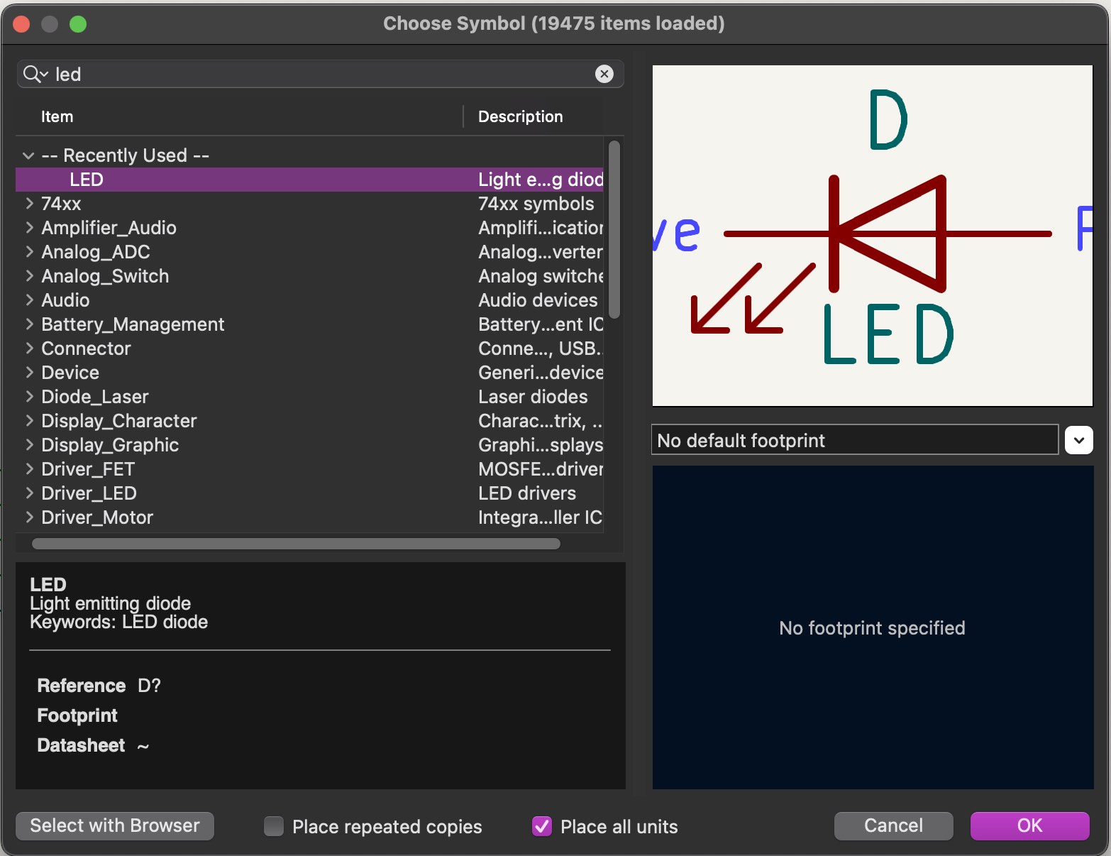
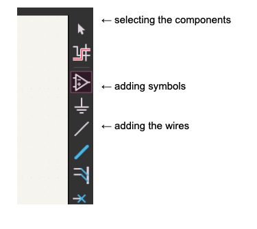
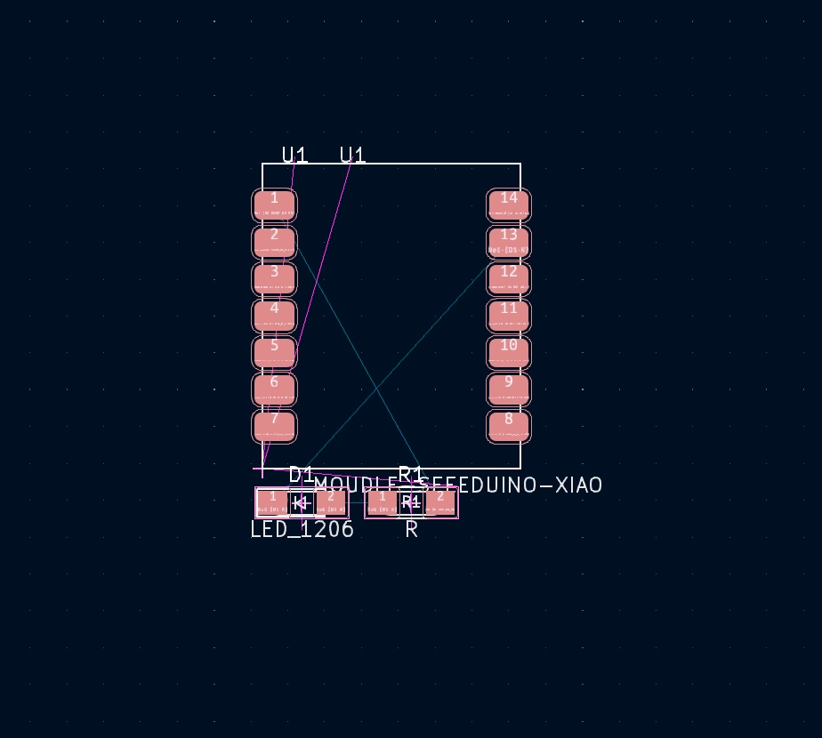
On the right side, the tools will look like this. The third from the top is how you add symbols. While following along the video, I originally clicked the add symbols button. I searched first for the LED symbol which is called Led_1206, then added that to my working field in the schematic editor.
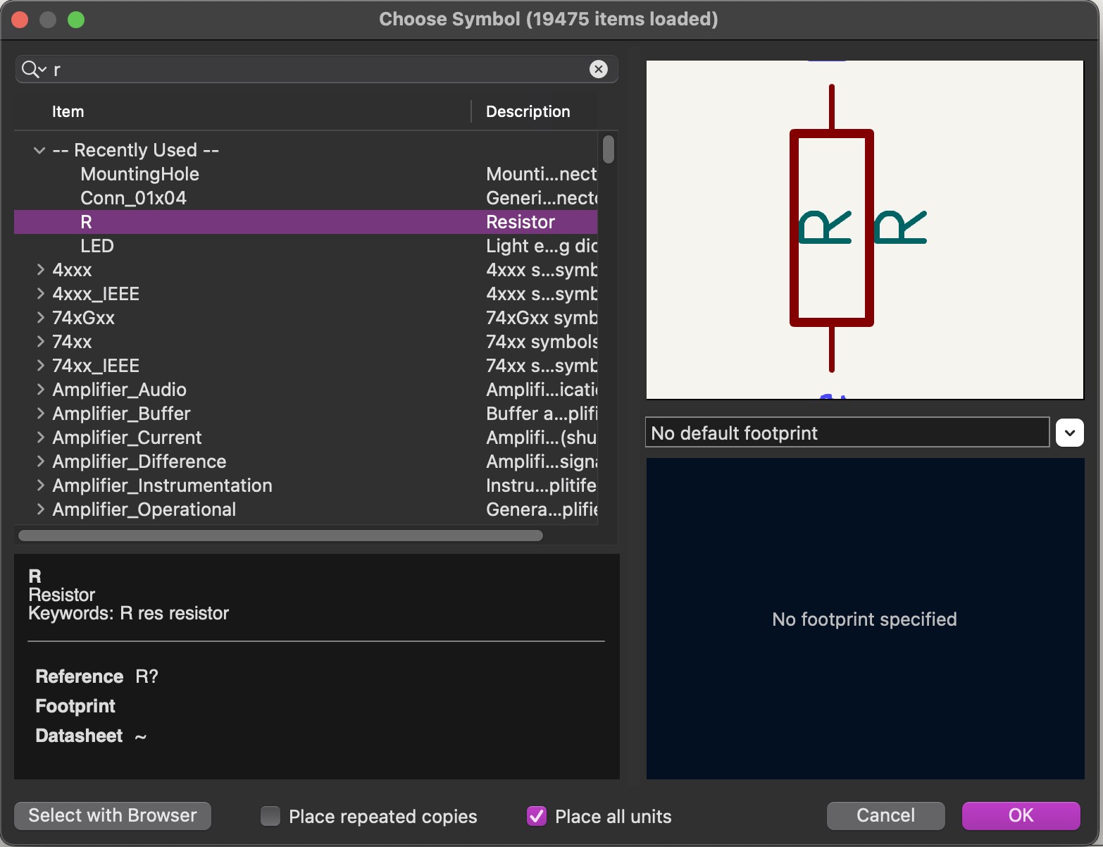
The next thing I needed to add was a resistor. I clicked the symbol adding button, then search for "R". The symbol is just called R, and I added that to my work space.
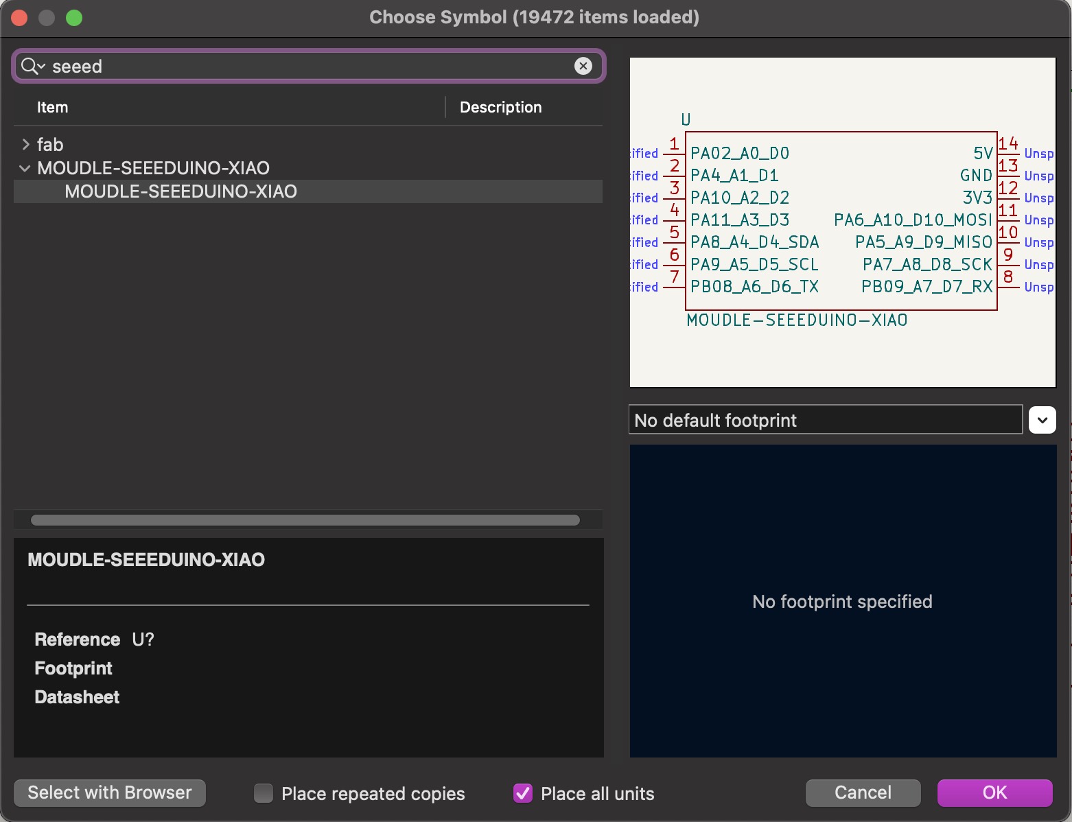
Because I am using the Seeed Studio XIAO microcontroller, this is what the symbol will look like and what it is called. I also added this to my work space.
Now that I have everything on my page, I can rearrange and connect everything.
The next step is to add wires in between to complete the circuit. To do this, I needed to connect my first pin to my resistor, which will limit the brightness of my LED after its all together. I clicked the add wires button, and drew my first connection. Then, I connected my resistor to my LED, and my LED to the GND (ground) pin on the right side of my microcontroller. This completed the full circuit.
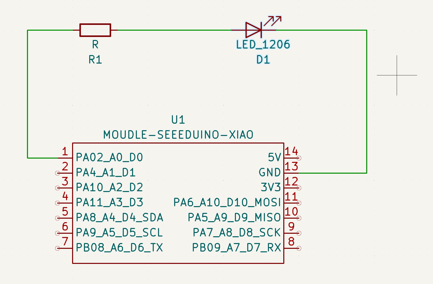
This is what it should look like.
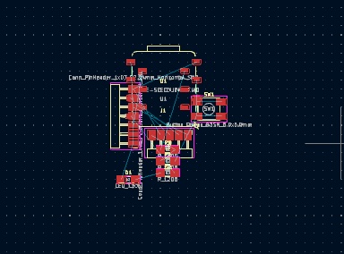
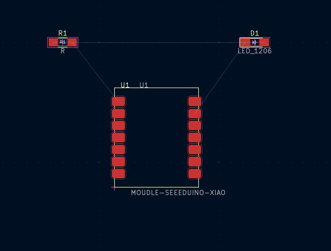
I then opened my PCB viewer. This is the green button on the top right area. It will open a new window, it should be blank. Then, push the half tan, half green button on the top that says "Update PCB with changes made from schematic (f8)". This will bring your schematic circuit into the view on PCB. You will have to rearrage the components of the board.
This is un-arranged. It would work if you connected everything with tracks properly, but it would be much more difficult to do, and to see, and to create in real time with real components. So we want to rearrange it to be more aesthetically and organizationally pleasing.
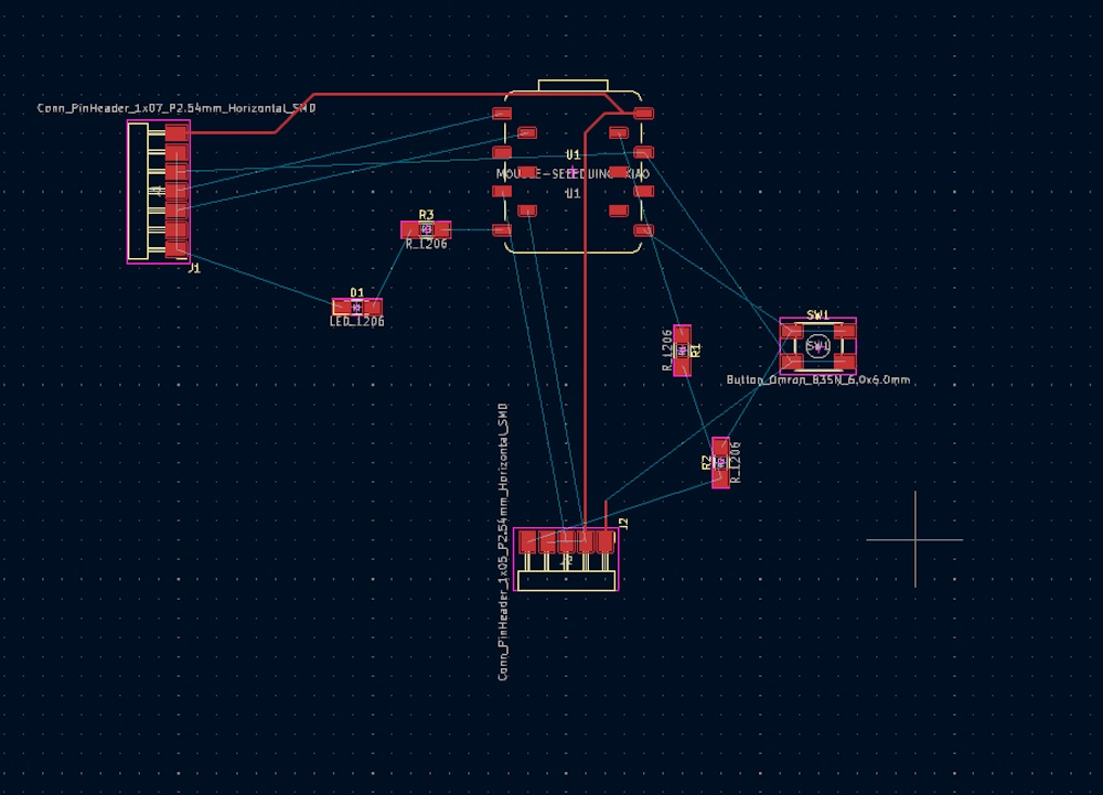
This is what it should look like after you rearrange.
Now that my components are in the PCB view, I needed to add route tracks. I did this by clicking the 4th symbol on the right side that looks like a bent line. I drew these in between each of my components to connect them. Without these tracks, you will not have any connection in the 3D view of your PCB.
I then had to add an edge cut line so when I go to the 3D viewer, it will cut my board out for me. If I do not have edge lines, I will get a very large board that goes to the end of the page, which in theory, I think, will do what it needs to, but will be too big and bulky if you try to use it in fabrication later on.
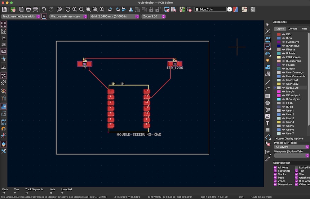
I added the cut lines by clicking on the "Edge.Cuts" layer on the right side. Then, I clicked the line button and drew a box around my components.
Once I had the edge lines on the board, I was able to open the 3D viewer by clicking view, then 3D Viewer.
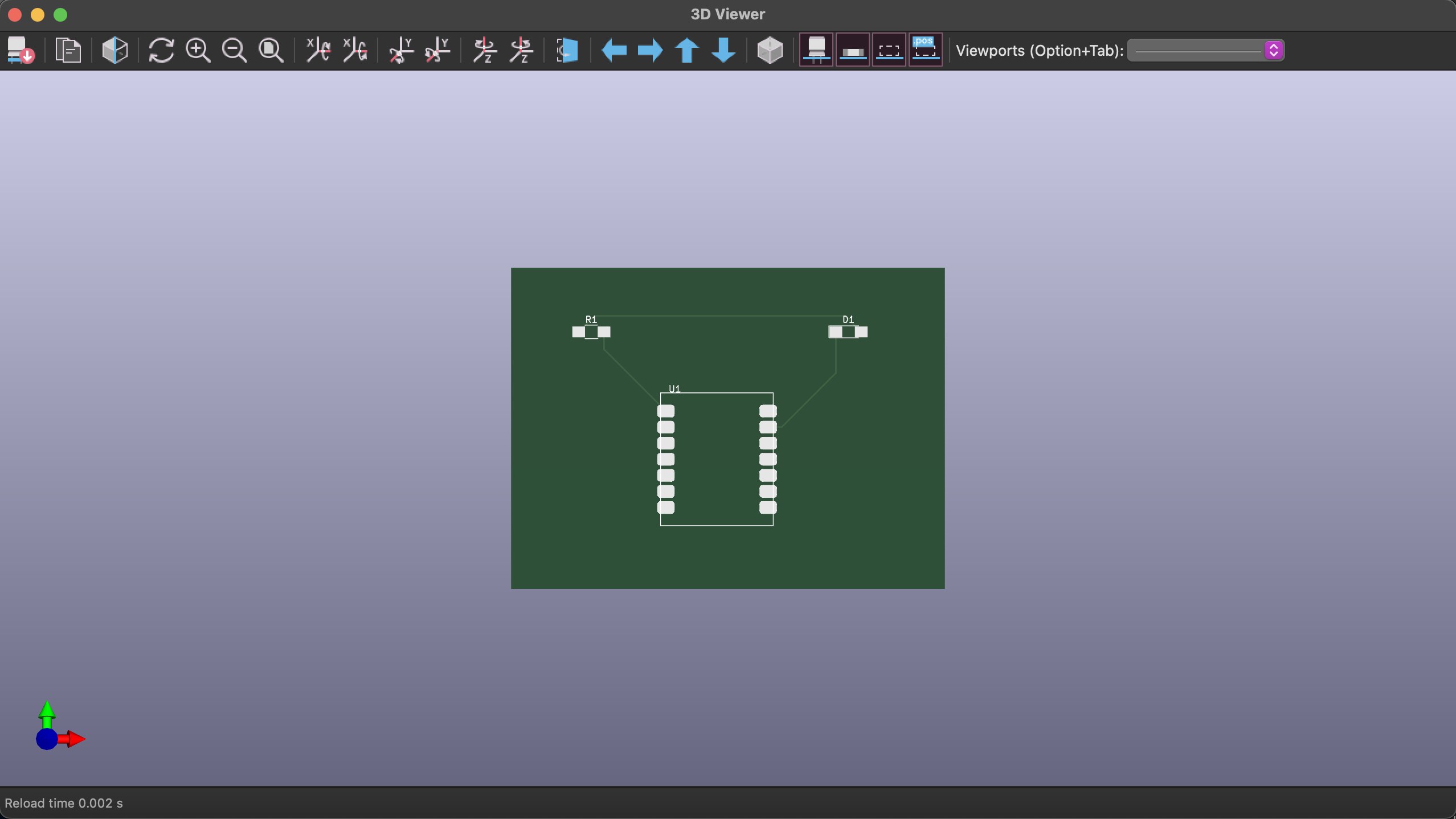
This is how mine looked once I opened the 3D Viewer.
Trying Again
I originally designed a very simple version of a pcb as you have seen above. When our lab got to the electronics production week, we ended up using a design from the Fab XIAO website. Adrian Torres has great documentation on how to create the file and how to use it in programming and the input/output weeks. Because we are all new in the electronics realm, we decided to create a replica board from his webpage to use as testers to make sure all of our equiptment and components work. For our final projects, we all plan to redesign a board and use it for our specific functions we need.