7. Electronics design
Link to group assignment page.
Update: During week 9, I have found a missing connection in the schematic file and thus had to fix that, mill a new board, and solder the components once again. The missing connection was the RST was not connected to the Reset pin on the ATtiny44. So, if reffering to my sketches, make sure to read the full documentation :)
Individual Assignment: redraw one of the echo hello-world boards or something equivalent, add (at least) a button and LED (with current-limiting resistor) or equivalent input and output, check the design rules, make it, test it.
Setting up Eagle
To design the circuit, I decided to use the Eagle application by Autodesk; I installed it off of this link. Then, I had to install the Fab library that has all the components available at the lab.
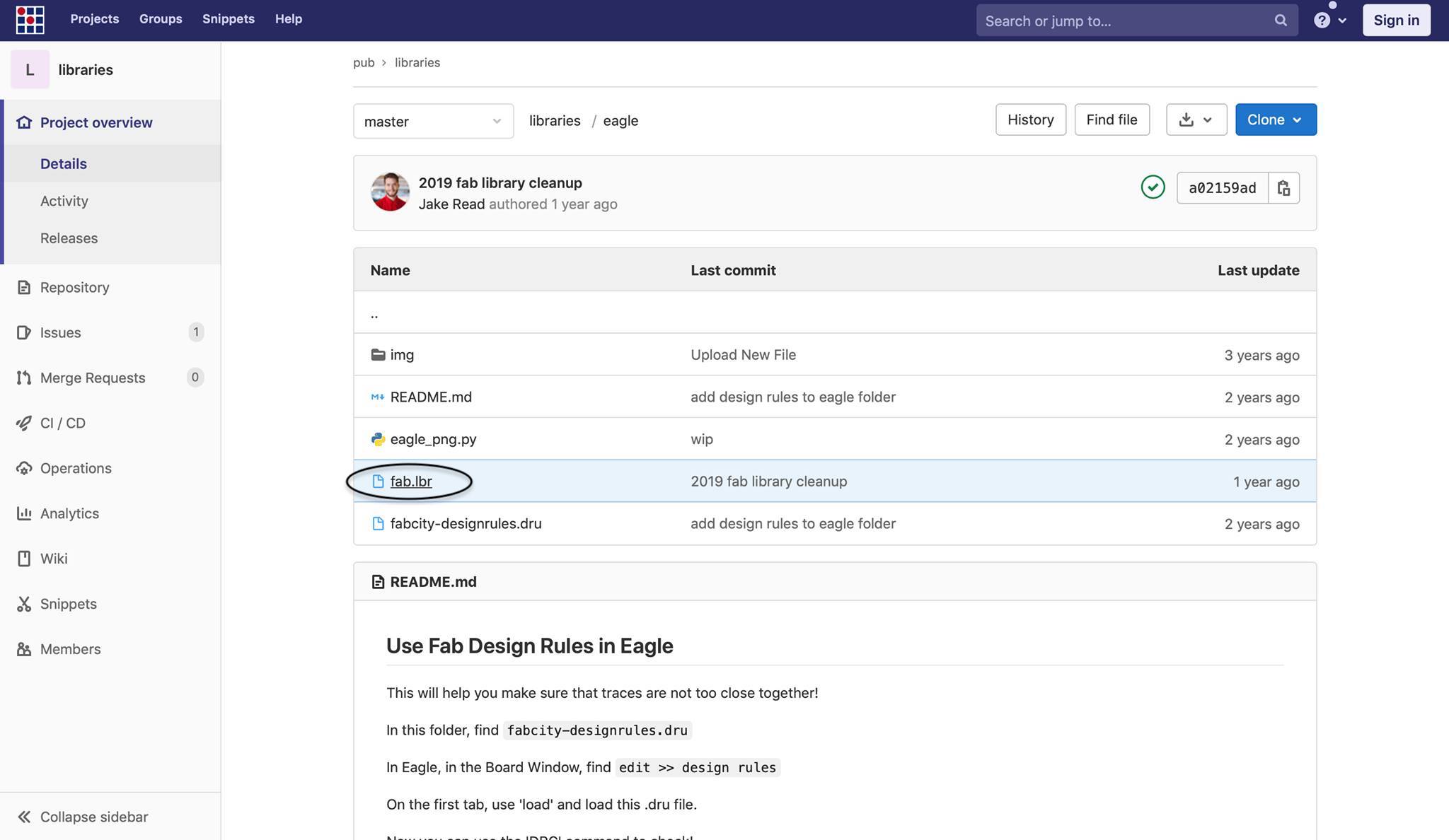
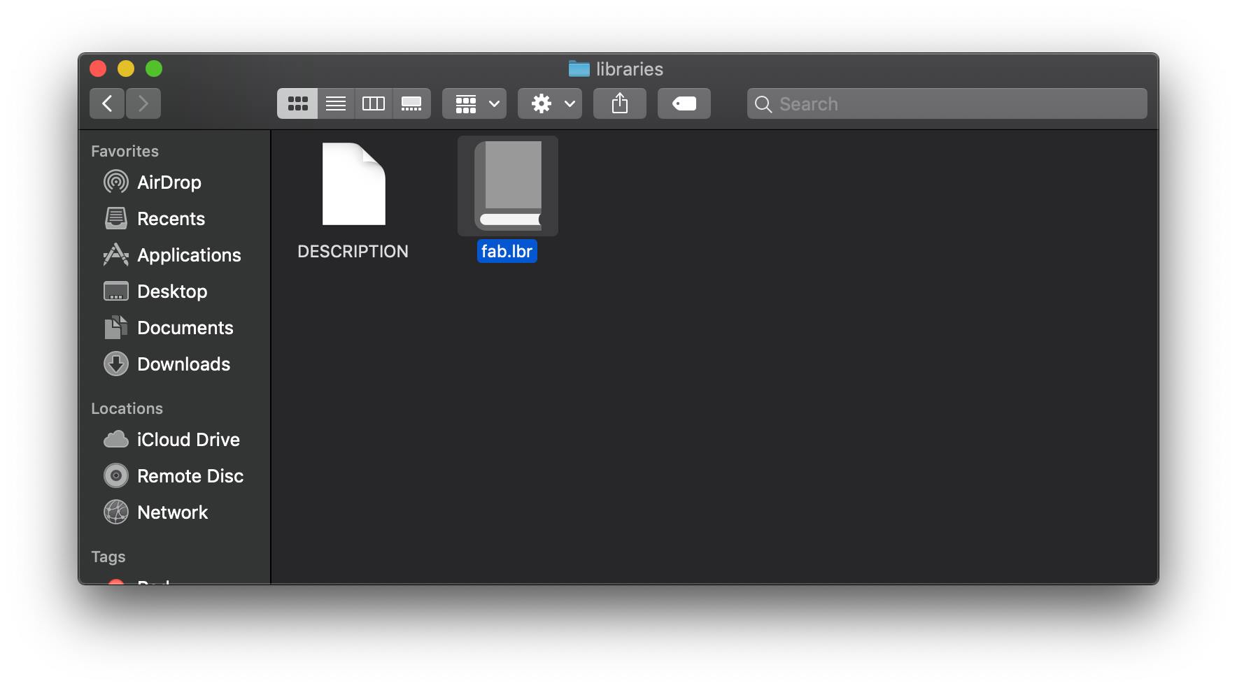
The first step to install the library onto Eagle, is to open the eagle folder, and then downloaded the fab.lbr file.
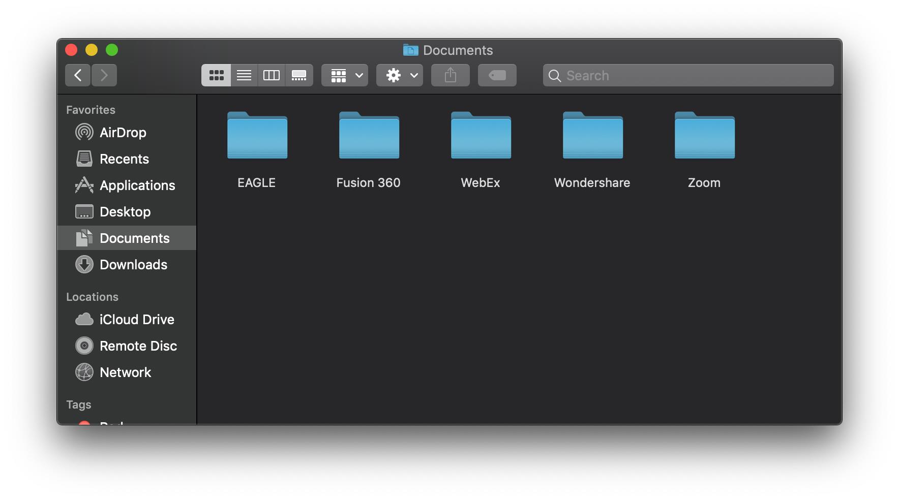
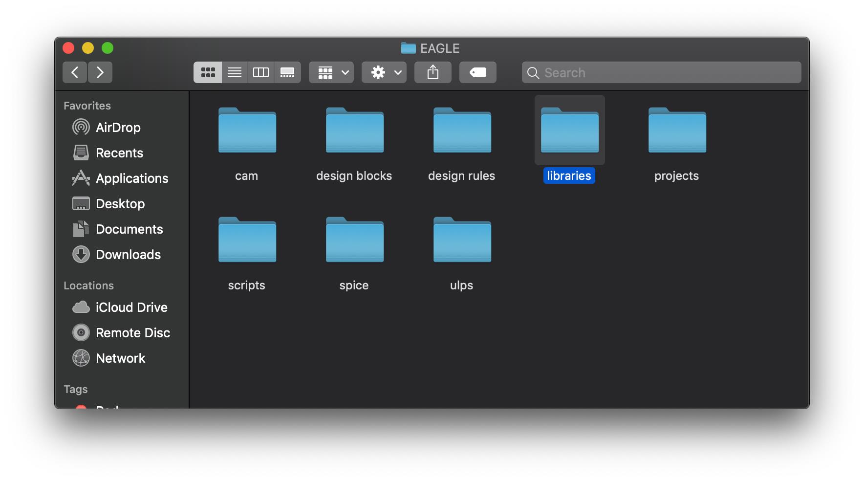
Next, I opened the Documents folder, navigated into Eagle, and finally opened the libraries folder and moved the eagle_fab.lbr into it.
ATtiny44
Starting the schematic
I launched Eagle, and then created a new project simply by New Project > New > Schematic.
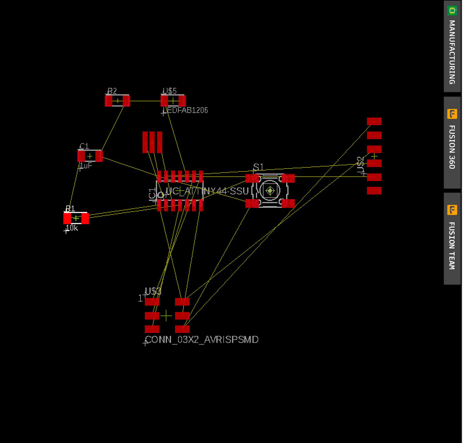
For my echo hello-world board, I decided to redraw the Attiny44 board. I started by adding the components to the schematic file (using the add part tool), starting with the Attiny44.
Below is a table with all the components and how they were connected to my board:
| Component | Connection |
|---|---|
| Attiny44 | |
| 10k Resistor | Connect a resistor to the RST and VCC pin on the Attiny44 using the net tool. |
| 499 Resistor | Connect a resistor to the LED and GND pins using the net tool as well. |
| Unpolarized Capacitor | Add an unpolarized capacitor to the VCC and GND 0f the Attiny44. |
| LEDFAB1206 | Connect the LED to the 499 ohms resistor. |
| CONN_03X2_AVRISPSMD | Add an AVRISP SMD Microcontroller to the project and start connecting it to the respective pins on your Attiny44. |
| Button | Connect the button to the GND and name a pin “BTN” for button. |
| XTAL_Resonator | Connect the resonator to the respective pins on the Attiny44. |
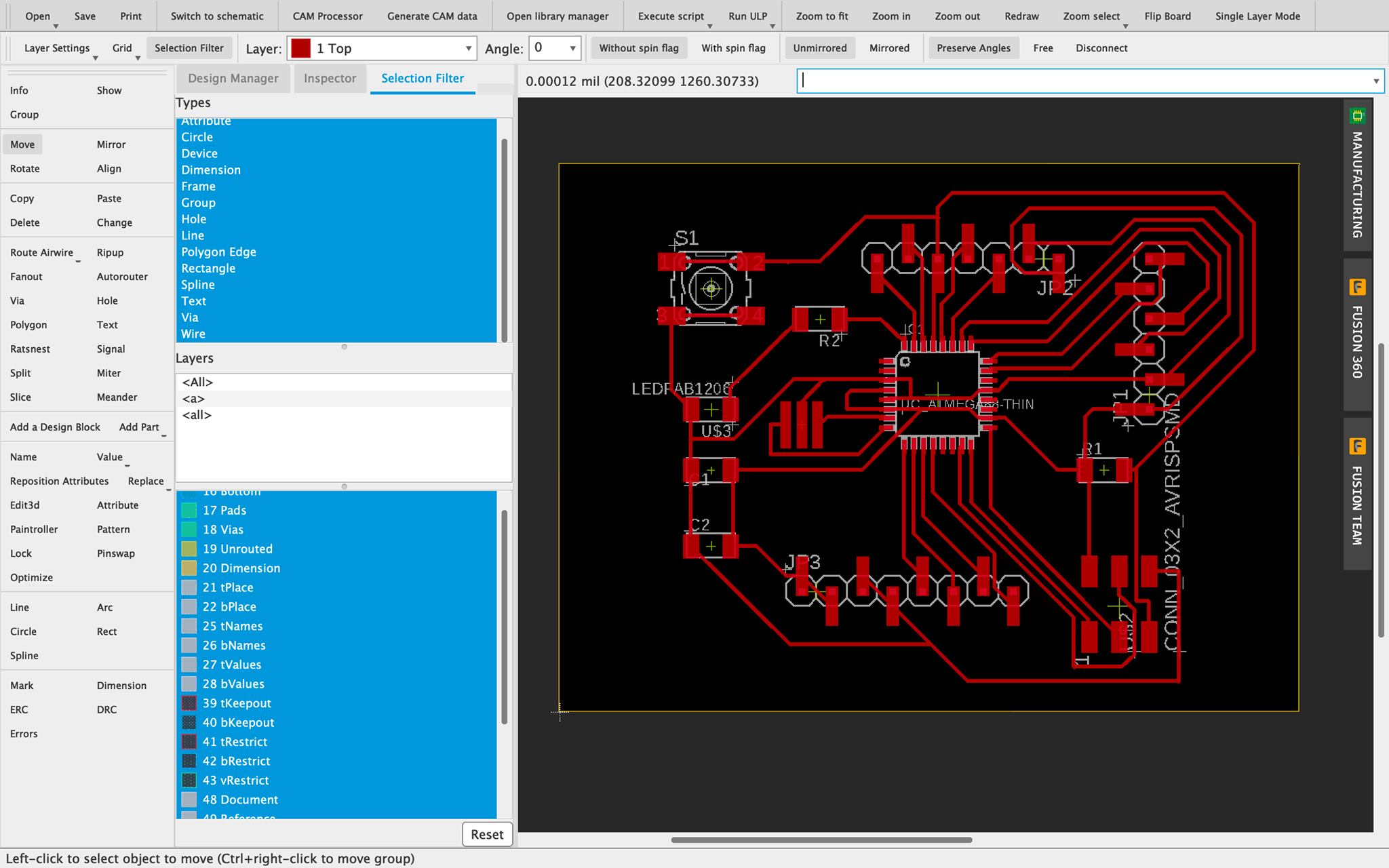
This is how the schematic file looks so far:
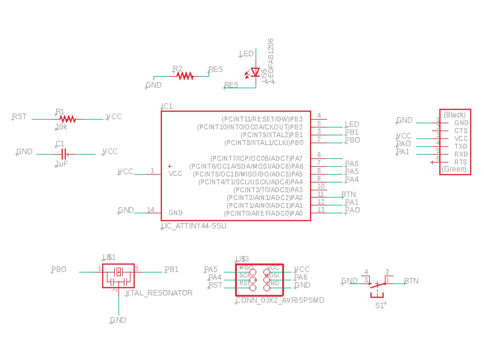
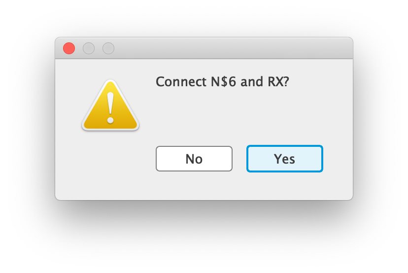
It is apparent in the sketch that the components I mentioned were connected are just floating in their space with labels. The trick is, those labels, when named the same, create wireless connections. I do this because it helps me avoid the confusion. When prompted to connect, as shown below, pick yes.
Layout/Board view
After that, I switched to the board view by simply clicking the Generate/Switch to Board button.
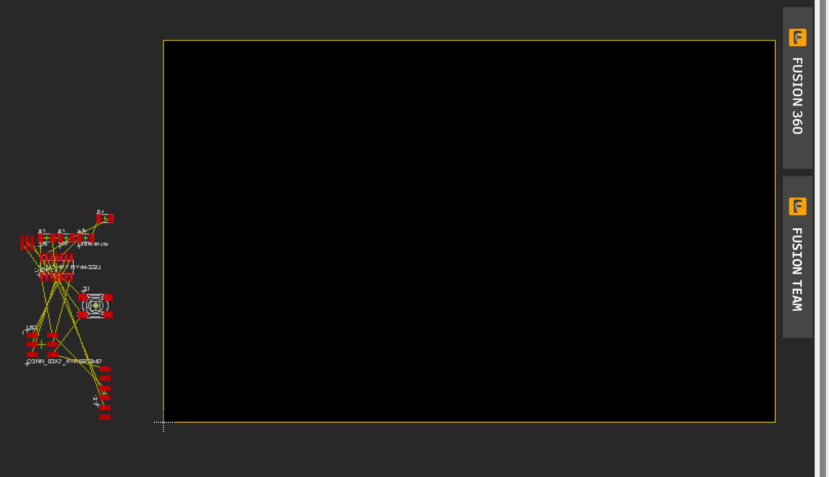
I moved all the components into the board using the move tool. Using the Route airwires tool, I connected the components following the thin yellow lines that indicate my connections in the schematic sketch…
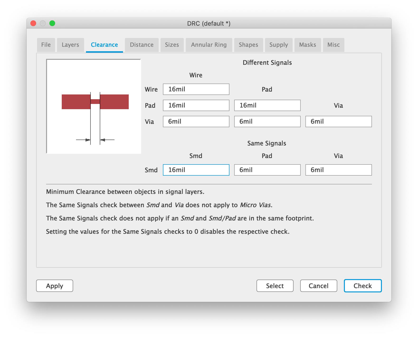
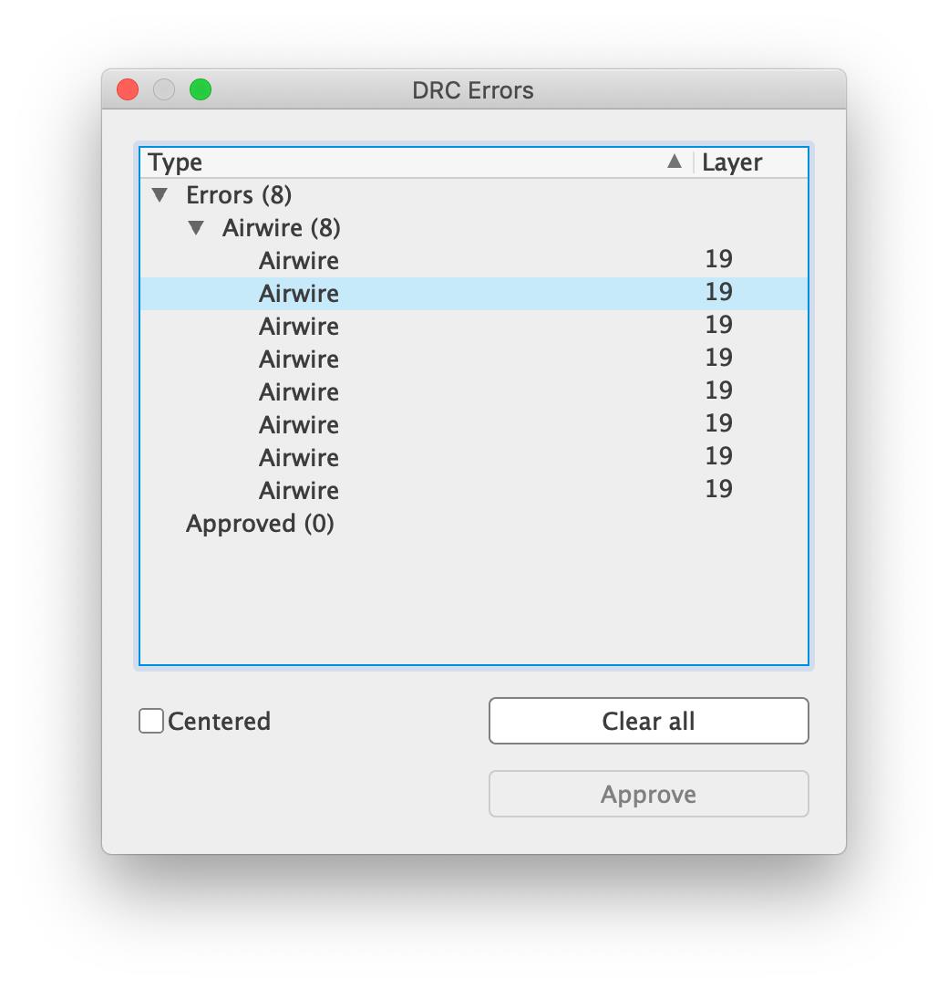
…then I performed the DRC (also known as the Design Rule Check).
At first, I set the clearance to 16 mil to fit our (1/64) mill bits at the lab, after I pressed check I got errors, many errors.
I searched this up and found this error is indicating some components were not connected properly, and to fix it, I navigated to the options tab in the layout editor > Set > Misc and then set the catch factor to 0. Then I edited the routes (Edit > Route) and moved my cursor to empty areas in the board and the nearest airwire would reroute and properly connect to clear the errors on the DRC.
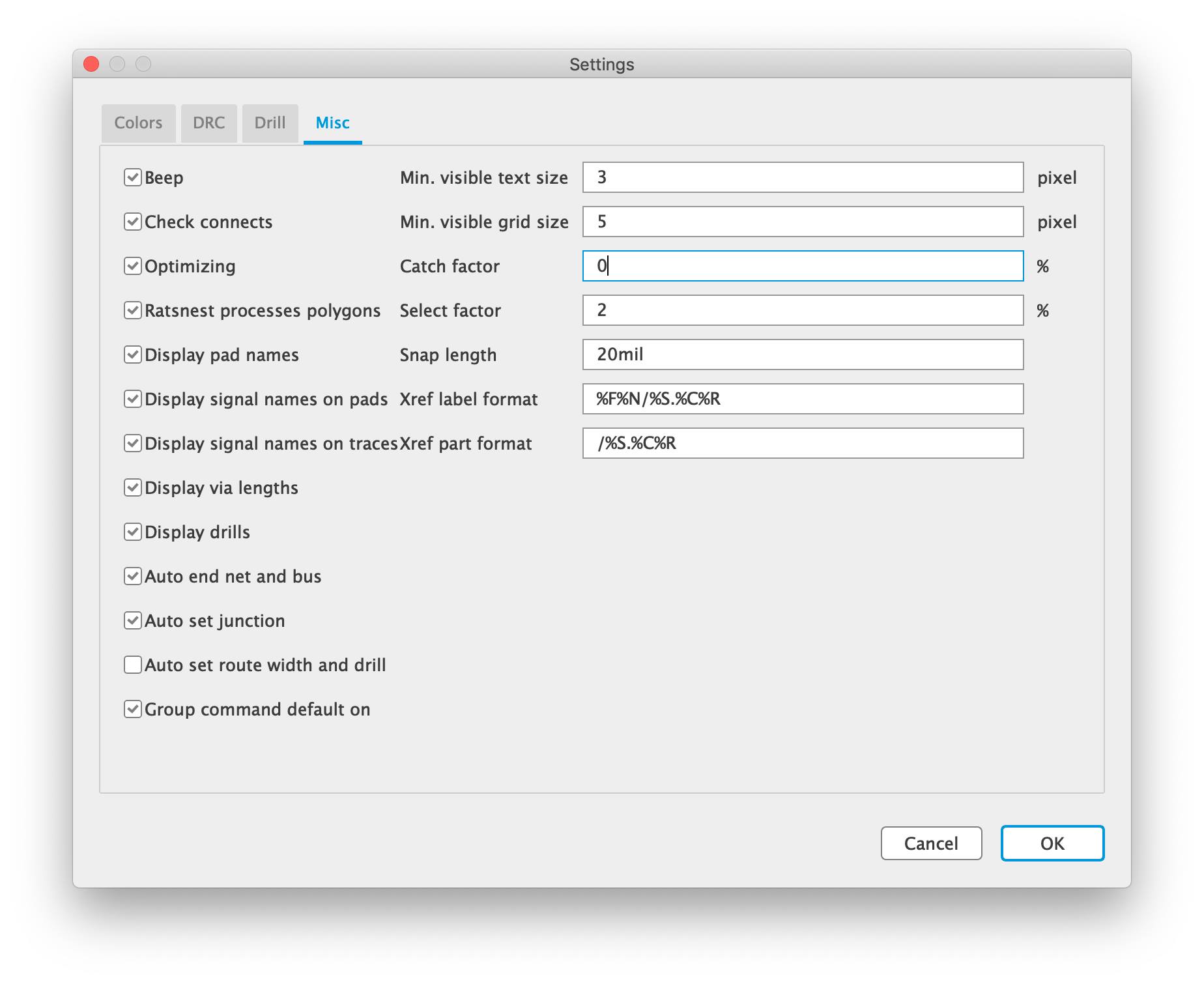
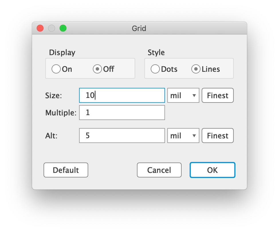
To make things move and relocate smoother, I also changed the grid to a size of 10 rather than 50 by going to the view tab > grid > and then switched the number out.
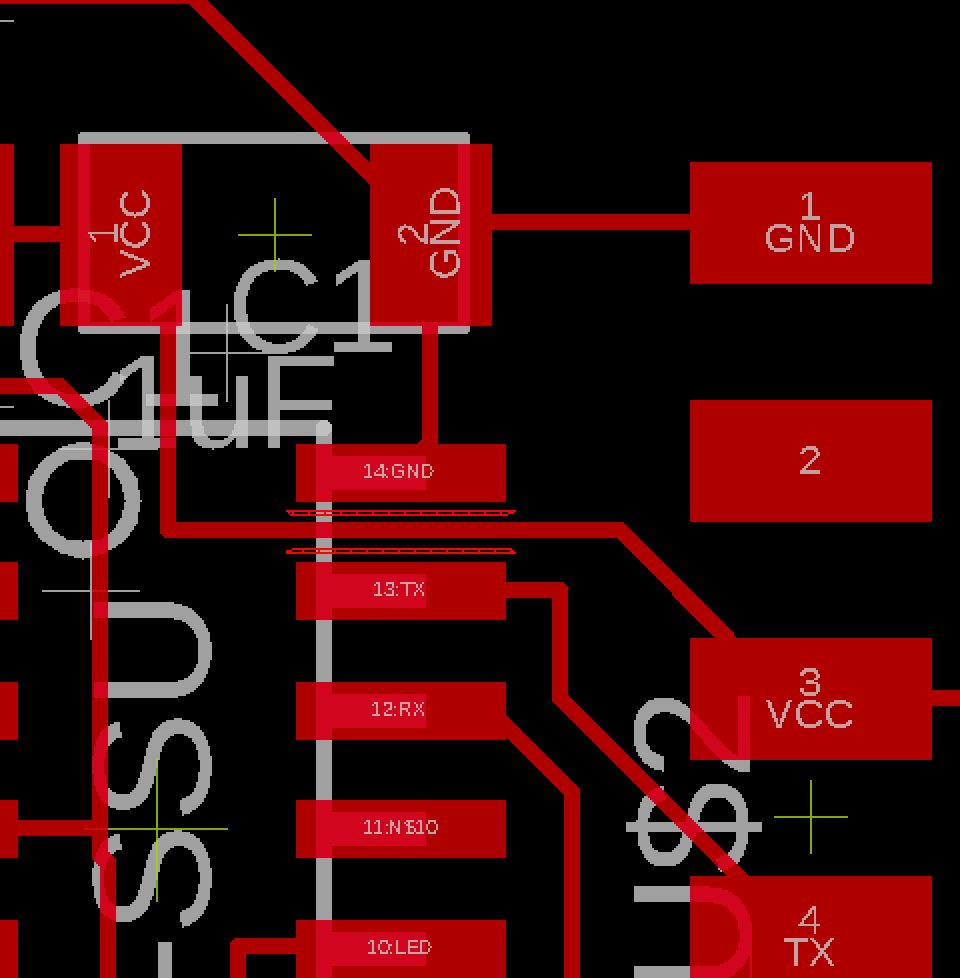
At last, I had 0 errors, but I could never be sure, so I ran another test, and yay! I got wire stub errors. Clearing this was simple, all I had to do was delete those little pieces of routing, and they were resolved.
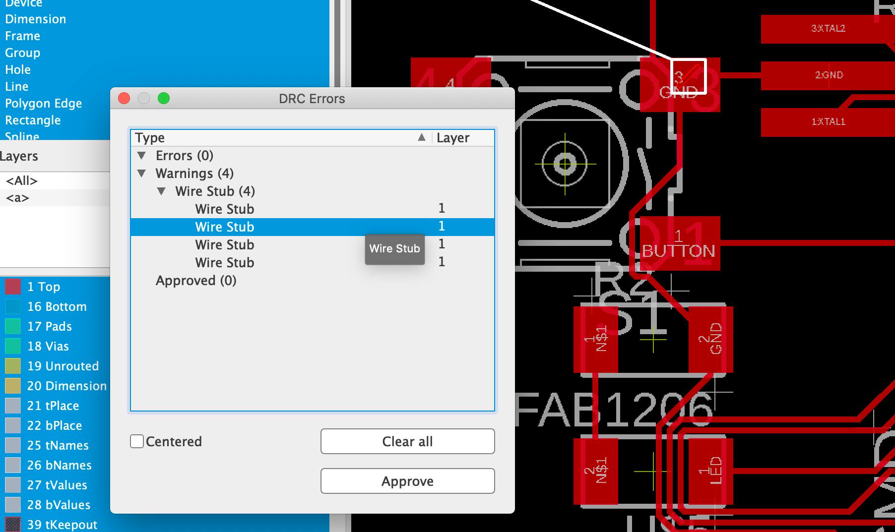
Just when I thought I was done, I had a clearance issue! The DRC done earlier for clearance was not applied using the apply button, rather it was just a check, so with more progress in routing, it was not checking whether they would match my DRC. Seeing how important clearance is, I redesigned my routes and started over from scratch.
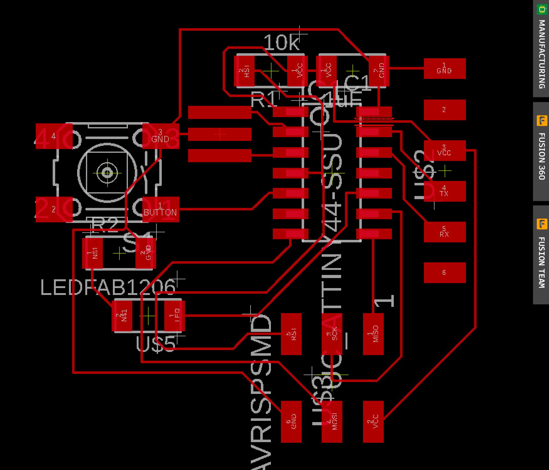
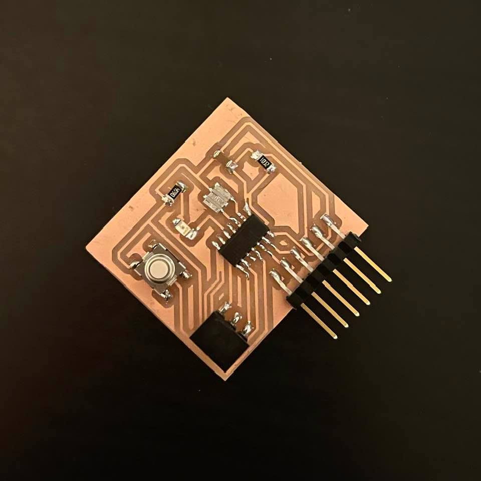
Finally, I was done. With zero errors, this is how my final board looked like.
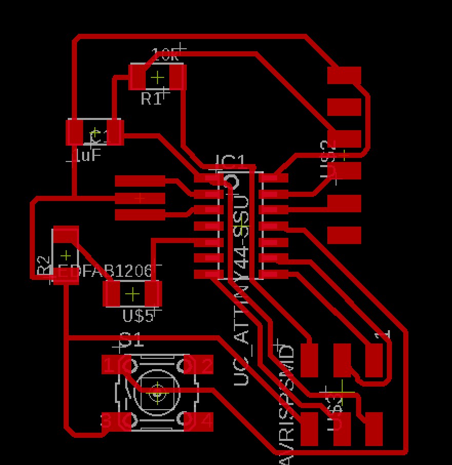
Don’t forget to resize your board to a smaller size that can accomodate the components and not take much of your board material (in my case, FR1).
Exporting the designs
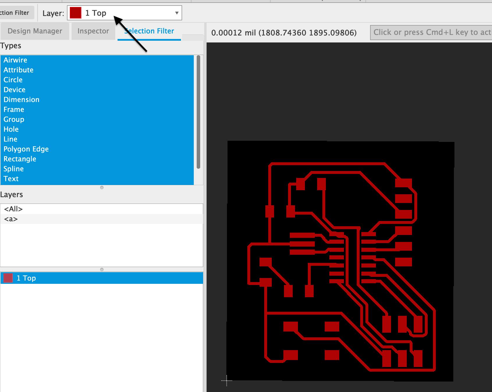
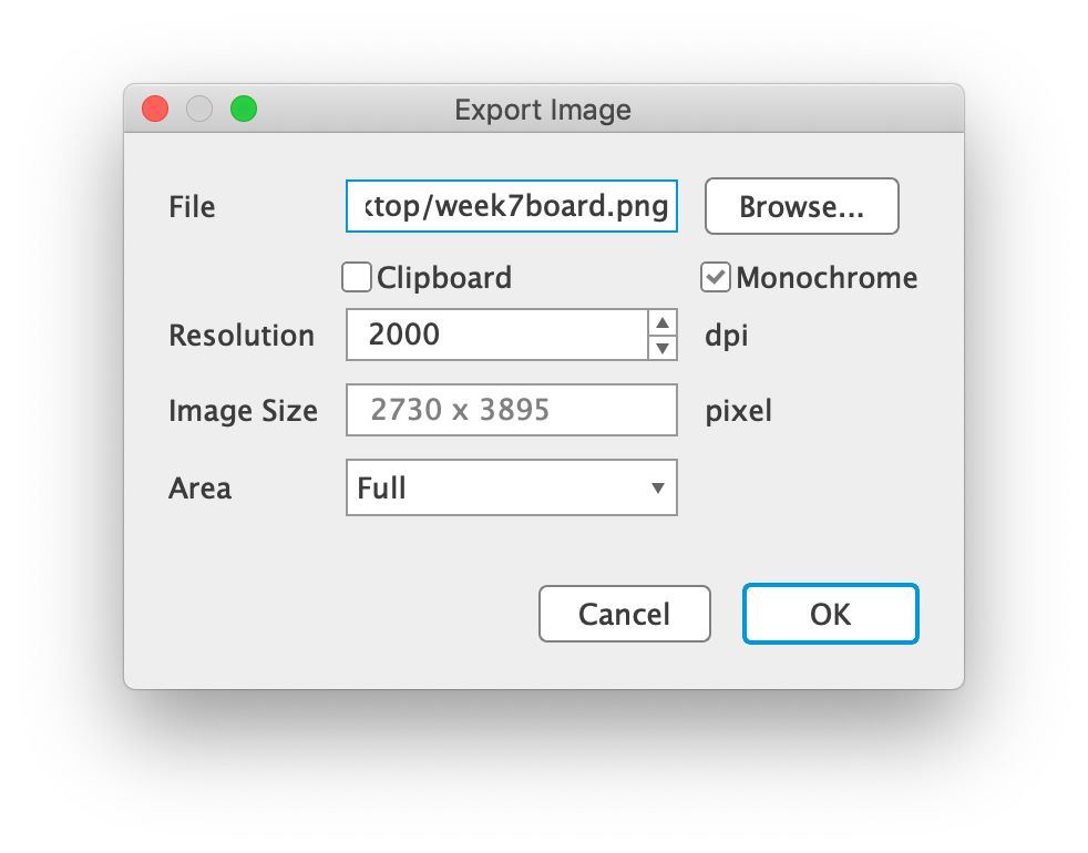
Now that the design is done, all that is left is to export it to be able to send it for miling. To do so, I started with exporting the traces. Since we only need the traces, I hid all the layers from view > layer settings, and then only showed the top layer. Then file > export > image > PNG.
Before saving, make sure to set your traces to monochrome, increase the resolution’s dpi - I set mine to 2000 - and you will need to jot down the image size since it will play an important role in scaling. Miling with wrong scaling will cause alot of problems.
Repeat the same process for the outline of the board; however in this case, hide all the layers from the layer settings and then export the image. Yes, you will be saving just a black block.
An alternative which worked better for my outline, was to duplicate the png of the traces, and using Preview, I added a white rectangle that covered the components. This white rectangle sets the dimensions of your outline, so make sure it is enough to accomodate all the traces.

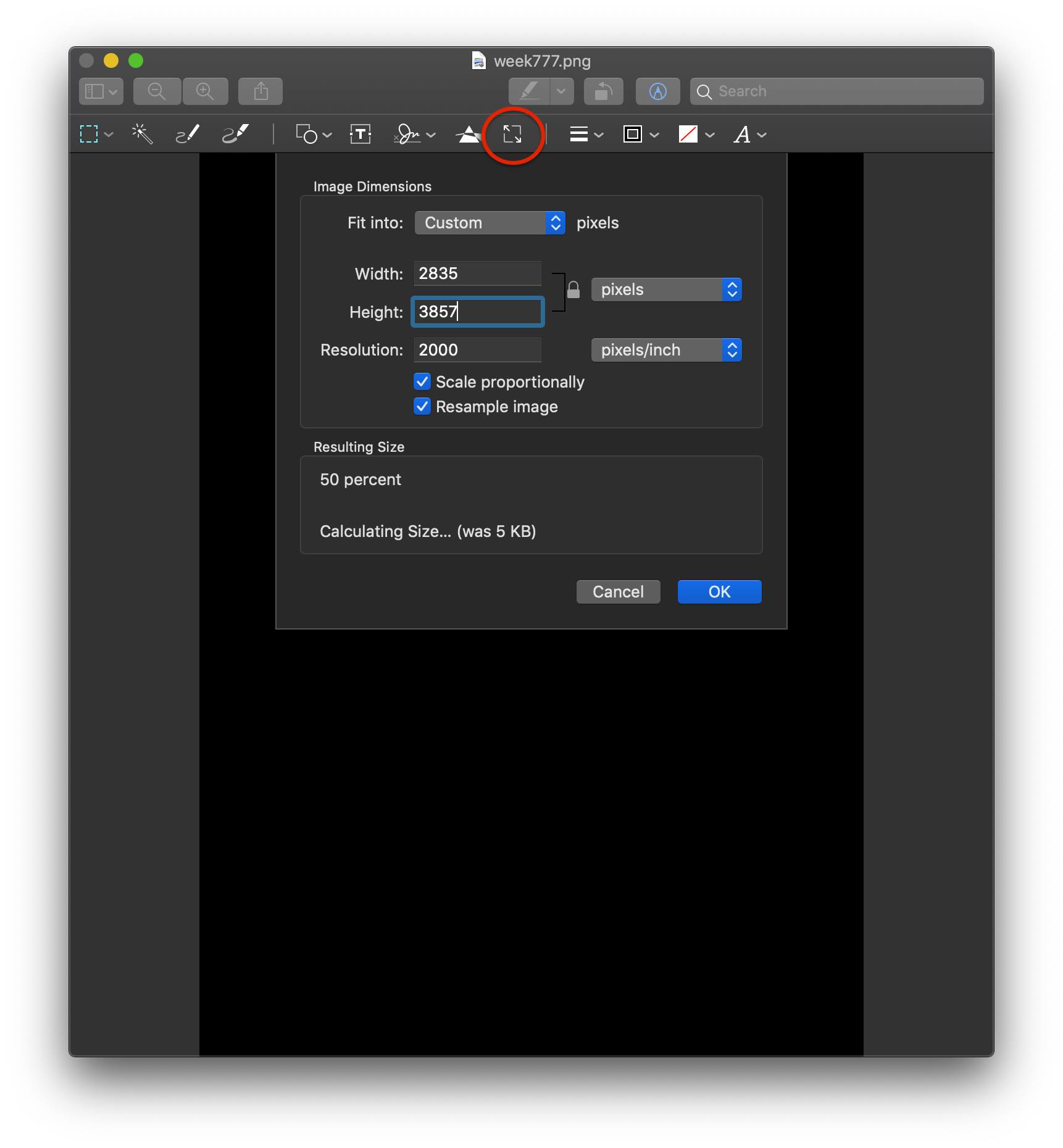
Now that you have your pngs, open them with preview and check whether the resolution and size of the image was tampered with. For me, my resolution was unchanged, yet my image size was. So, I just changed that to fit the size from Eagle, and then saved.
In the red circle is the tool used to make such changes on preview.
Then following the steps from the Electronics Production week, I deposited my pngs onto Fabmodules to get the .rml files, and saved them onto a flash drive.
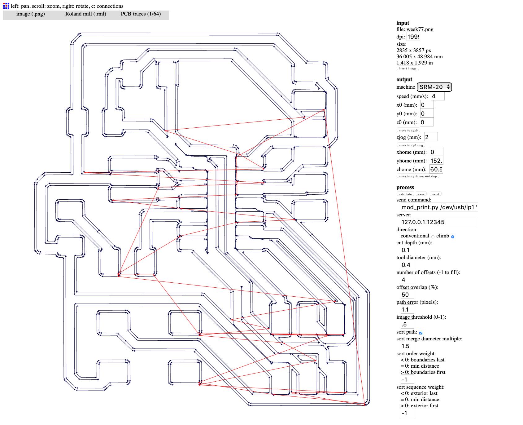
Producing the PCB
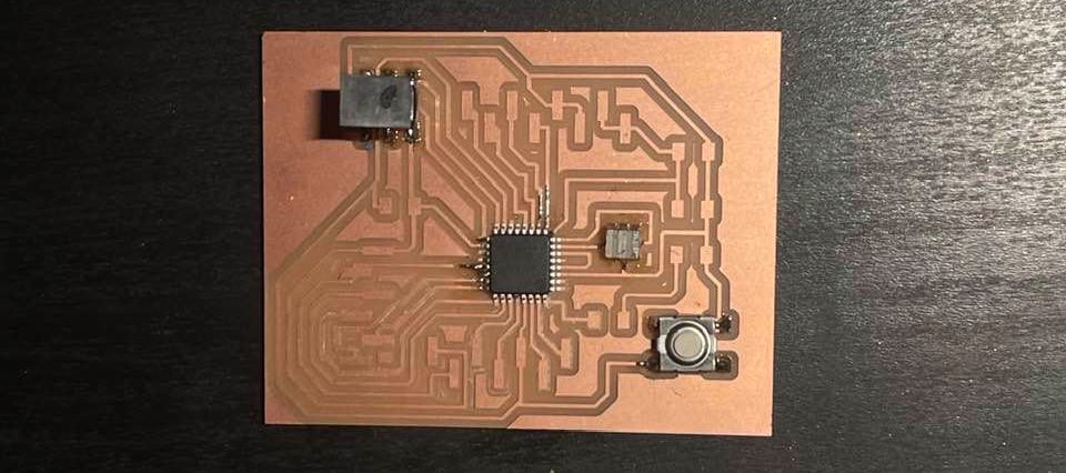
The following steps are exactly like the ones done in week 4, I set the X/Y/Z to an origin point by moving it to a space clear enough to fit the PCB. I used the (1/64) drill bit for the traces, and (1/32) for the outline. After milling was done, I soldered the components onto the board, and checked for short circuits using a multimeter, and voila!
I will program and test it in the coming week of Embedded Programming.
Fixing the error: missing connection
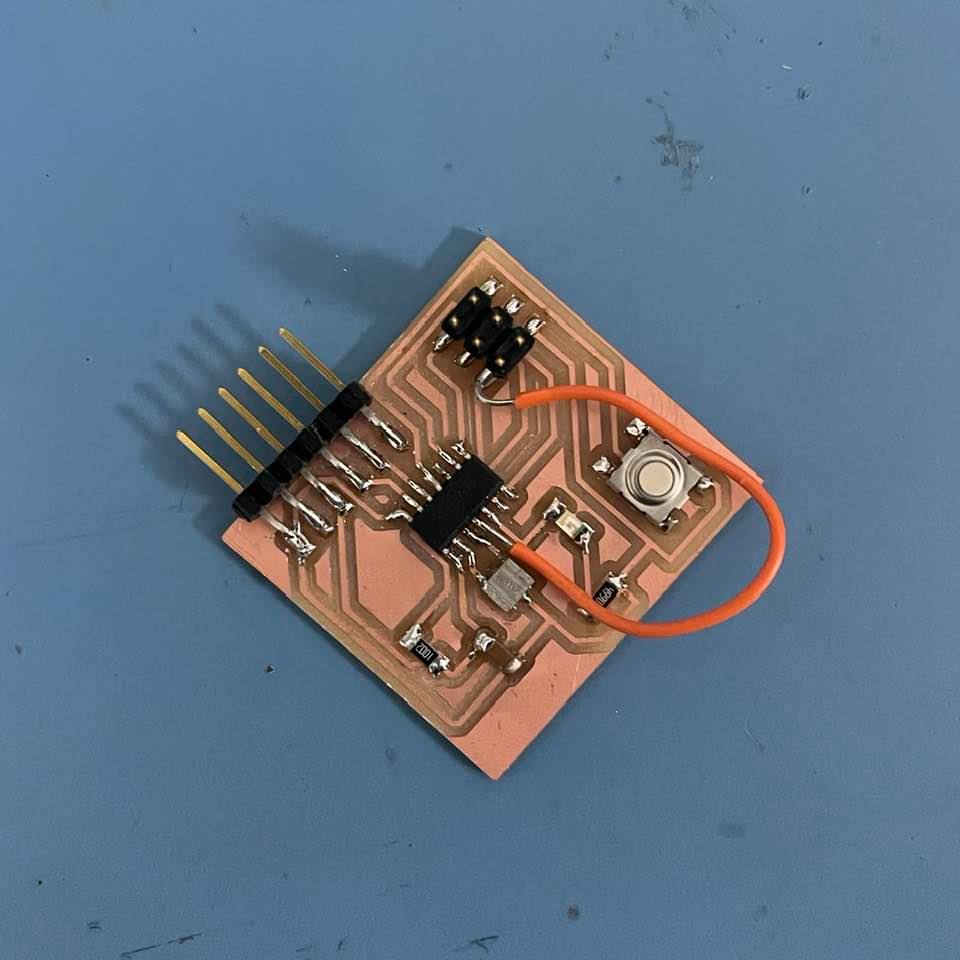
As mentioned at the top of the page, I had repeatedly missed a connection in my schematics of the ATtiny44. I milled and soldered around 4-5 boards all with the same error, until finally I realized that the error. I fixed it using a jumper wire connecting the RST pin of the ATtiny44 to the RST pin on the AVRISP.
ATMEGA328p-AU
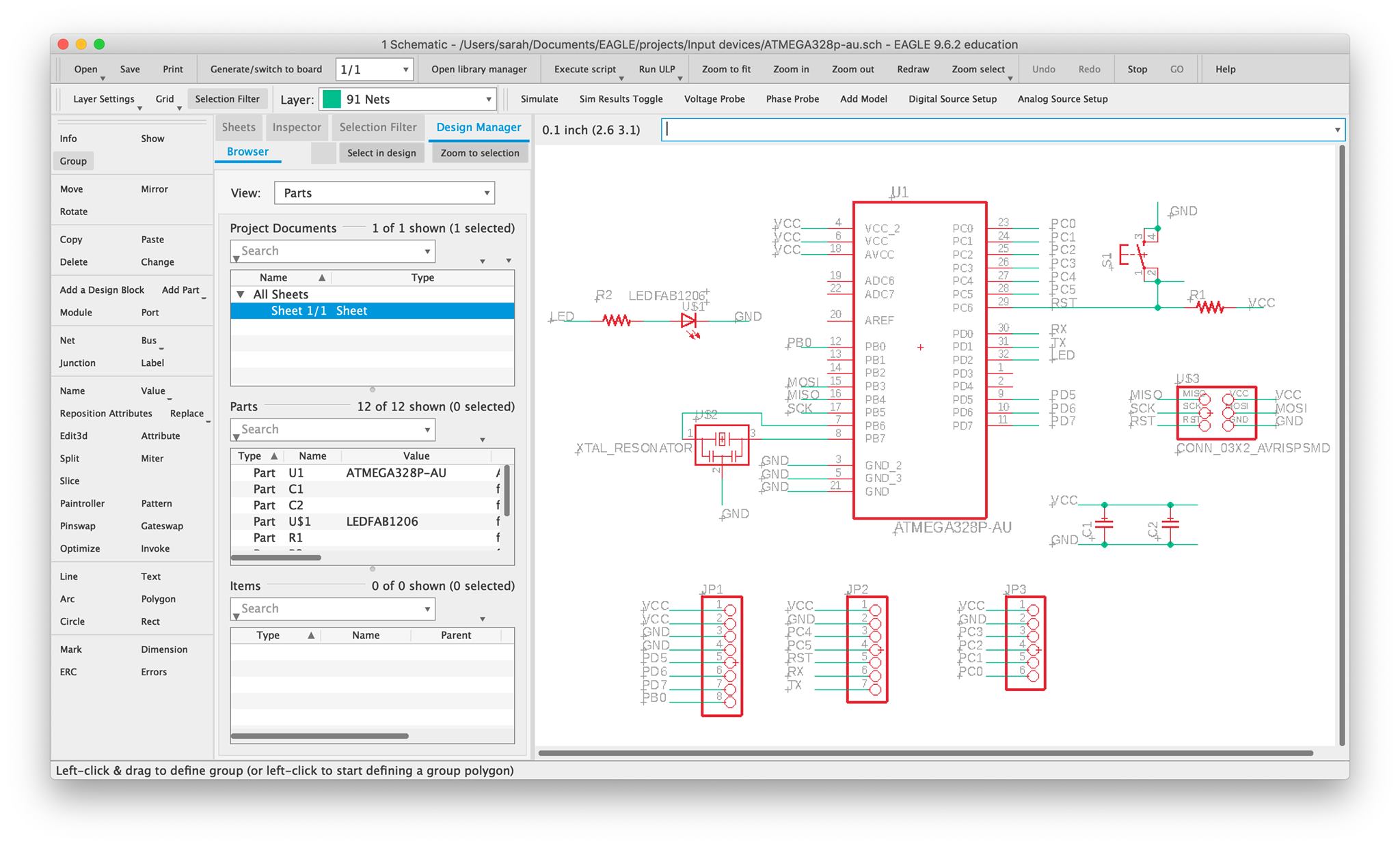
I knew I wanted my board to have many free pins, and an LED, and since electronics design isn’t my strong suit, I surfed the web for schematics I could follow. After much search, I found Lucas Lim’s board from his final project documentation. It had just the right amount of free pins, and fit everything I wanted my board to have. So, I started my schematic.
Designing
The list of the components I used are as follows:
| Component | Quantity |
|---|---|
| ATMega328P-AU | 1 |
| 10k Resistor | 1 |
| 1k Resistor | 1 |
| Unpolarized Cap 10uF | 1 |
| Unpolarized Cap 0.1uF | 1 |
| LEDFAB1206 | 1 |
| ISP Header 2x3 | 1 |
| Button switch | 1 |
| 20Mhz Resonator | 1 |
| Connector Header (1x6) | 1 |
| Connector Header (1x7) | 1 |
| Connector Header (1x8) | 1 |
The completed schematic sketch is as follows:
Milling + Soldering
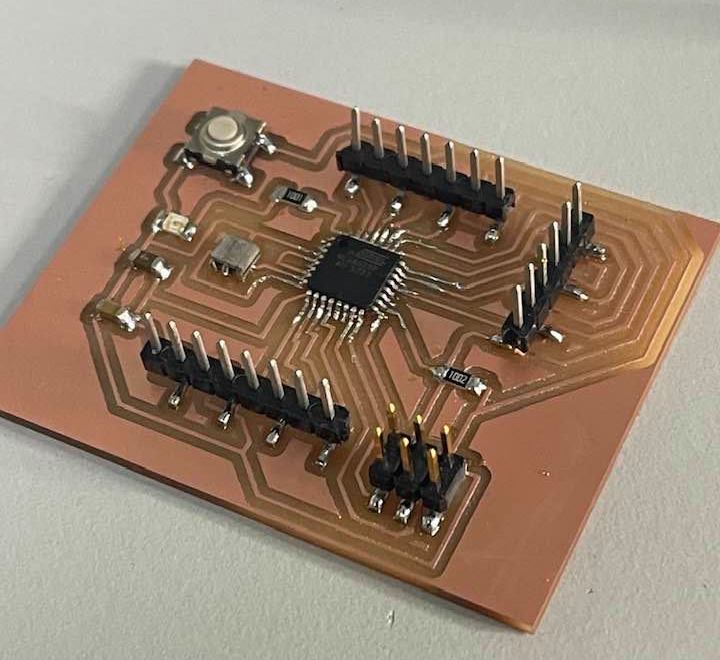
I have yet to complete soldering, but as you can see a short circuit exists between the pins of the ATMEGA. This is because I tried soldering it using my solder gun at home, which doesn’t work very well. I’ll have to redo it soon.
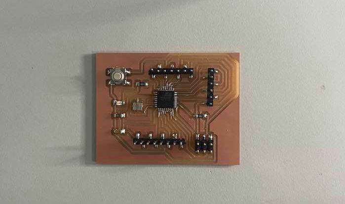
Update May 1, 2021: I redid the milling and soldering, and final board looks as follows:
Programming
To be done on-demand (You can see it being programmed in Week 14: Networking and Communications).