Step-by-step: from project to PCB
1) Create a new project
First, I created a new project to keep all files together (schematic, PCB layout, and fabrication outputs).
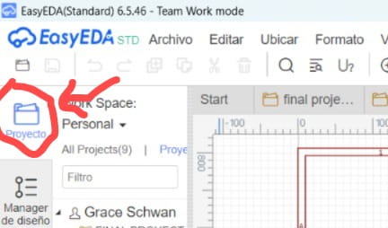 Figure 1. Starting point in EasyEDA: create/open a project from the left panel (Project icon).
2) Place components (from the library) and build the schematic
In the schematic editor, I added the main parts of my board by selecting components from the library panel (left side).
I searched and placed symbols such as connectors/headers, the XIAO RP2040 module symbol (or equivalent pin headers),
and the module connections for my project (TCS3200 and DFPlayer Mini).
After placing the components, I wired the signals using the routing tools and organized the circuit with clear net labels
(e.g., VCC, GND, TX/RX, and sensor control pins). This schematic became the reference to generate the PCB connections.
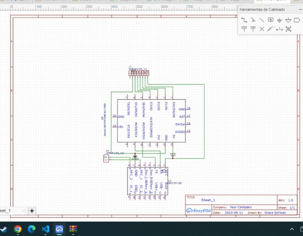 Figure 2. Schematic created in EasyEDA: XIAO RP2040 + connectors/modules wiring for my final project board.
3) Convert to PCB and place footprints
Once the schematic was ready, I switched to the PCB editor. EasyEDA brings the net connections (ratsnest) so I could place the footprints
and keep related parts close together. I arranged the connectors to make the board easier to wire and test.
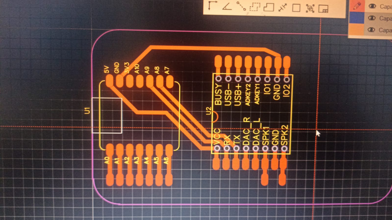 Figure 3. PCB editor: footprint placement and the first routing steps.
4) Route the tracks (copper traces)
After placing components, I routed the copper traces. I followed the ratsnest connections and kept enough spacing between tracks and pads.
I also added silkscreen labels (text) to identify the board and connectors.
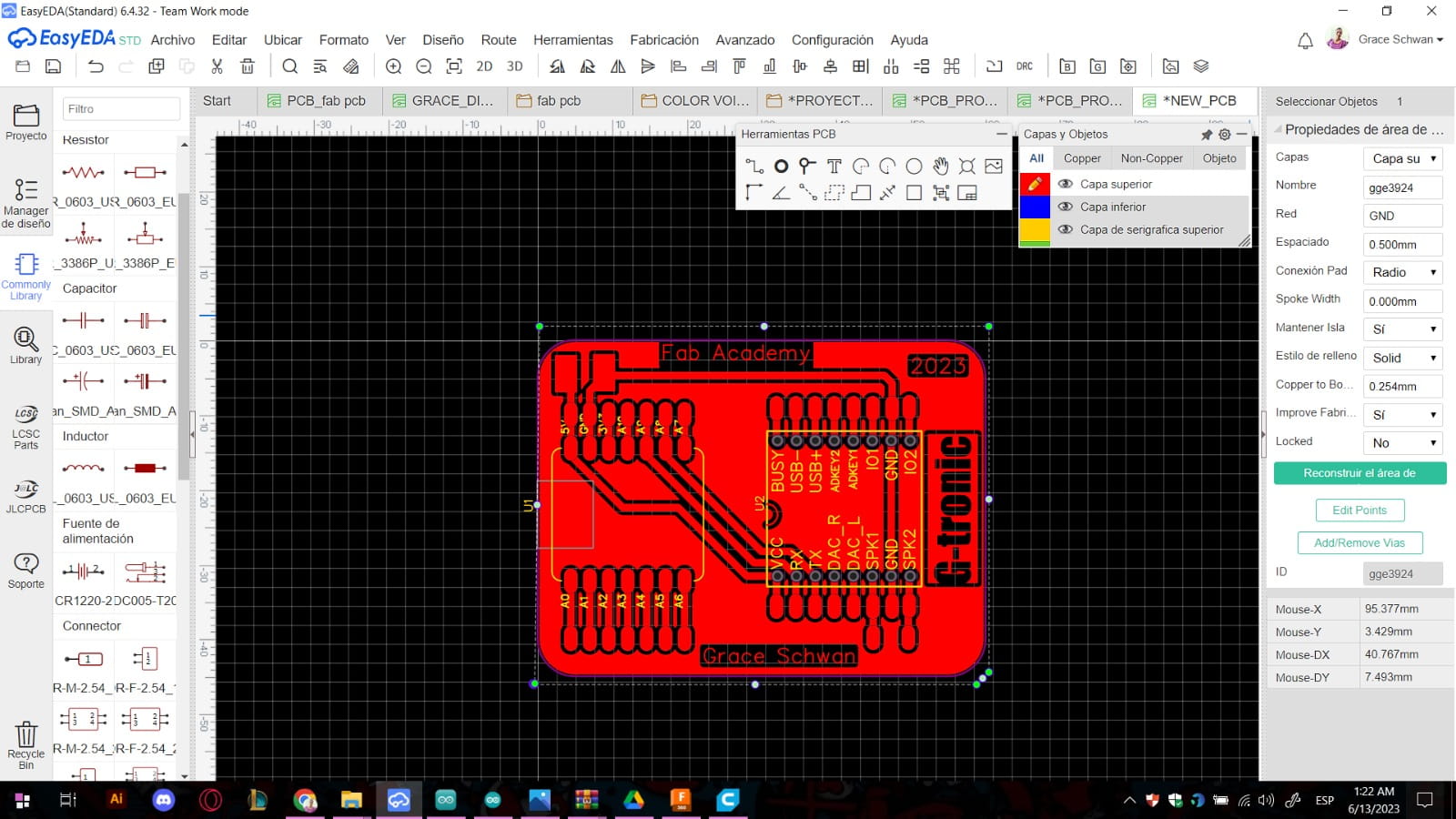 Figure 4. Routed copper traces (tracks) on the PCB.
5) Define the board outline (shape)
Next, I defined the board outline (the final shape that will be cut during fabrication). I used a rounded rectangle to keep the board compact
and safe to handle.
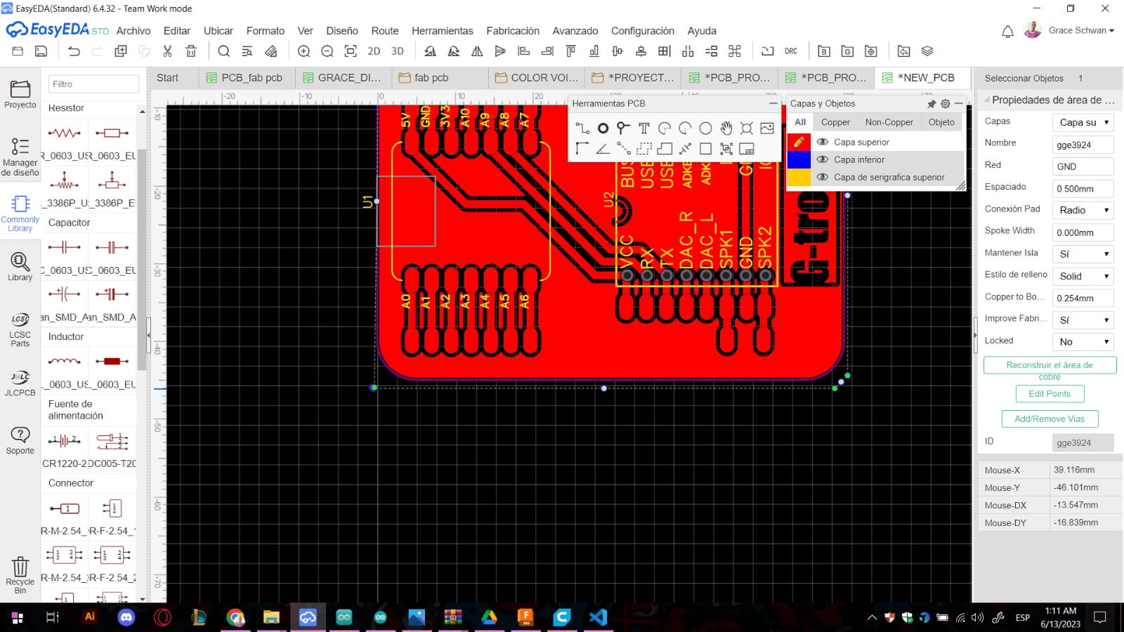 Figure 5. Board outline defined in the PCB editor (final cut shape).
6) Generate Gerbers and review fabrication information
When the routing and outline were finished, I generated the Gerber fabrication files directly from EasyEDA. The tool also provides
a preview including the number of layers, dimensions, and an estimated manufacturing cost, which is useful for planning fabrication.
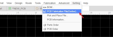 Figure 6. Gerber generation and manufacturing preview (layers, dimensions, and cost estimate).
7) Final step: 3D visualization
Finally, I used the 3D View to visually inspect the board before fabrication. This helped me confirm component placement, pad alignment,
spacing, and the overall appearance of the PCB.
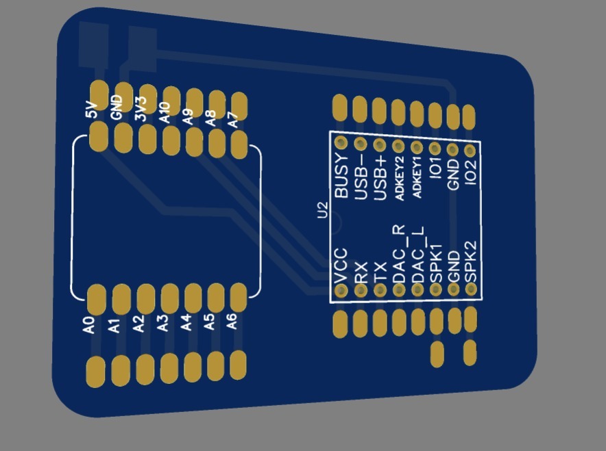 Figure 7. EasyEDA 3D visualization of my PCB (final inspection).
8) Cost estimate inside EasyEDA (manufacturing preview)
One feature I found really useful (and honestly amazing) is that EasyEDA can also show a manufacturing preview with an
estimated PCB cost. After generating the Gerbers, the platform displays key information such as the number of layers,
board dimensions, quantity, PCB color options, and an approximate price. This helped me understand the real size of my design
and quickly evaluate fabrication options before producing the board.
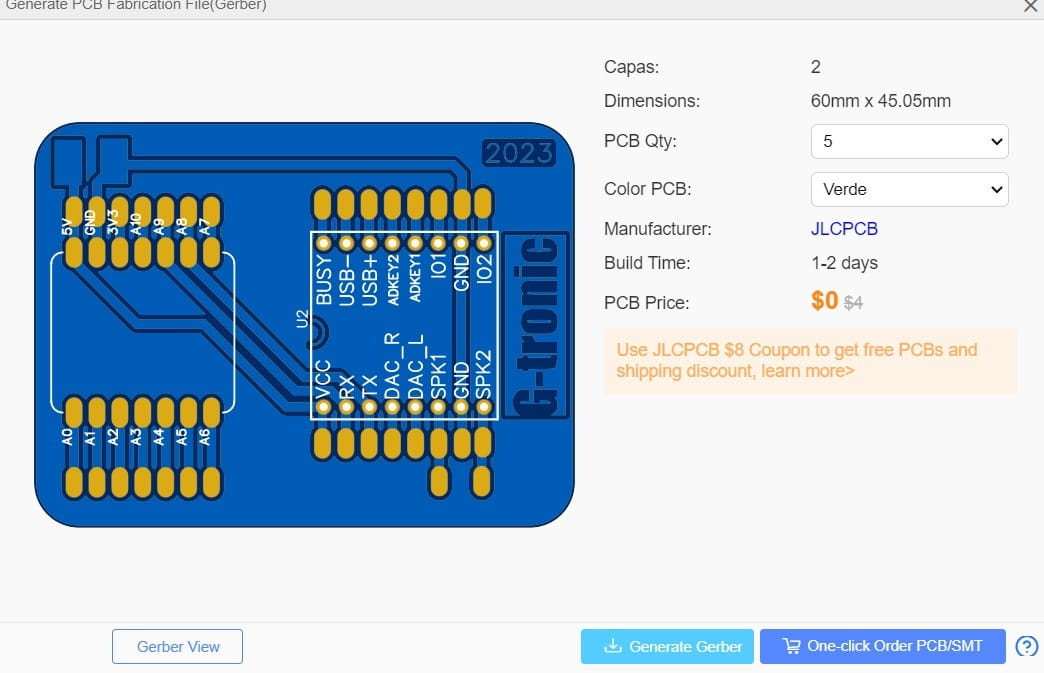 Figure 8. EasyEDA Gerber generation and manufacturing preview showing layers, dimensions, quantity, and the estimated PCB cost.