7. Electronics design
This week is dedicated to learn the tools to be able to design electronic boards. As an architect, I have always wondered how these were conceived: I find the layout of many of them trully fascinating, and I even sometimes I have used them as inspiration when starting a project for a competition. But I have absolutely no idea of the how are they designed, nor why do they end looking the way they do. Let's see what can I learn during just this week.
Replicating the "hello ftdi 45"
First thing I did was not to follow our local instructors advice and install kicad instead of Eagle. I know that I will regret it and end up doing what they recommended, but, for now, I just used sudo add-apt-repository --yes ppa:kicad/kicad-5.1-releases and sudo apt install --install-recomends kicad.
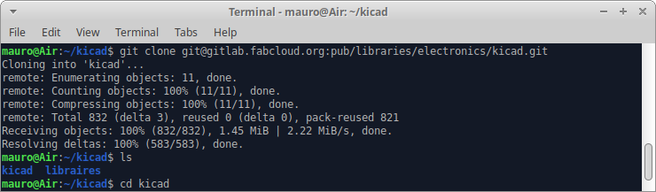
Next step was to install Fab Electronics Libray for KiCad. I cloned the repo, since I think it will be easier to update if neccesary. Since I am completely starting in electronics, I thought that would be a good idea to start from scratch, and only use the Fab Library, so when given the option, I created an empty global symbol library table
Then I set both symbol and footprint libraries and added the variable FAB in the "Preferences/Configure Paths" dialog.
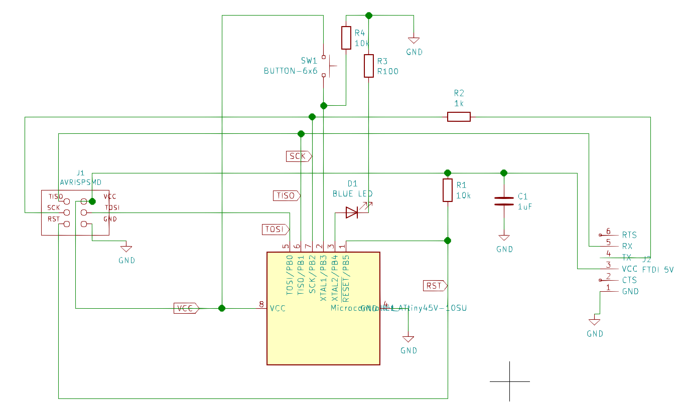
Once done configuring, I started my first project, the hello.ftdi.45. I started trying to figure out how the schematics is, just by looking at the footprint picture, while at the same time working my way around Eeschema. I find the zoom a bit clumsy, and the wire thickness too thin. I only managed to change the latter, in the General options menu.
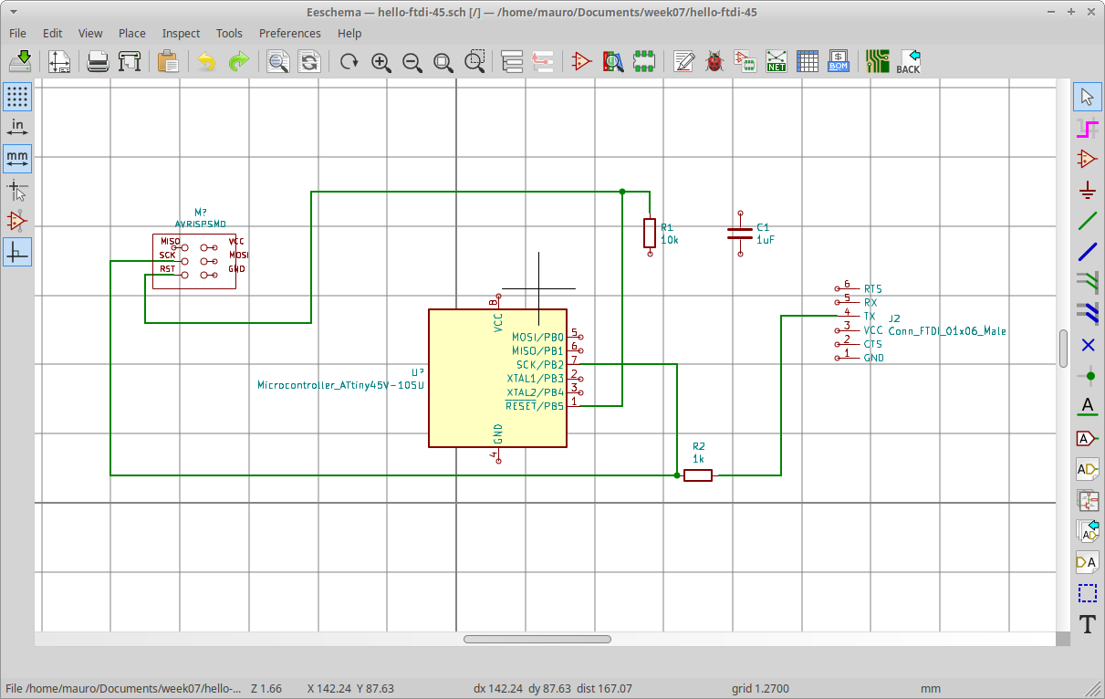
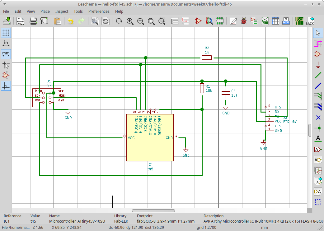
I populated with the scheme with a few symbols, which I scattered over the canvas more or less in the same place they are in reality. Then, started to wire them. But I saw that there were going to be a lot of wire intersections, so I tried a different strategy. This time I got it with 3 crosses, which I don't know if it is readable enough or not. To me is total foreing language...
After a break, I went on with the Pcbnew module. First difficulty was that I was not able to set a single sided board. I searched in the Kicad forum, and almost everybody agreed that the way to achieve one side was either not using the auto route or set it not tu use the F.Cu layer.
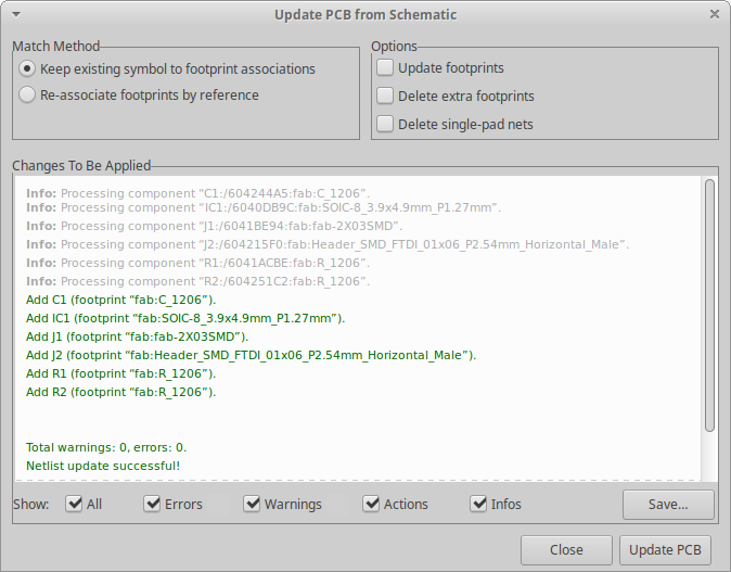
The next problem was came when I tried to update the board from schematic:
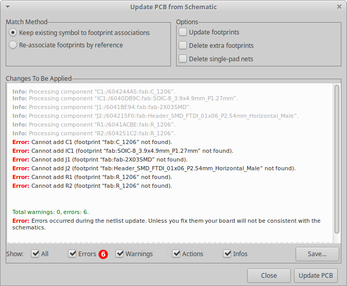
I reviewed all the setup instructions steps, to try to find my mistake, but could not find any. Then, in Eeschema, I found that every component has a place where it states where the footprint is. Clicking on the icon with a few books, promted this message:
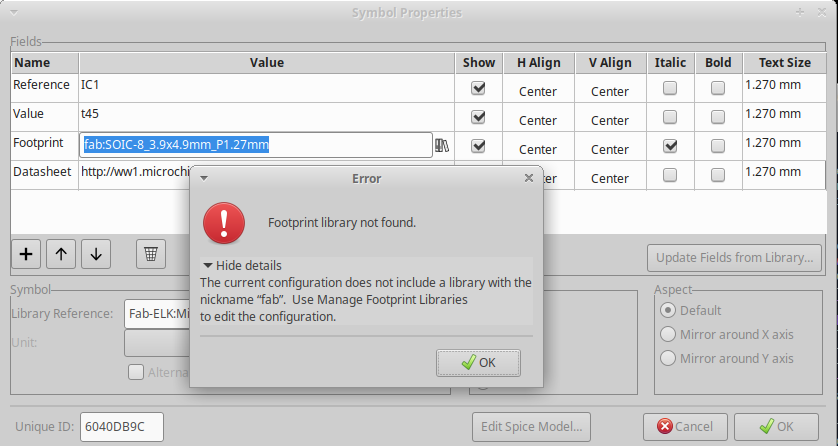
So that was it: the nickname of the library should be fab and not Fab, as I had used. I went on to change it and now it worked fine!
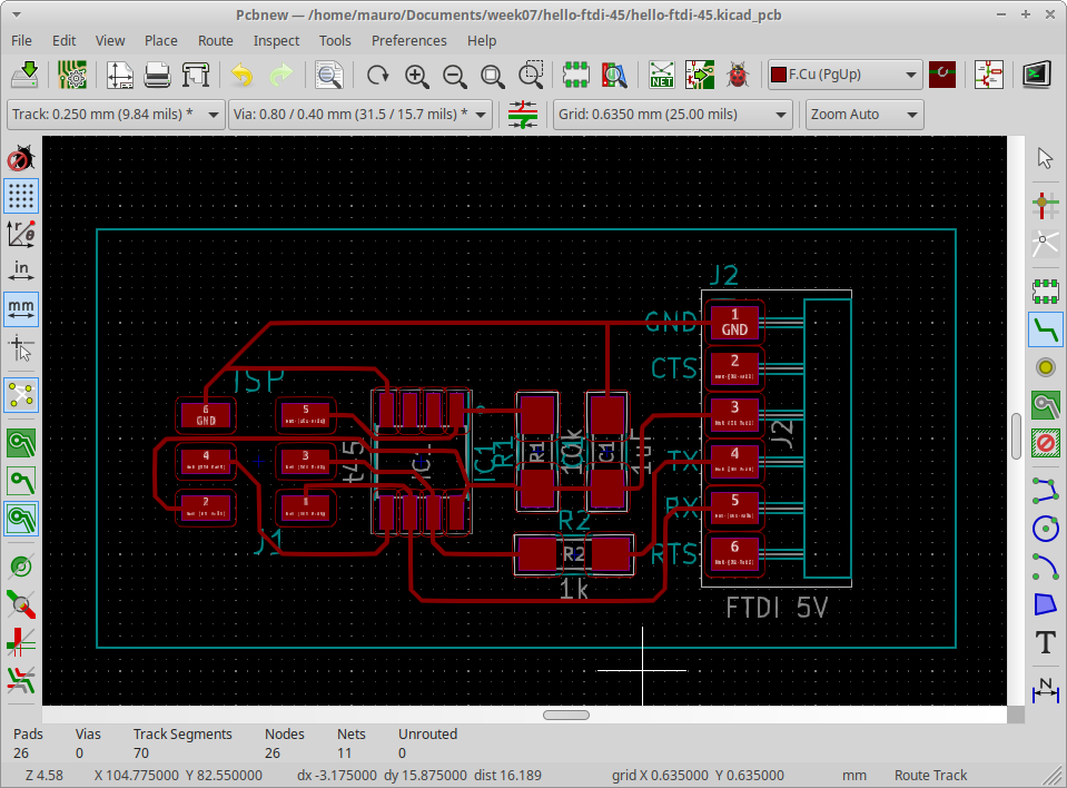
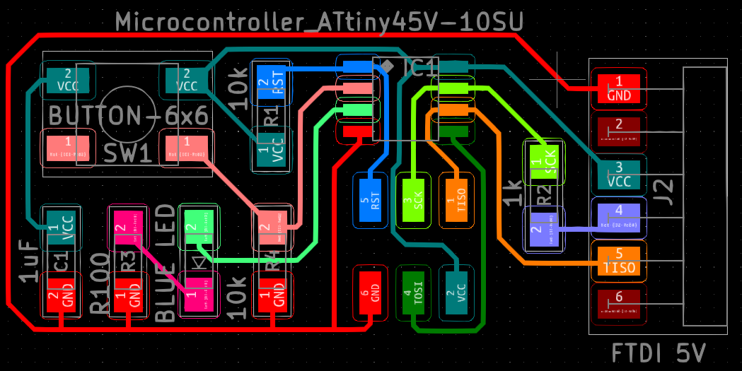
At this point I can't really tell, but it seems to me that the traces for the microprocessor are smaller than the ones in Neils footprint. I will print it before milling, just to check it. I did not add any autoroute plugin, so I did the routing by hand. After finishing the first time, I noticed that I did not check the track width or the maximum clearance. Then, I set both to 0.4 mm. I know that the track could be smaller, but let's try with the same as the minimum distance between lines. With this setup, I could not fit the four traces that Neil has fitted underneath the AT Tiny 45, so I reduced the track width to 0.25 mm, and finally ended up with:
Later, I'll have to figure out how to export it to png or svg, so I can get the g-code to mill it in mods.
I wanted to keep this hello board, save as hello-modified, and edit that one, at least it was the workflow that I expected... but there is no "Save as" in Kicad. The closest I found was to create a user template, so I followed the instructions to have a template for the AT Tiny 45 hello board, including the info.html file with a brief description of it.
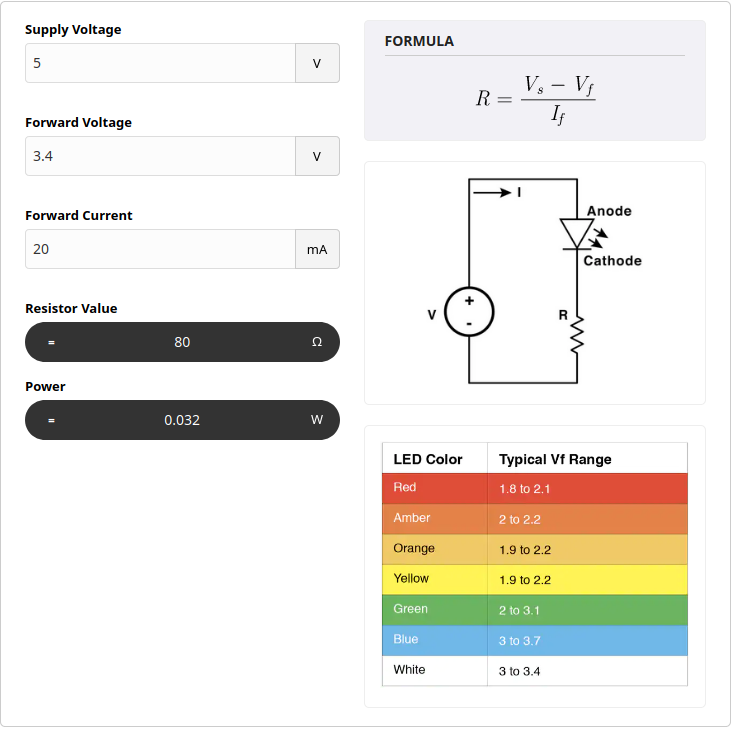
For this week's assignment I need to add at least a LED an a buttom. Yes, I know... the at least is kind of inviting to do more... but I am going to keep it simple for now. I am indeed still a noob in electronics. I do not even know where to add those two new elements. My guess is that there are two free pins out of the AT Tiny 45, so I will use those two. I have learned earlier this week that an LED needs limiting current resistor, otherwise the amperage will ramp up to the maximum the power supply can handle and will burn the diode (I=V/R, no resistor, R is close enough to 0 to make I as huge as it can phisically get). To calculate the size of teh resistor needed, I used the LED data from the vendor:
- Forward Current: 20 mA
- Forward Voltage Red: 1.8 V
- Forward Voltage Yellow: 2.1 V
- Forward Voltage Green: 3.0 V
- Forward Voltage Blue: 3.4 V
- Forward Voltage White: 3.0 V
The led is going to be blue, using the formula R=(Vs - Vf)/ If, an 80 ohm resistor is needed. Digikeyis kind enough offer a calculator, and advices to use a device with power rating 2 to 10 times higher than the 0.032 W, to avoid excesive heating. The resistors in the inventory are 0.25 W, so we are in the safe side.
I tried to redesign the board, using 45 deg angles, and with the components around an octogon. Found very useful the keyboard shortcuts e, to access the properties of an element, and m to move an element, even nudge it with the keyboard. It was very useful also to find the icon "Highlight net": a net is just that, all connected pads with their tracks. My first attemps were very clumsy, so I decided to keep it simple for now, and went back to the comfort of orthogonality. I did not find a command to delete all tracks at once To delete all tracks at once (or other elements), under the edit menu, use "Global delete".
Getting all the components properly connected is way harder that I had anticipated, at least trying not using bridges. Using net highlighting is very useful when solving this geometric sudoku, so I tried to find a way of assigning a different color to each net. I could not find how to do it, and then I found an article by Peter Dalmaris, and this feature is present in the next release, already availible in the nighty build. So I followed instructions to install it and check it out.
It turned out a great move. The new version is, in my opinion, way more user friendly. Zooming in and out is much smoother, and, at least for a newbie like me, being able to assign colors to different nets, is a complete game changer. If the buttom works the way I expected, then I am really happy with the result, since I solved this sudoku without looking at the answer. I also labeled the nets in Eeschema, which help a lot clarifying everything, and changed MOSI & MISO for TOSI & TISO - Teacher - Student element relationships. I also added a poligon as a border line of this PCB, in the 'edge-cut' layer.
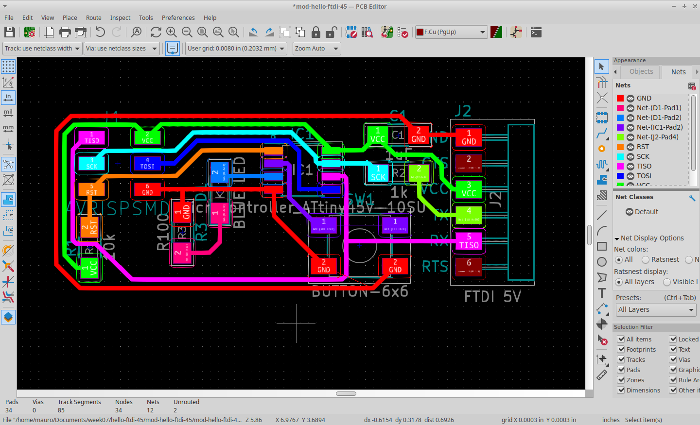
After a review with the instructors, I learned that I got wrong my schematic, since I did not connect the button to gnd, microcontroller and Vcc. And once againg, pull down and pull up resistors wer explained to me. I reviewed the schematic with Adrian (hey, thanks a lot), and went on again to the sudoku solving phase.
This time, my self imposed goal was to end up with a compact pcb, while not using 0 omh bridges, and again coloring nets was very helpful. It took me a little longer to solve it this time, maybe it was just because it was late, and I was a little tired. I really hoped this time worked, because it seems weeks gets shorter as the course advances...
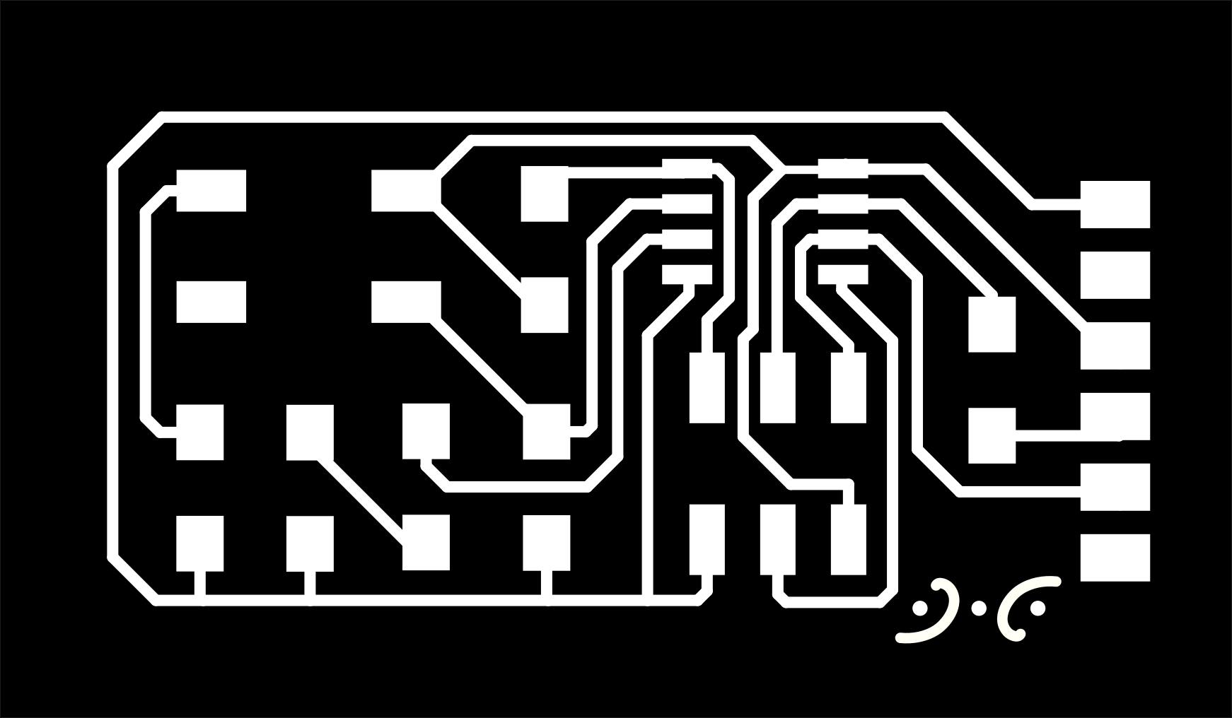
The next step in the workflow was using the plot command in Kicad. I exported both the F.Cu and the Edge-cut layers, choosing the option inverse output. The output format was svg. I tried to import it directly into mods, but could not get it directly. I will have to check later if it was due a units problem. I opened it in Inkscape, and converted them in png files, at 1000 dpi. For the edge cut, I also did a boolean between the outermost part and the inner line. Finally, in mods, I used the settings that worked with my machine two weeks ago:
- Feedrate: 6 mm/sec
- Plunge rate: 2.5 mm/sec
- Spindle: 16,000 rpm
- Pass depth: 0.1mm
Design files
Fabrication process
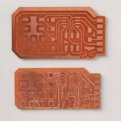
The first cut was going fine, but when finished, I realized that I drew the outline too close to the traces, and did not accout for the 0.8 mm of the cutting end mil, so some of the traces dissapeared in some points. I also noticed that the minimum 12 mils track width I had set as the desing rule was too optimistic, so I changed it to 16 mils. The 1/64 end mill broke while milling the first board, but since it still had a quite long cutting part, I tried to set zero again and keep using it. The result, mostly in the bottom of the board is not optimal, I guess it could improve by filing a little bit the end mill, but for the next PCB I decided to use a new end mill.
The workflow was quite easy: once a part of a track is selected in Kicad, pressing U selects all connected parts, and pressing E opens the track property dialog, with the width field preselected. I then drew the outline in Inkscape, this time allowing a much wider space between track and the edge of the PCB (probably too much this time), and also I reffited the logo that I used, just enough to meet the design rules. Milling went fine, so I milled a second board, just in case I mess up soldering components.
One part of this workflow in which I will have to spend more time is defining the board edge. I did it in Inkscape, and I will need to get more aquinted with the proper tools to work with paths, considering the requiered precission. I did like how straightforward it is to export as png. I set the resolution at 1000 dpi, following the examples that I had previously used in mods
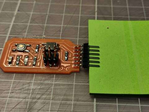
When I was going to solder the ftdi pin header, I noticed that I should have made the board a couple of milimiters longer on that side, so the plastic bit would have support. I used a small stack of post-it to build the step so the header would stay horizontal while soldering. It was a good trick, that made the task so much simpler. After I had struggled with the microprocessor, this pads and part just seemed gigantic.
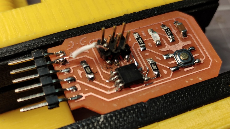
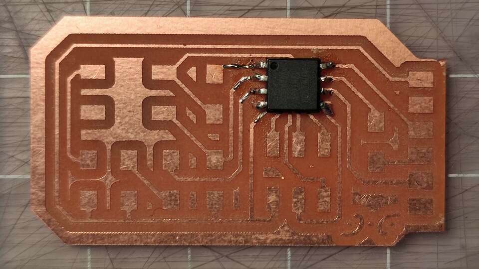
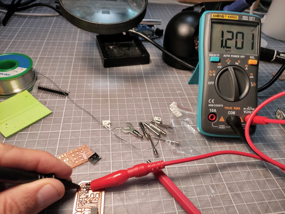
Soldering was, againg, difficult to me. I really struggled to get the AT Tiny 45 in place, and I messed up again some traces. At times, I was adding to much solder, and adjacent pins would end up connected. I did a lot of continuity testing, and finally discovered that one of the traces underneath the micro was damaged. I tried to fix it by adding a piece of wire to fix it.
Afterwards, I tried to connect it to my previously made Fab Tiny ISP, following Elena Cardiel's electronics design assignment. I really did not understand what was I doing, and when connected, all of the LEDs lit up. I do not know if they should, my guess is they should not... Anyway, I do not trust how the traces are, and since I need to practice soldering, I decided to repeat the board. I also had a look at the FTDI cable data sheet, where I found in page 12 the header Pin Out.
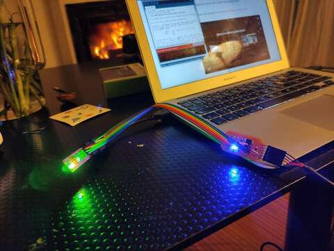
I tried to load the blink example from the Arduino IDE, but when I tried to Upload using programmer, I got the following error:
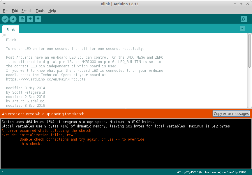
Since I am a remote student, I scheduled a meeting for the next days with one of my instructors to try to debug it, or connect the second board that I built.
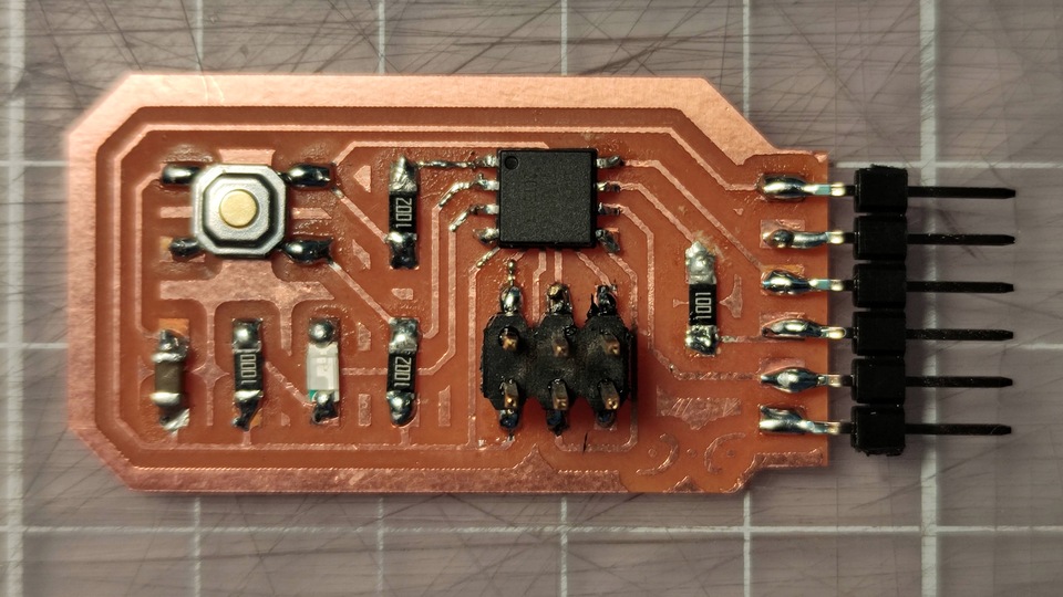
Before moving on, I reviewed Duaa's recitation on soldering, specially the tips for soldering tiny parts, and check if I was doing something wrong. I decided to replace the tip of my soldering iron, since it was kind of burnt out.
This time it worked much better. I noticed, anyhow, that the pads for the AT Tiny 45 were very small. I wouldn't definetly mind if they were a just a little bit longer... If I find how to do it, I will edit the footprint in Kicad for the next time. The rest of the board seemed easier to solder. Probably is just practice that I need...
I find soldering challenging, specially when I have my kids buzzing arround. But I have to admit that I find a sort of peace and instant reward everytime one of these tiny parts gets magically glued into its place.
Later, once I knew a little more about embedded programming, during week 09, I programmed this board, using the button as a switch. That piece of code is something that I will definetly use in my final project!
Group assignment: test equipment
In my homelab, the test equipement that I have is a multimeter and an oscilloscope. I bought them both just for the Fab Academy, and I have nerver used neither of them, so I am really looking forward to get my hands on them.
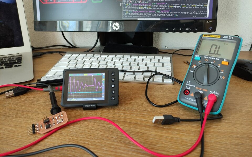
My local instructors taught me first the very basic functionality of the multimeter. The first thing I used it for was to check the LED colours, using the diode mode. In that mode, the LED will only light up if anode and cathode are connected in the right way. The next mode was the continuity check, that beeps when there is a closed circuit. Later, I tested some resistors, and finally some capacitors.
As for the oscilloscope, this was just a brief intro to it. It is a Seed Studio nano v3, with just one channel, but I guess it will be good enough for my needs as I am completely new to this field. The specs says that it has 6 triggering modes, built-in signal generator and 200kHz analog bandwidth. Honestly, I am not sure what those mean yet... Anyhow, using it is quite straightforward, just connect the black probe to ground and the white probe to the signal to measure. It mainly measures volts, and for now I just saw how it varied when I turned the LED on and off.
During the final project development, I did use much more the oscilloscope, when debugging the functioning of the h-bridges, using software PWM.