7. Electronics design
Reguirements
group project
use the test equipment in your lab to observe the operation of a microcontroller circuit board
Our Group members: Anssi, Achille, Jari and me. This weeks group project documentation is in Achille’s site
individual project
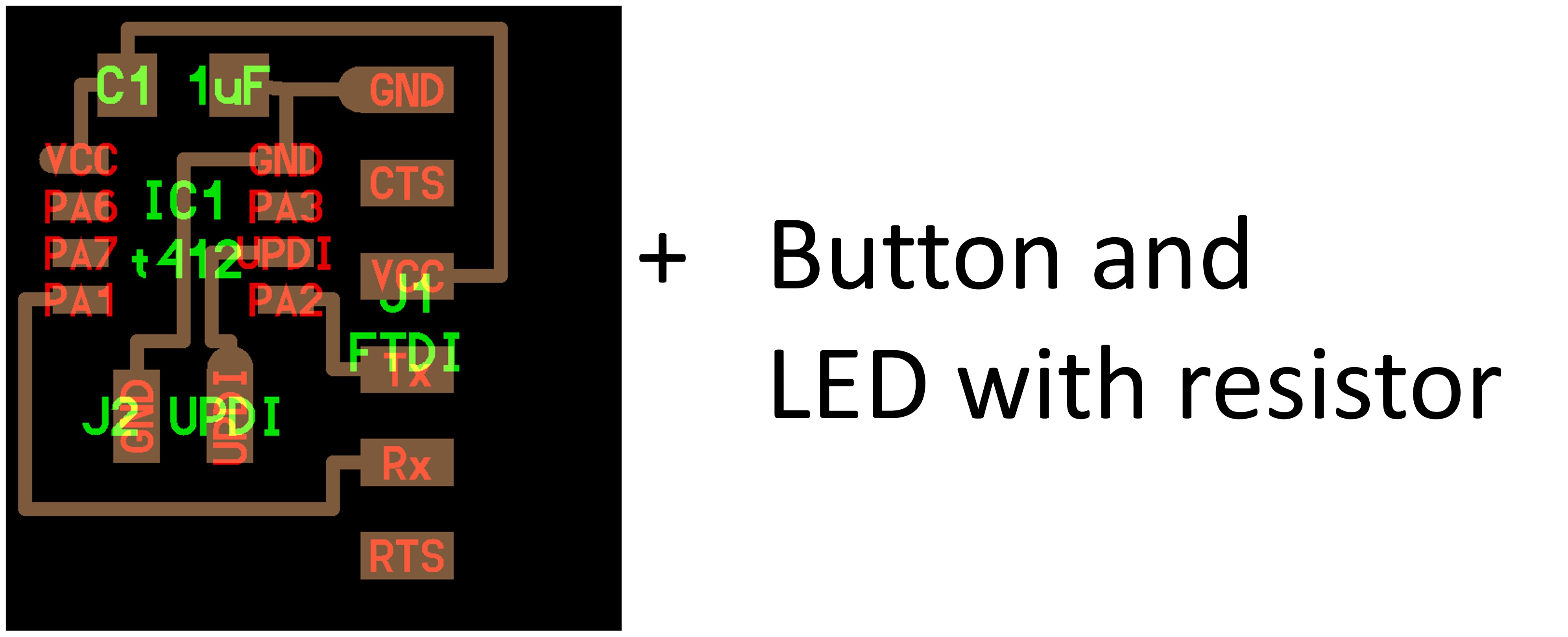
redraw an echo hello-world board, add (at least) a button and LED (with current-limiting resistor) check the design rules, make it, and test it extra credit: simulate its operation
individual project
Research
First got echo hello-world board desing data but I have to note requiremets (add (at least) a button and LED). So, I have to add button and LED to board. Our hello-world board based on ATtiny212/412 microcontroller. I will use my new programmer to program my echo hello-world board.
I found good template for my projet. Antti Rytilahti has ready made schema in his page Antti Rytilahti schematic-editor
I used in Electronics production week Autodesk Eagle, but now I decided to use KiCad to design my new PCB.
Plan to work flow
KiCad install and Fab Lab settings 1. Downloading installing programm 2. Installing of KiCad 3. Fab Lab settings 4 Design of PCB 1. Create a schematic 2. Create a layout 3. Create the actual PCB 4. Production of PCB 1. Milling data 2. Cut 3. Milling Soldering Programming Testing
KiCad install and Fab Lab settings
Installing process
Step 1. I went KiCad home page. There I found download button for downloading.
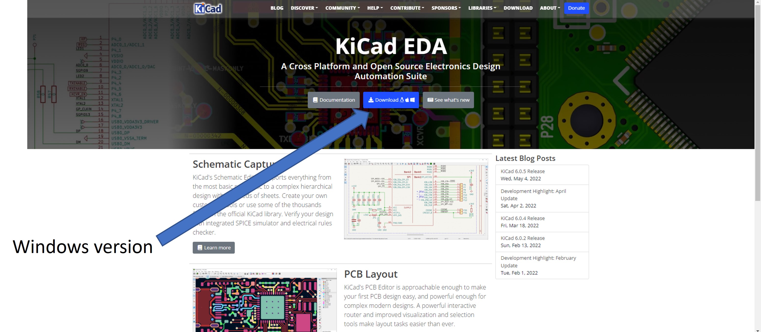
Step 2. I saved kicad-6.0.2-x86_64.exe to my PC
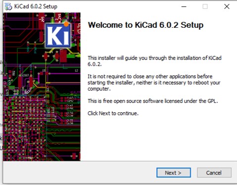
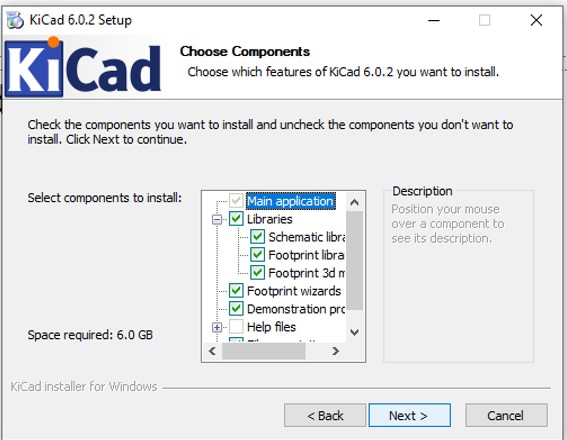
Step 3. I started installing process to start kicad-6.0.2-x86_64.exe. I did not changed componets selections. Default selections was OK for me.
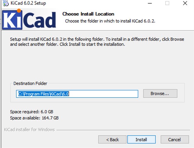
Step 4. I set destinatin Folder for KiCad program
Step 5. Then installing started
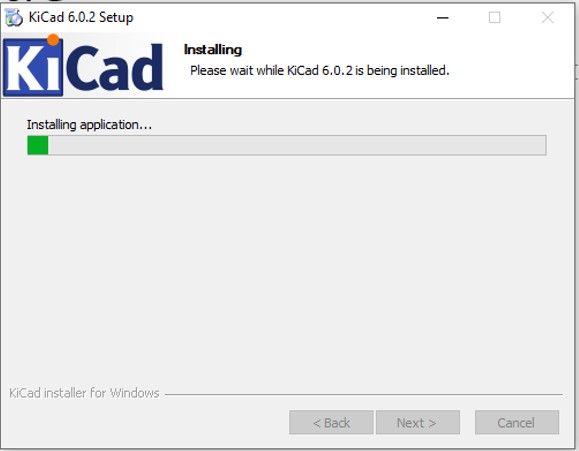
Step 6. Installing took time, but at last installing was at the end.
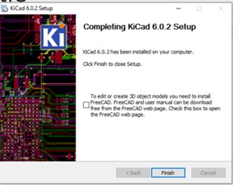
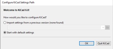
Step 7. At last I konfigured KiCad to start with default settings
Fab Lab settings
After installing it is necessary to included Fab Lab’s components libraries and footprints to KiCad.
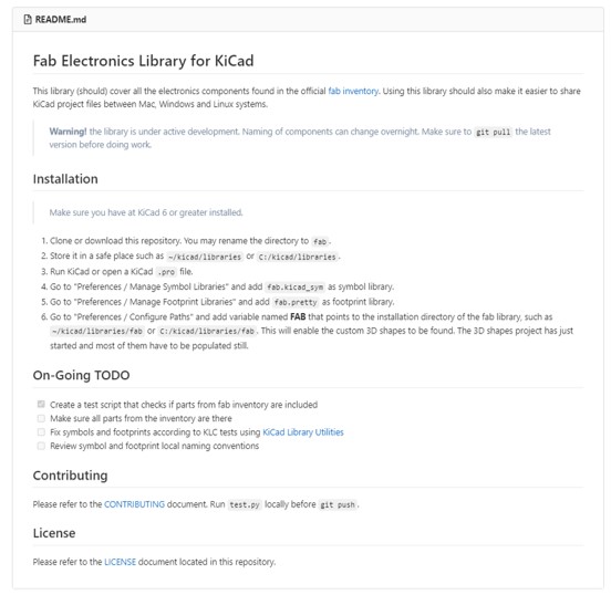
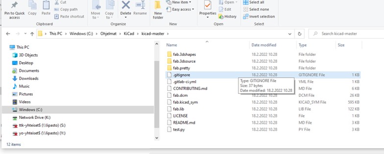
Step 1. I went Gitlab to download libraries. Address is https://gitlab.fabcloud.org/pub/libraries/electronics/kicad
There are good instruction to install libraries. I followed that in next steps
Step 2. I pushed download icon. Then popup menu appeared.
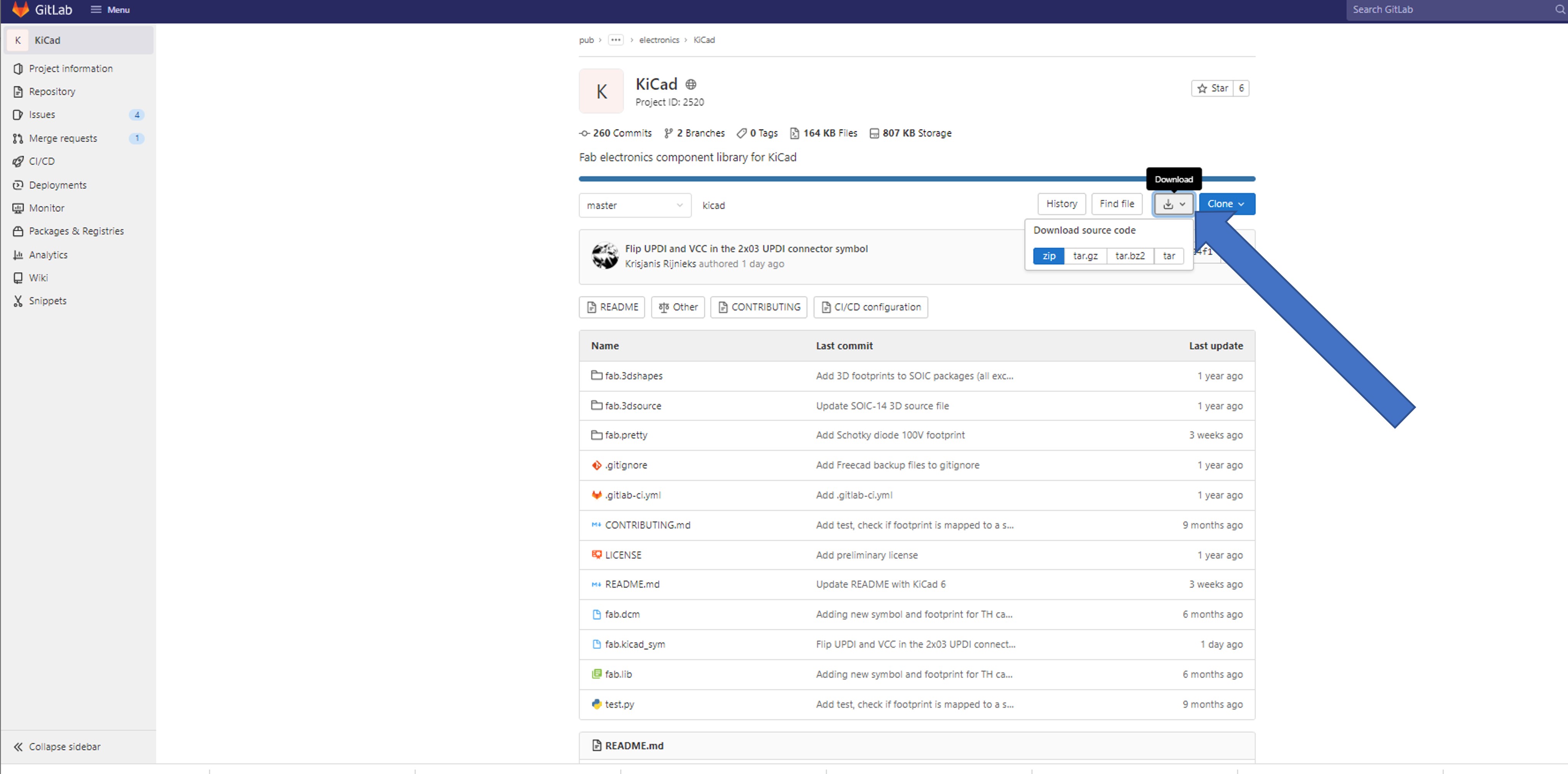
Step 3. I downloaded repository in Zip format (Compressed Folder) to my PC
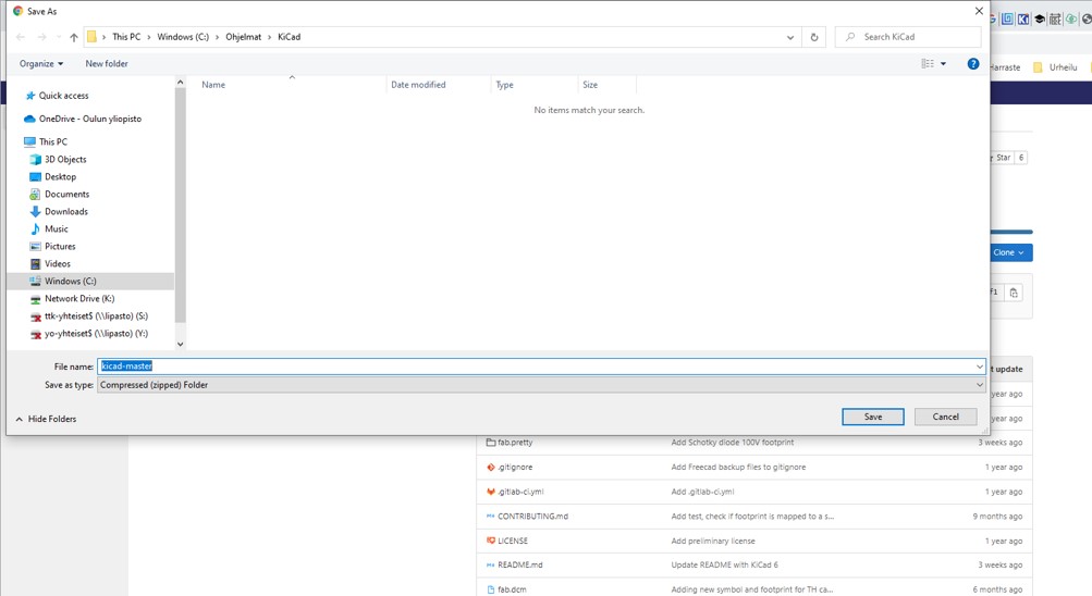
Step 4. Then I Unzipped Zip (Compressed Folder) to KiCad folder
Step 5. I opened KiCad. I selected Preferences and then Configure Paths…
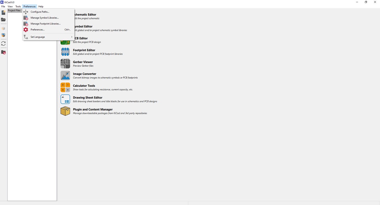
Step 6. Then popup menu appeared.
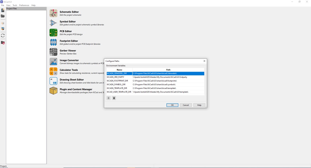
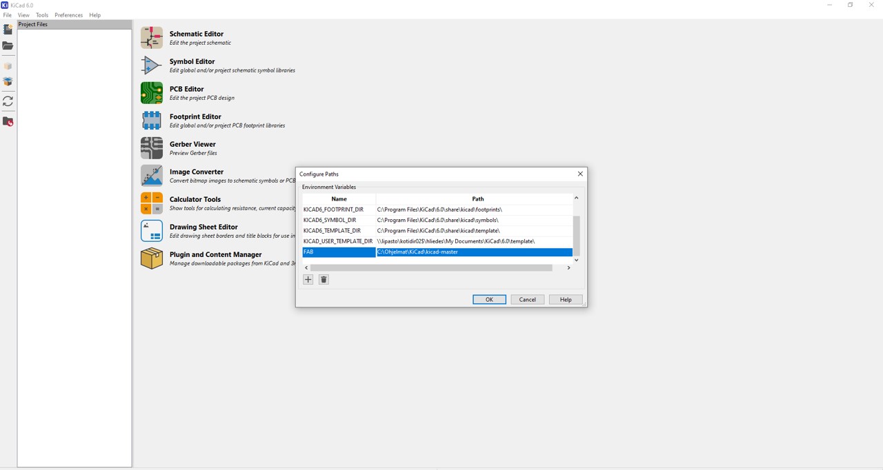
Step 7. I clicked plus mark to add new line to FAB
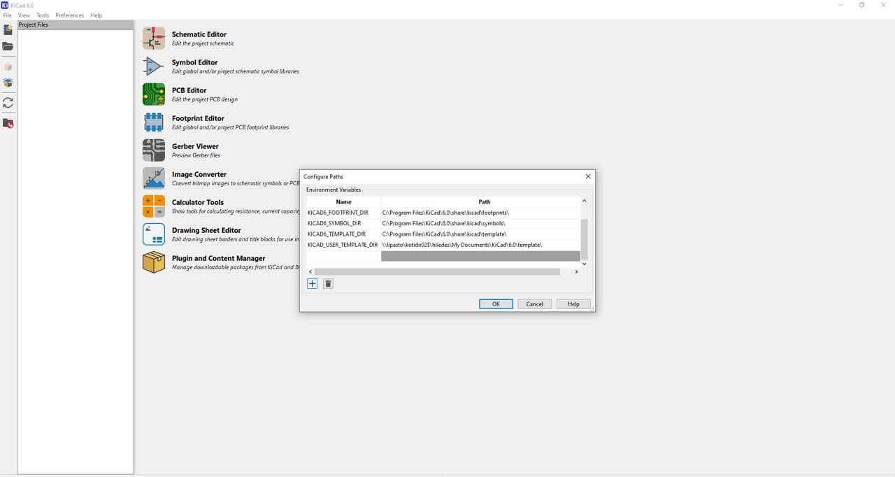
Step 8. Then I selected to Path Kicad-master folder
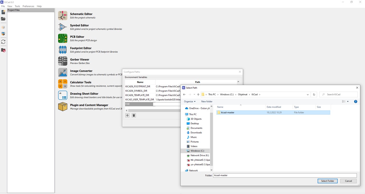
Step 9. Now there are new line to FAB Kicad-master
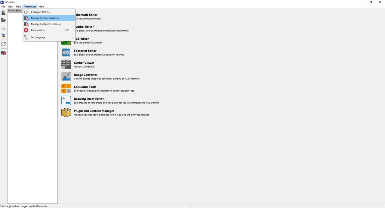
Step 10. Then I selected Preferences and then Manage Symbol Libraries…
Step 11. Then popup menu appeared to choose Global Symbol Table. I selected default value (Copy default global symbol library table) and pushed OK button.

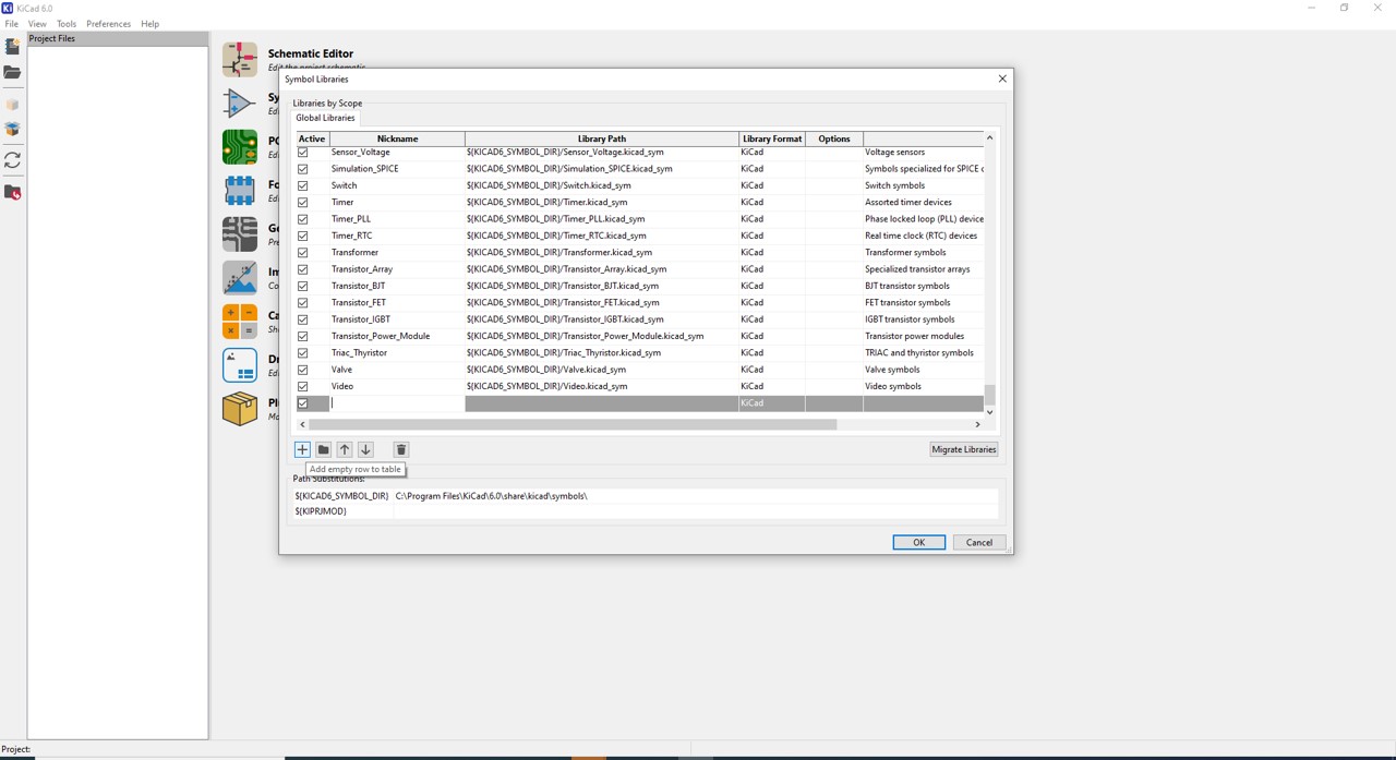
Step 12. Then popup Symbol Libraries table appeared
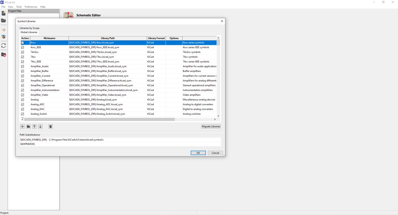
Step 13. I clicked plus mark to add new line to fab.lib
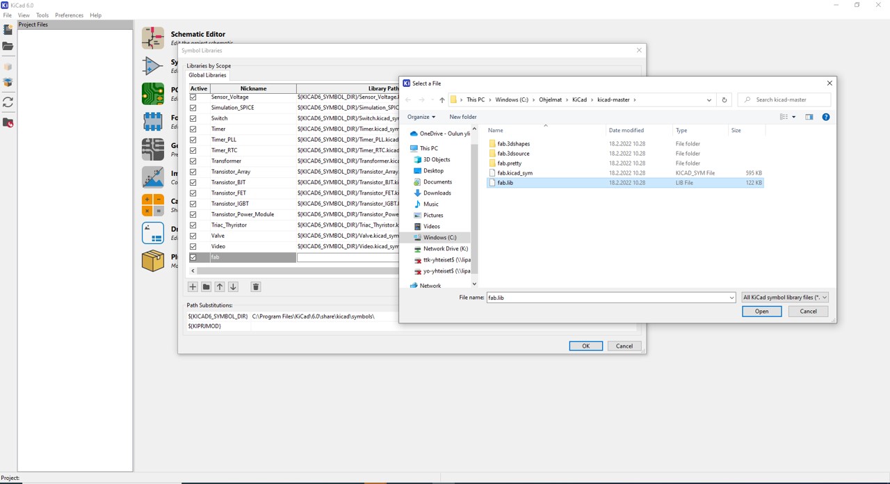
Step 14. I selected fab.lib file from Kicad-master folder
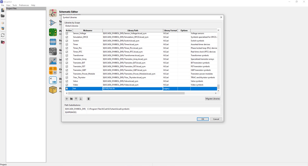
Step 15. Now there are new line to fab.lib file
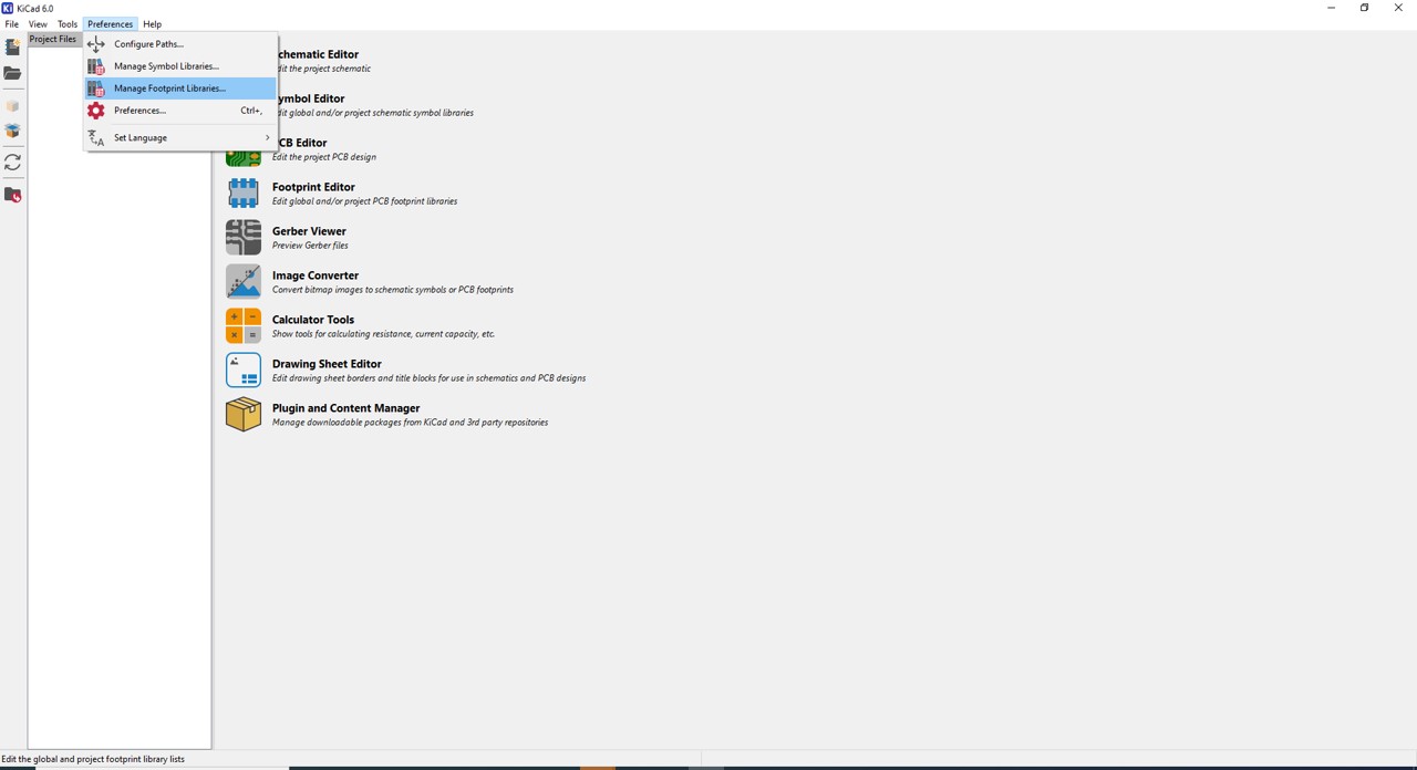
Step 16. Then I selected Preferences and then Manage Footprint Libraries…
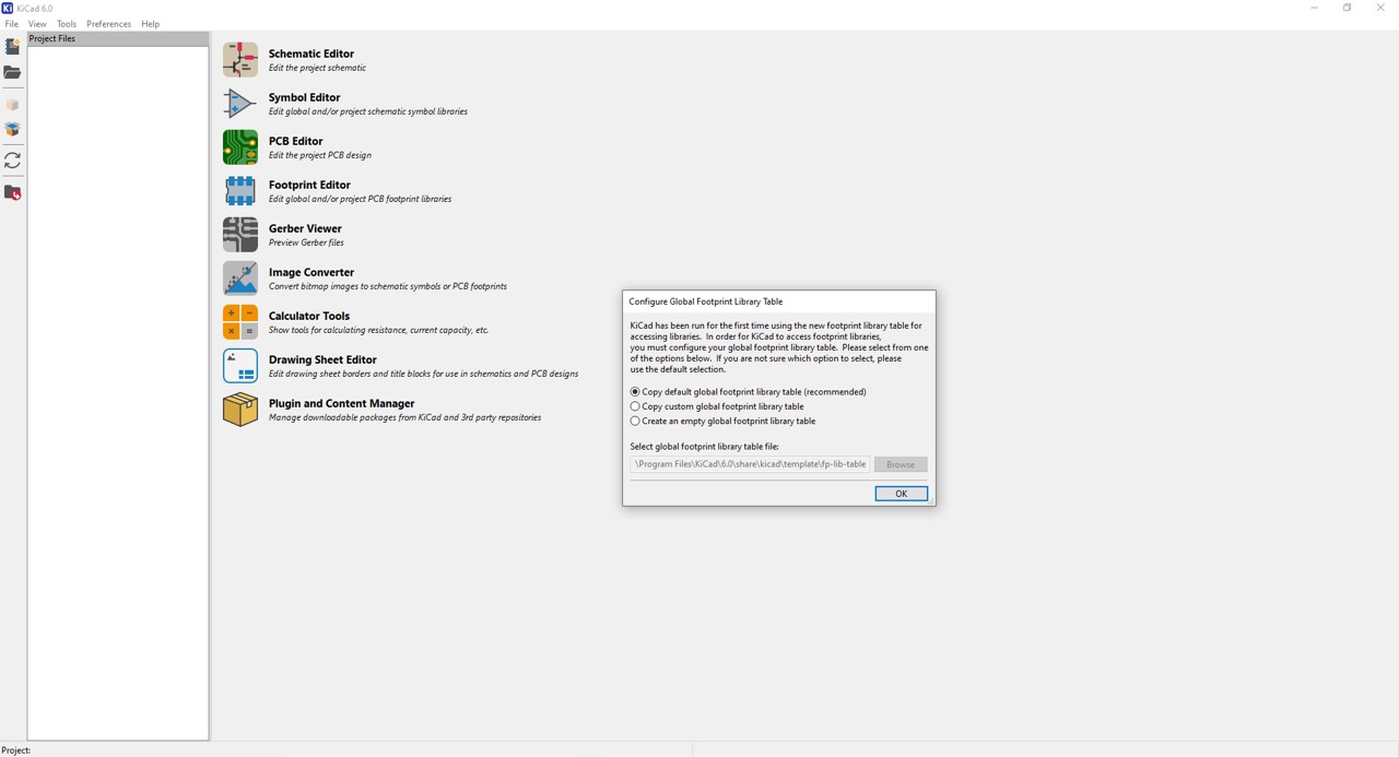
Step 17. Then popup Global Footprint Library table appeared. I selected default value (Copy default global footprint library table) and pushed OK button.
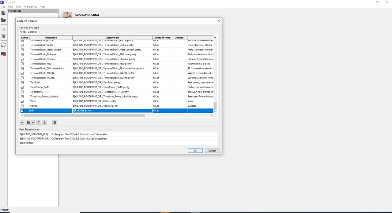
Step 18. Now there are new line to fab.pretty
Design of PCB
Start new project
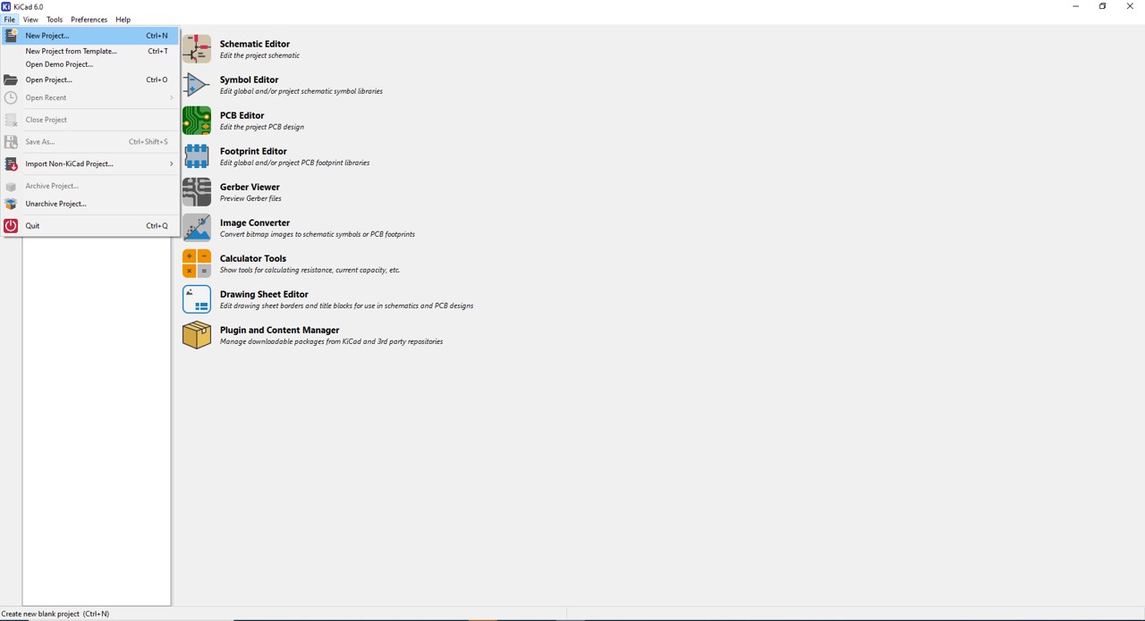
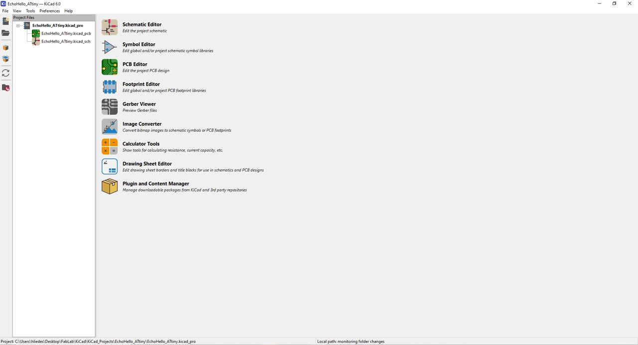
Step 1. I selected File and then New Projet…
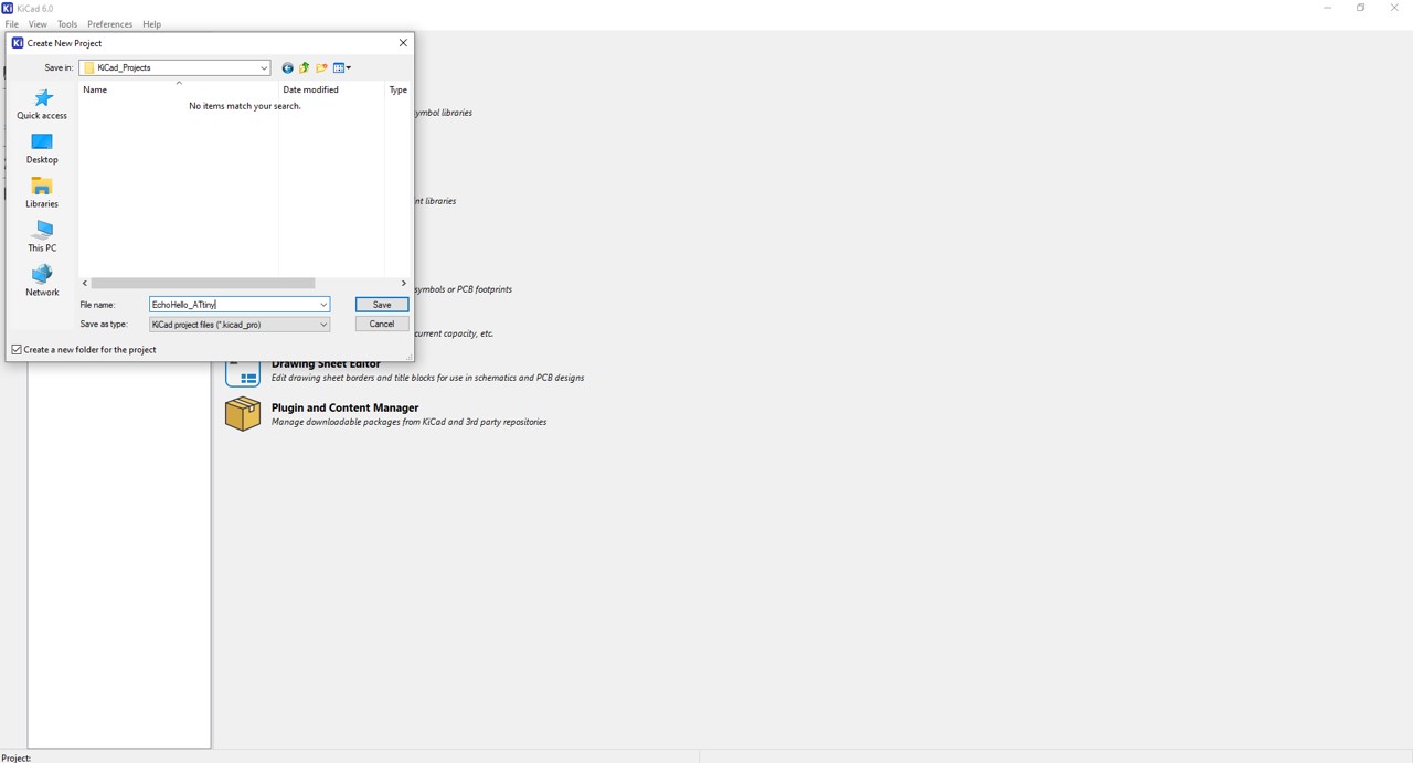
Step 2. Then popup Menu appeared to give name and select folders new project. I gave name EchoHello_ATiny
Step 3. After that project have EchoHello_ATiny.kicad_pcb and EchoHello_ATiny.kicad_sch parts
Schematic design - Schematic Editor
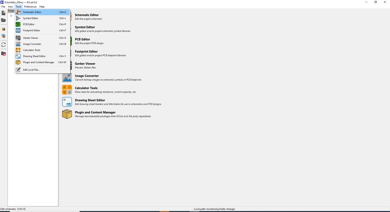
Step 1. I selected Tools and then New Projet…
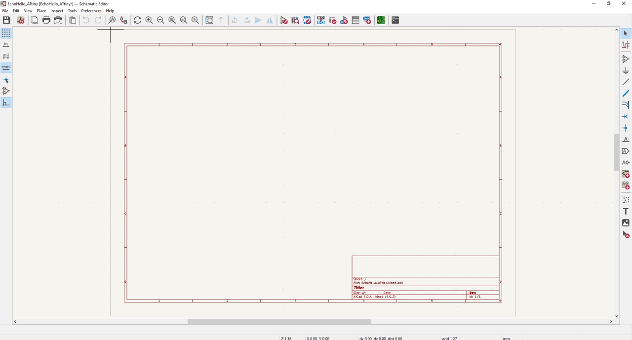
Step 2. Then new Sheet appeared
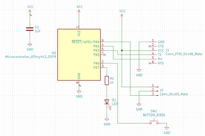
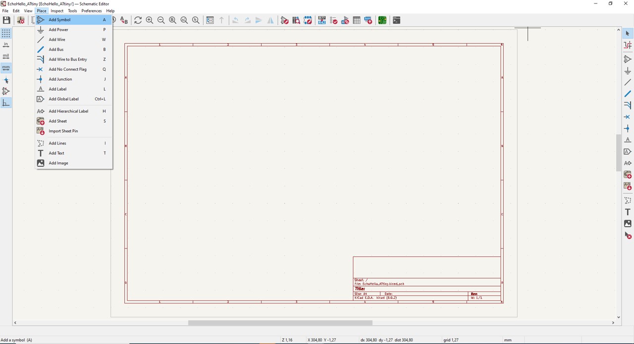
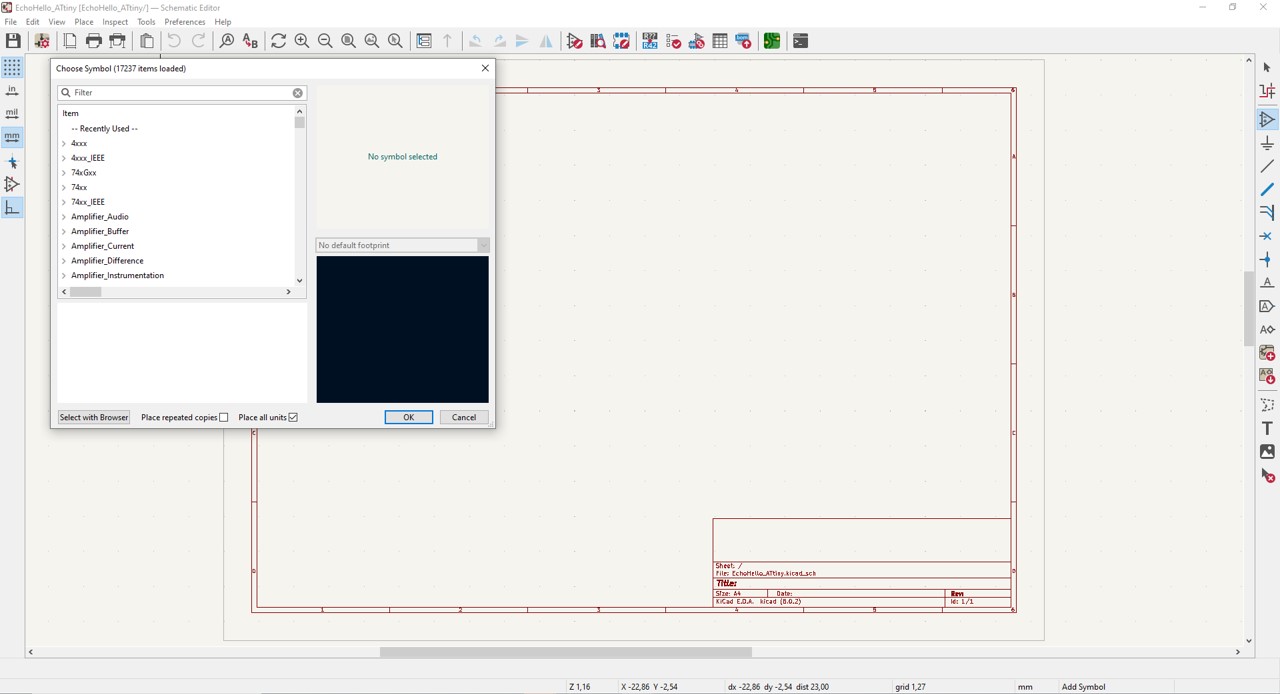
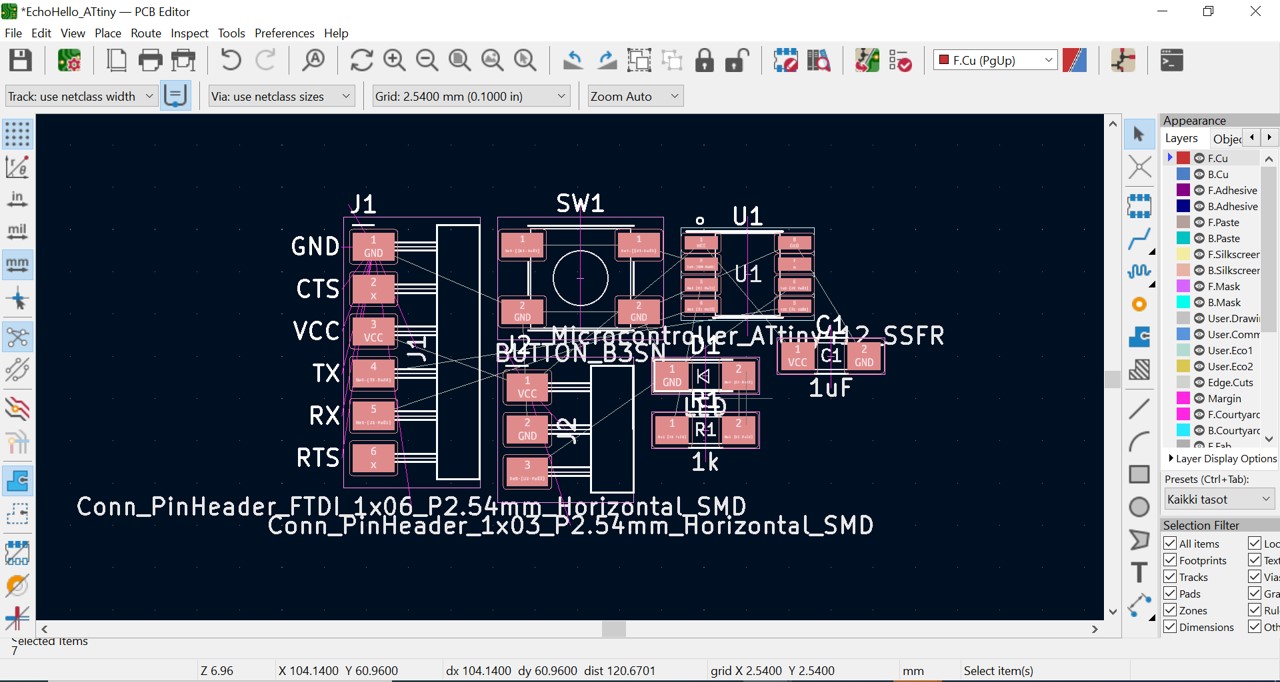
Step 3. I started to add components to sheet - Place/Add symbol. First I added Microcotroller.
Step 4. Then new menu appeared. I typed to filter field “fab att”.
Step 5. Then I got list. I selected “Microcontroller_ATtiny412_SSFR”
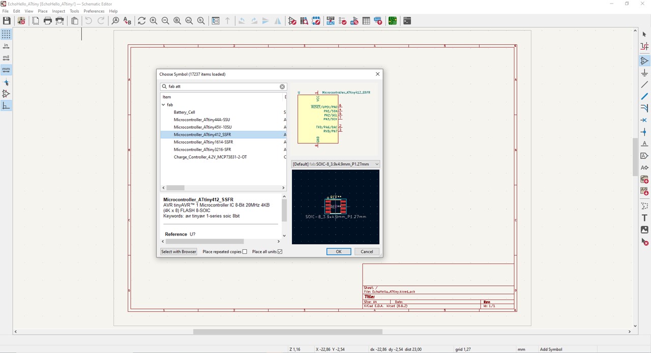
Step 6. Then selected component appeared to Sheet.
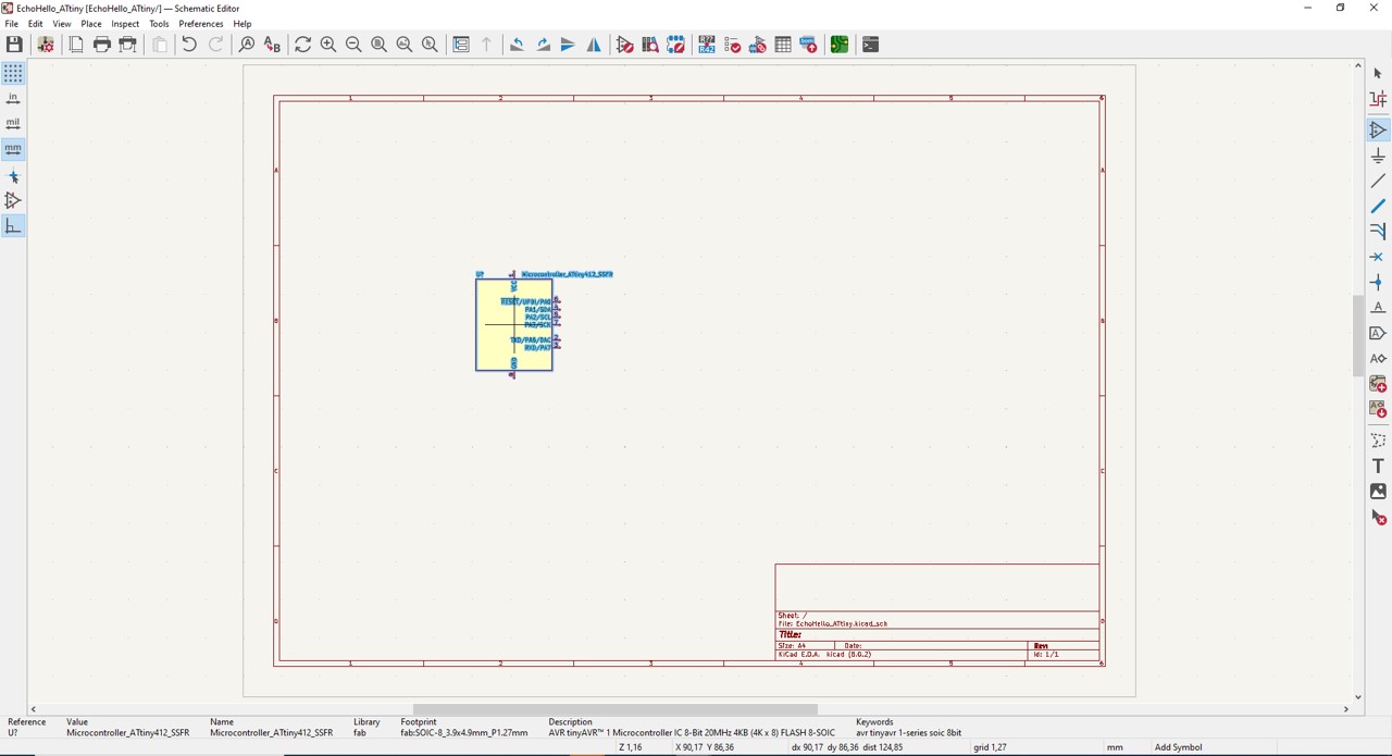
I added rest of components and symbols (Grd and Vcc) to sheet in the same way (Steps 4, 5 and 6)
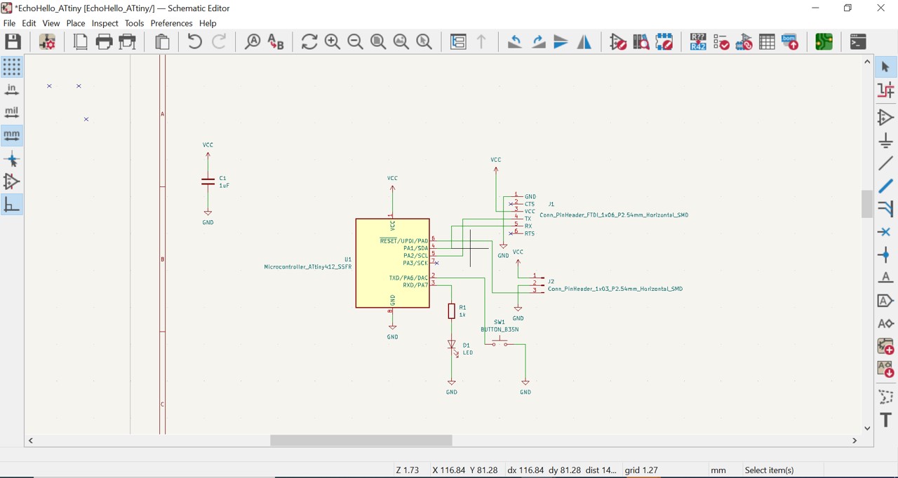
These components and symbols are needed to insert to sheet - ATtiny412 (Main IC) - C (Capacitor) - R (Resistor) - BUTTON_B3SN (Push bottun, OMRON) - LED (LED) - Conn_FTDI_01x06_Male (6pin connector for FTDI) - Conn_01x03_Male (3pin connector for serial&power) - VCC - GND
Note! You can use hotkey to rotate (“R”) components
Step 7. Then all components and symbols were on sheet. I got a idea add pictures of template and components list to sheet.
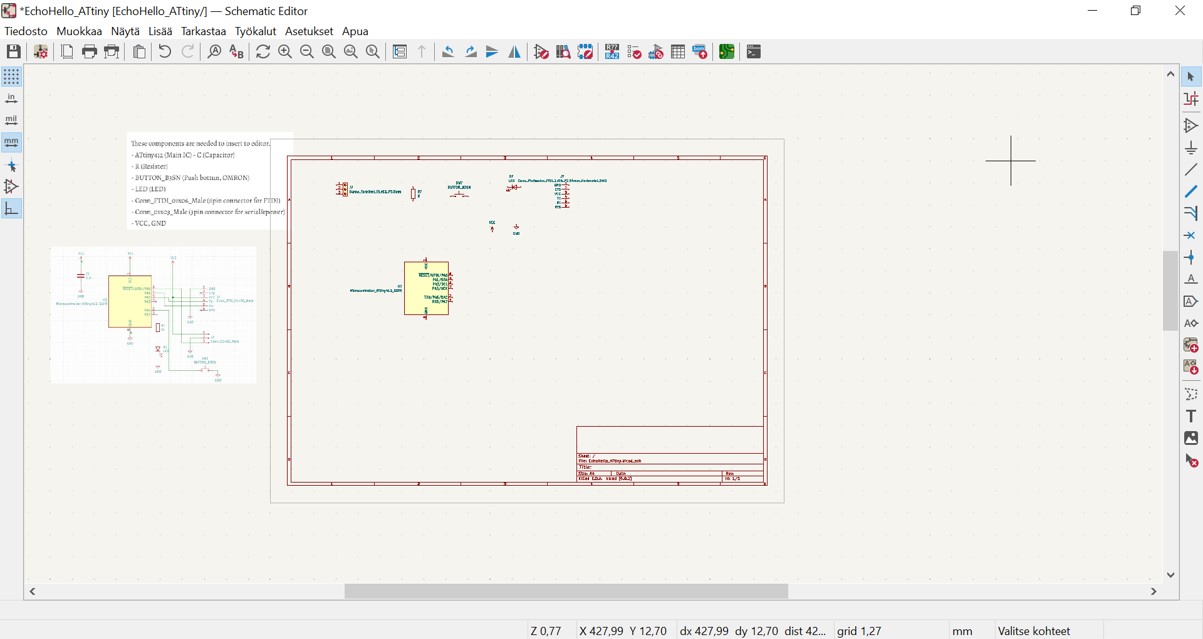
I connected components and symbols wires tool by hotkey “w”.
Then I started to give values to components.
Step 8. I clicked component and then I pushed hotkey “v” to open value menu.
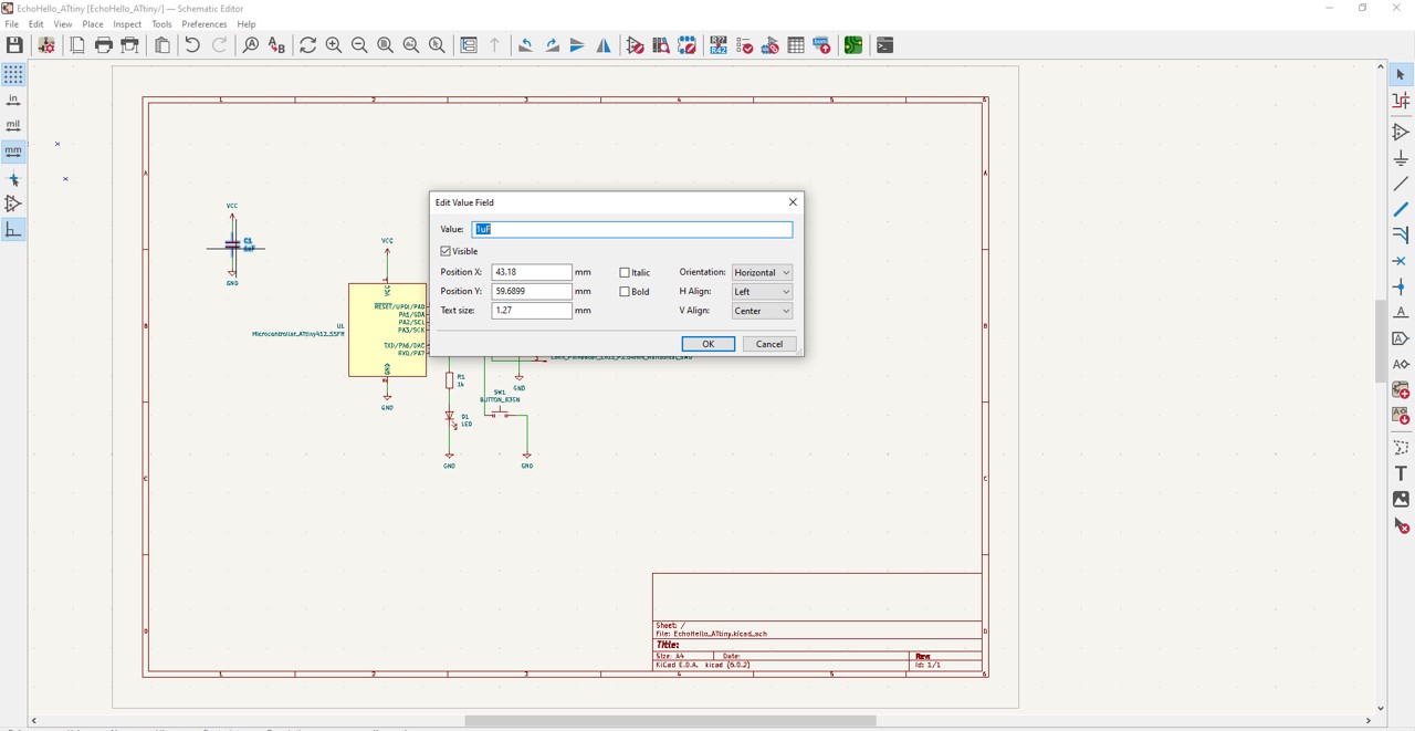
I added rest of values to components in the same way (Step 8 ).
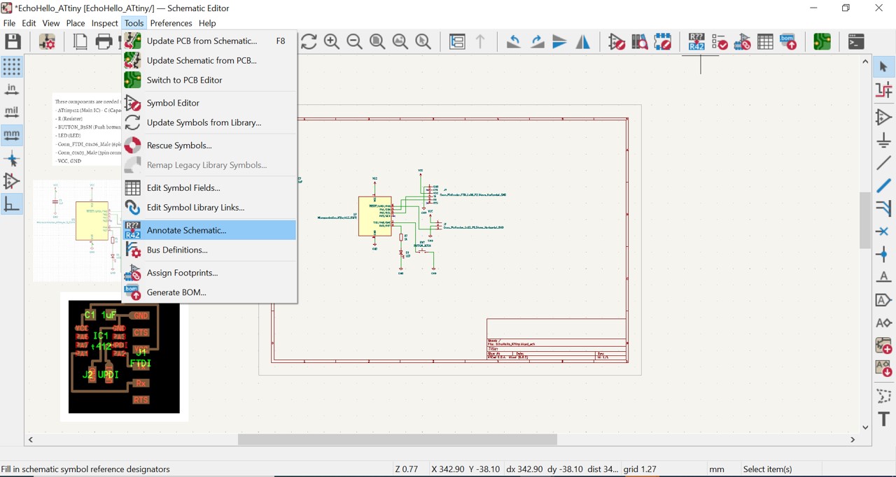
Now all components were values, but not numbers. I ran Annotate Schematic to number components
Step 9. I clicked Tools and then Annotate Schematic…
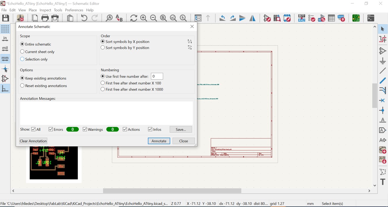
Step 10. Then Annotate Schematic menu appeared. Defaults values were ok. I pushed Annotate button.
Step 11. Then Annotate messages appeared. I pushed Close button.
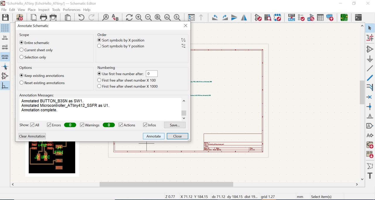
Step 12. After that components got number values.
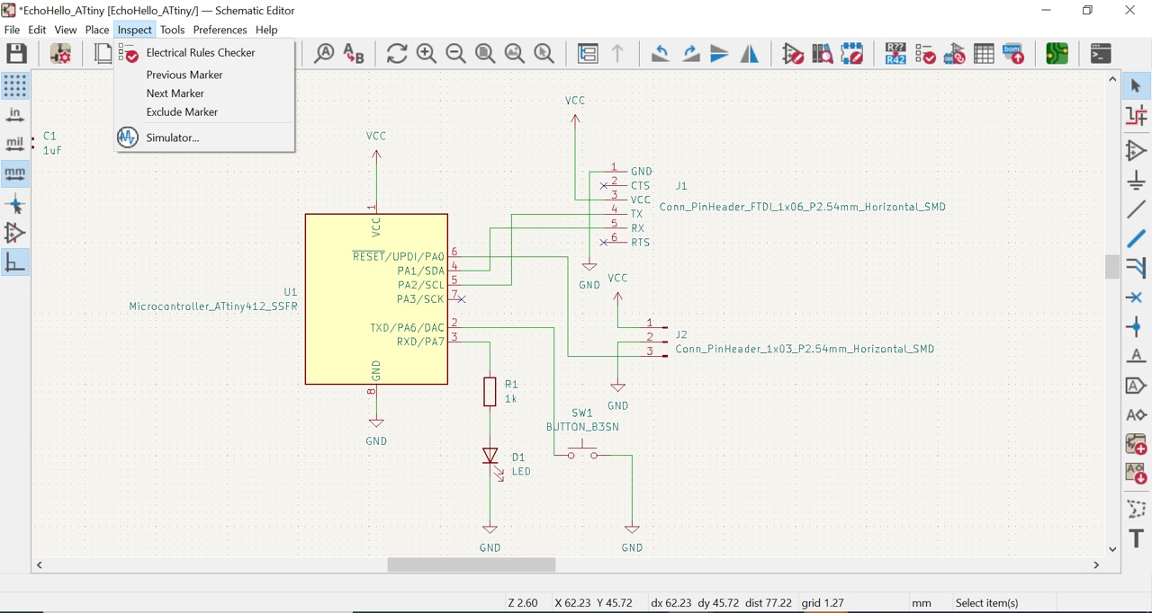
Next I checked electrial rules
Step 13. I clicked Inspect and then Electrial Rules Checker
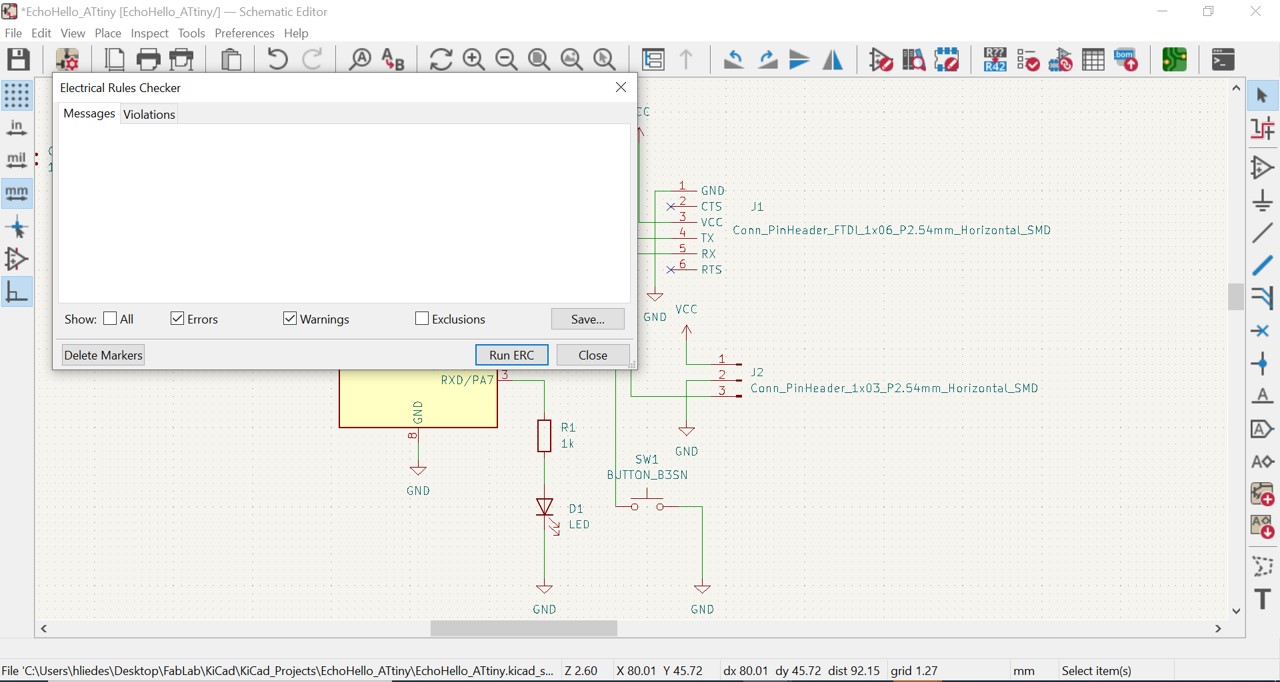
Step 14. Then Annotate Electrial Rules Checker menu appeared. I pushed Run ERC button.
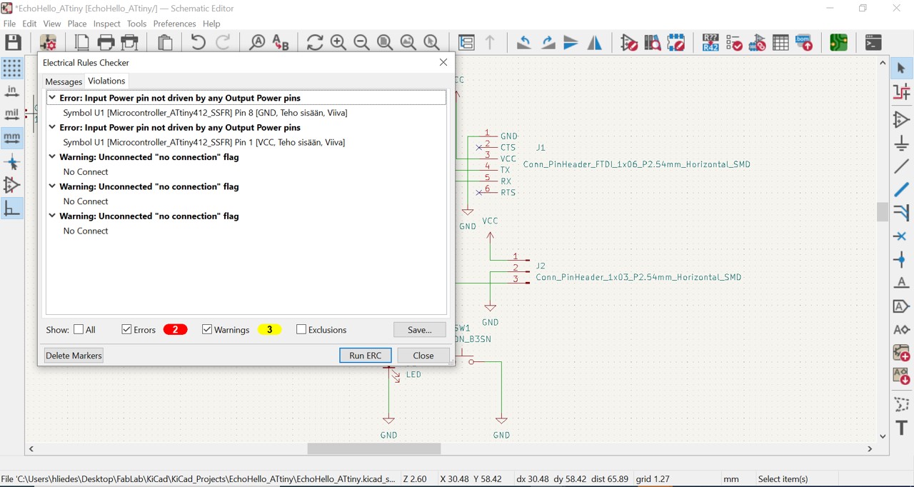
Step 15. Checking gave some errors and warnings. I checked errors and warnings and fixed them
Then I checked footprints
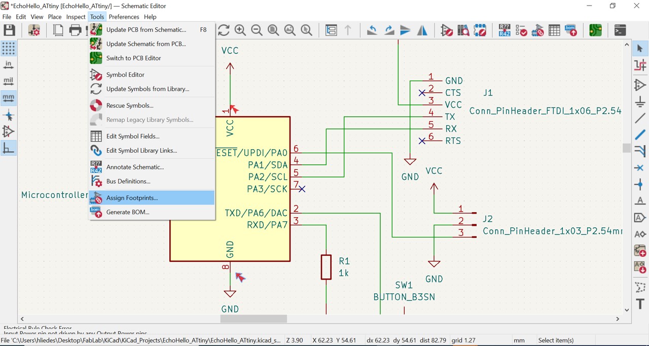
Step 16. I clicked Tools and then Assign Footprints…
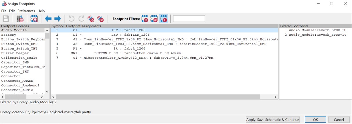
Step 17. Then Assign Footprints menu appeared. I checked that all components had footprints. I clicked first line “1C11uF:fab:c_1206”
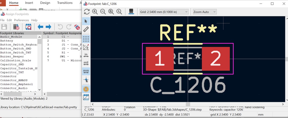
Step 18. Then Footprint picture of component appeared.
PCB design
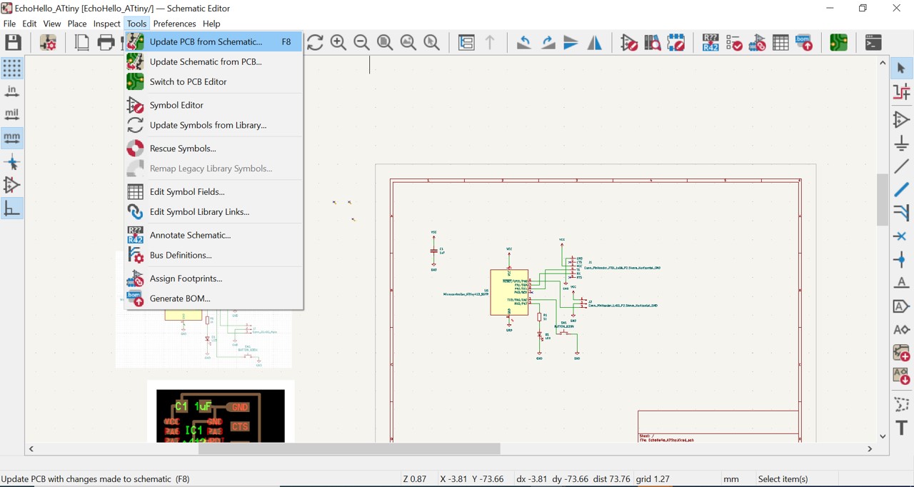
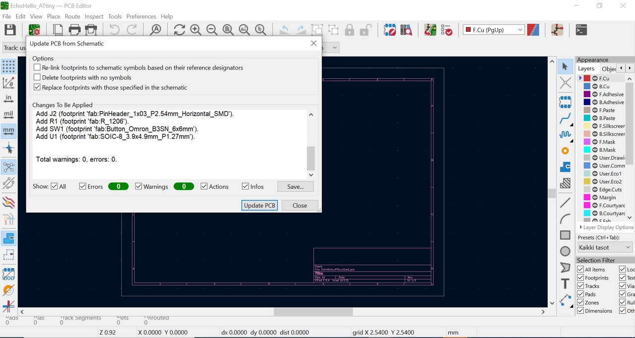
Step 19. To start PCB design I clicked Tools and then Update PCB from Schematic…
Step 20. Then Update PCB from Schematic menu appeared. I pushed Update PCB button.
Step 21. And next I pushed Close button.
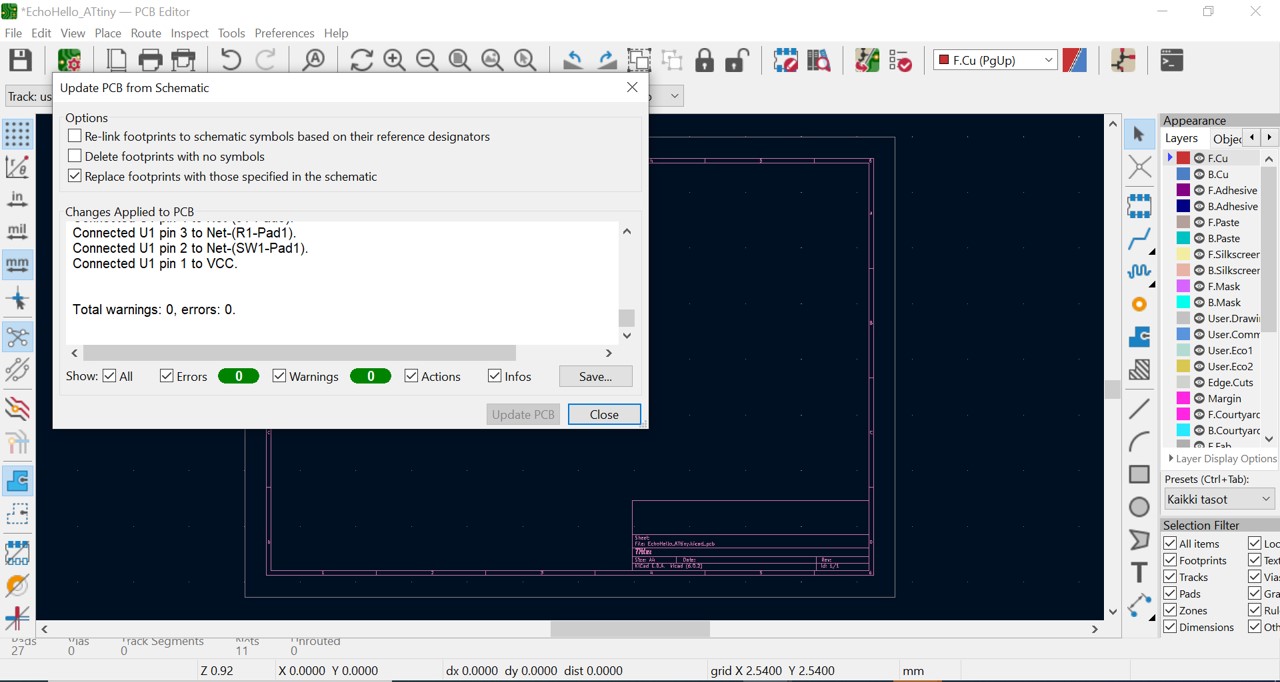
Step 22. All components appeared onto PCB
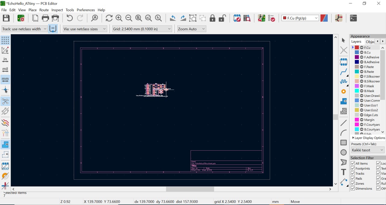
Step 23. I zoomed view
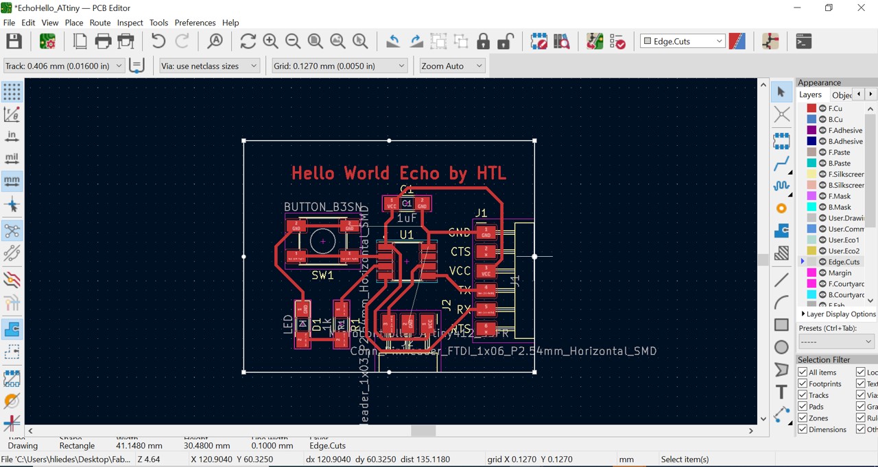
Step 24. I placed and rotated components to right positions
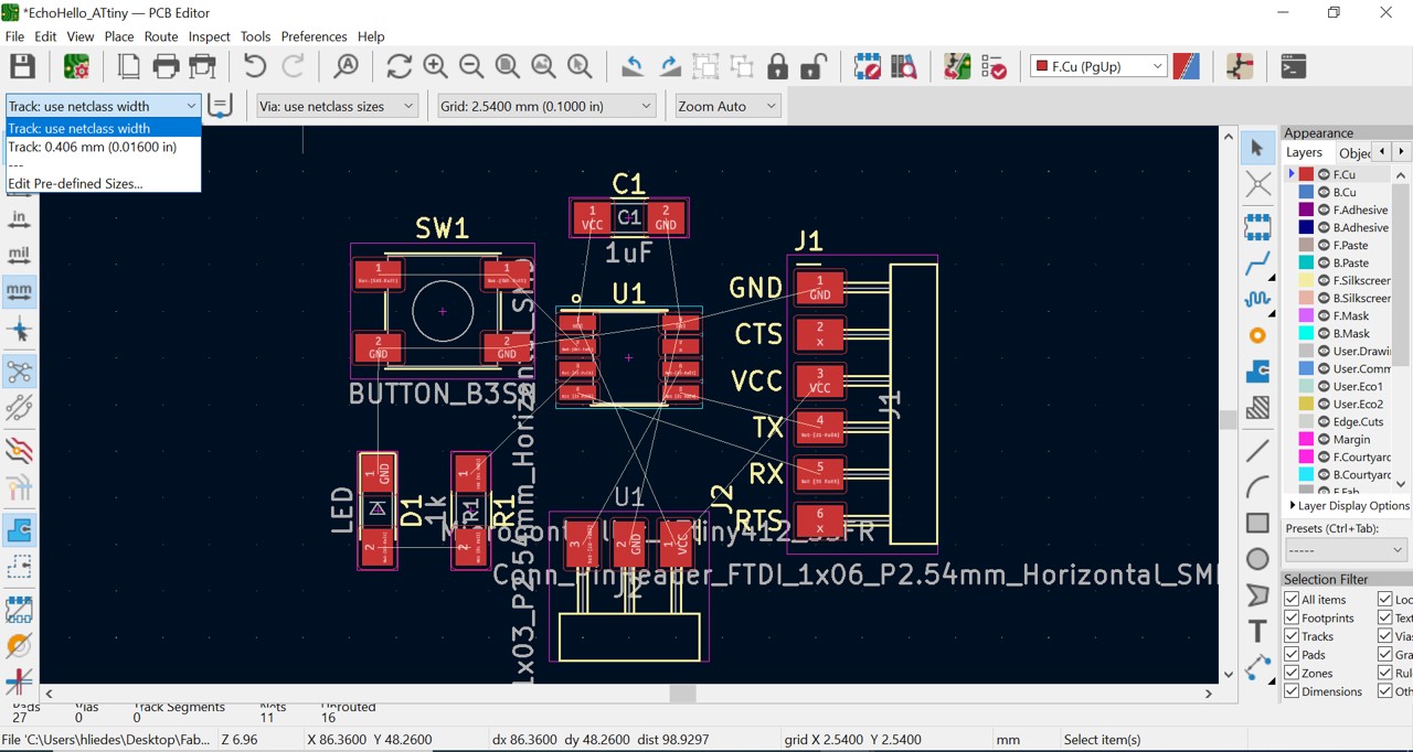
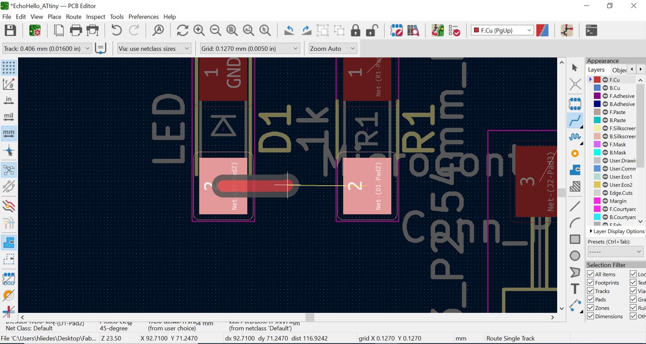
Step 25. Then I connected all the wires except Gnd.
Step 26. Then I added text “Hello World Echo by HTL”
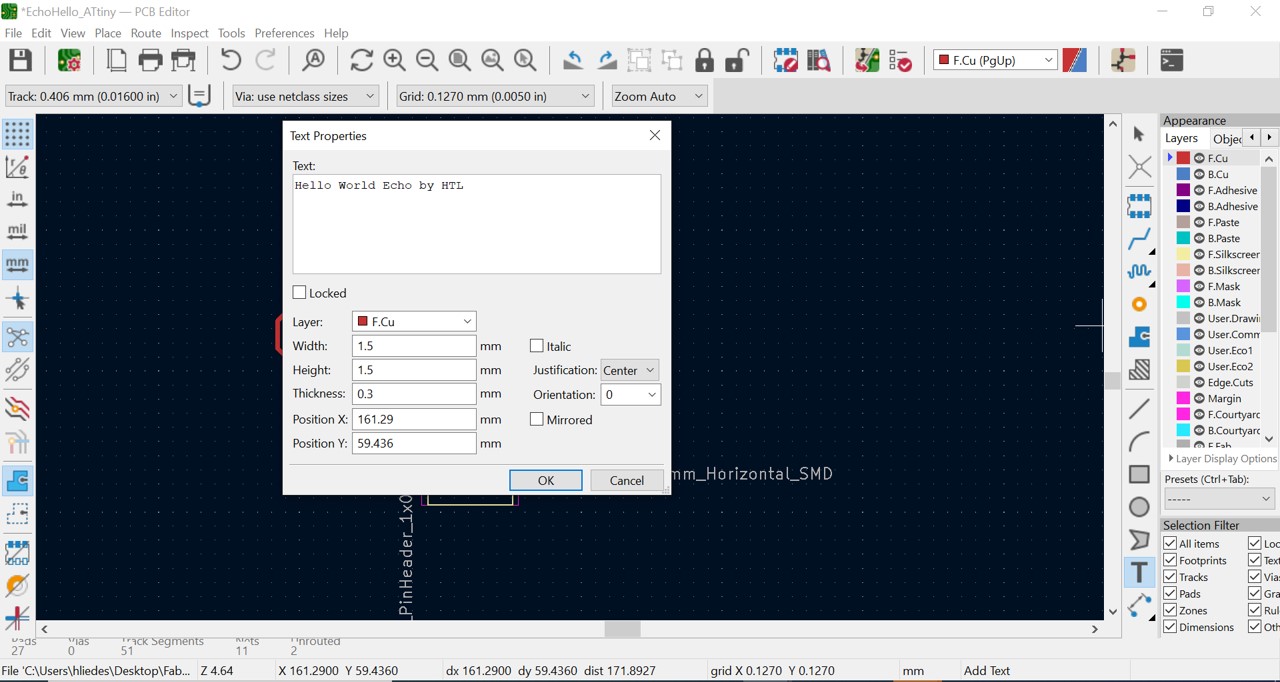
Step 27. I placed the text to right positions
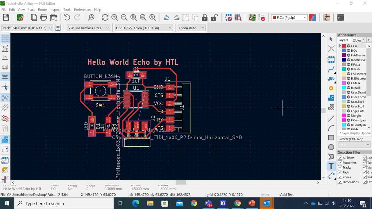
Step 28. Then I drawed Edge Cut
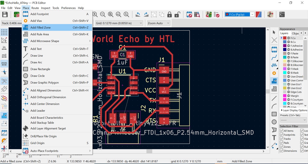
Then I addedd Ground area
Step 29. I clicked Place and then Add Filled Zone
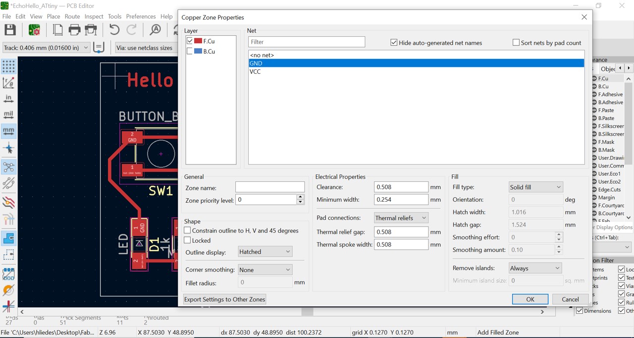
Step 30. Then Copper Zone Properties menu appeared. I clicked OK button
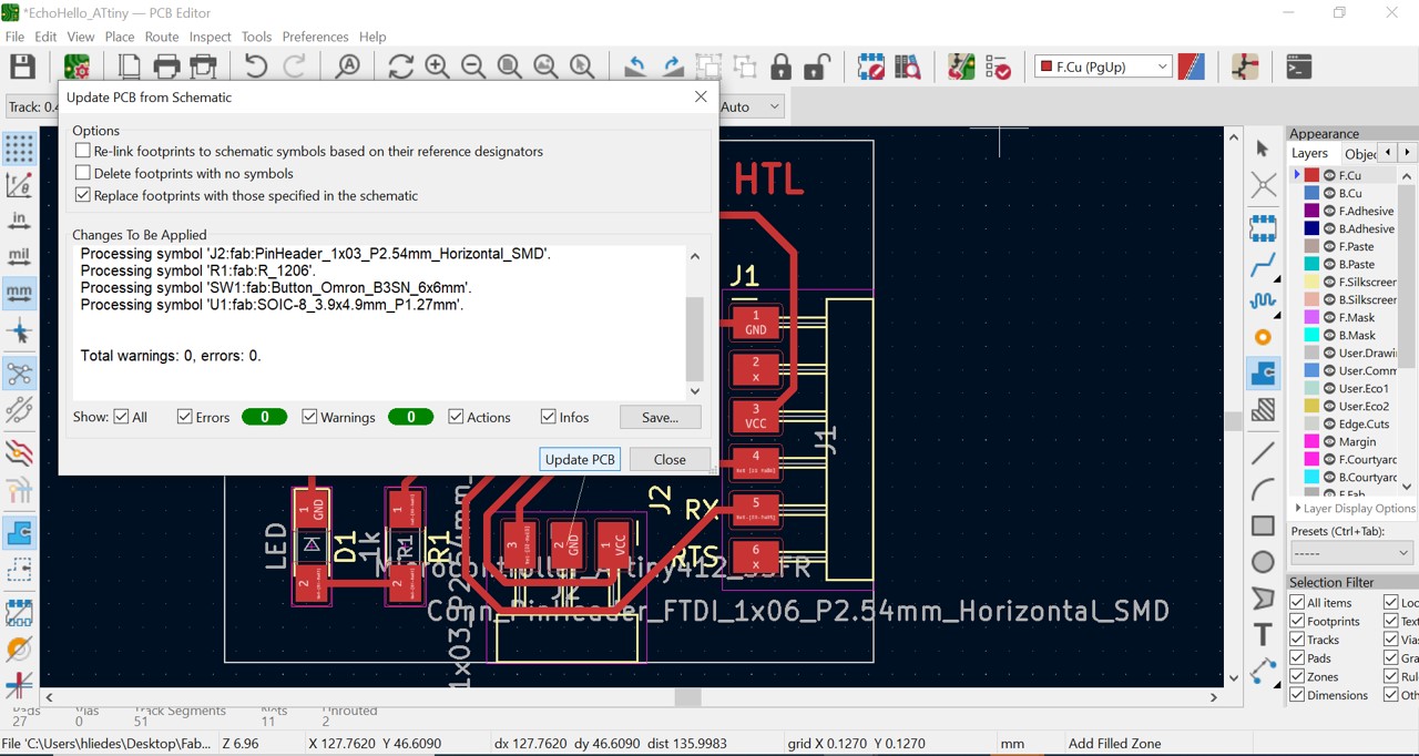
Step 31. Then Update PCB from Schematic menu appeared. I clicked Update PCB button
Step 32. Now my PCB was ready
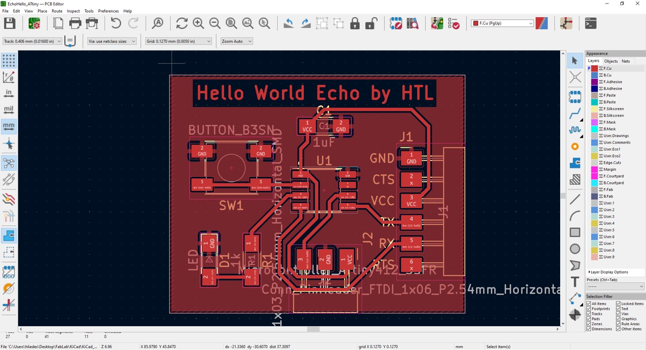
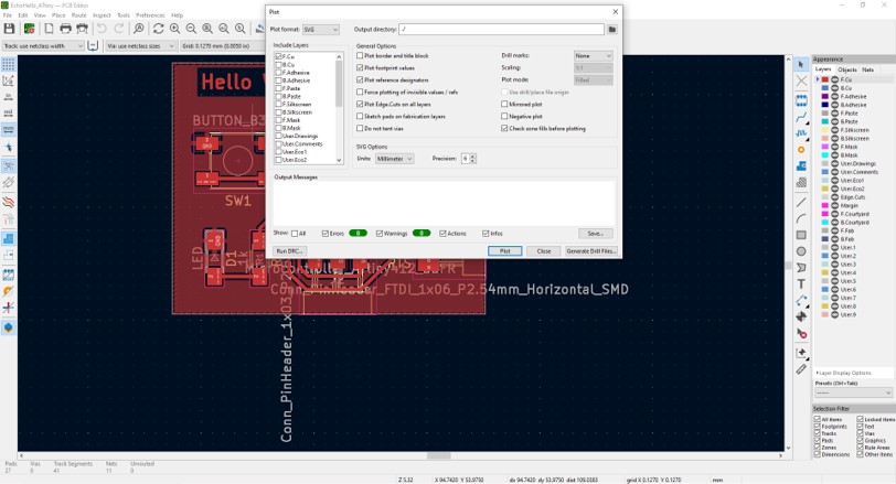
At finally I plot milling files
Step 33. I File and then Plot…
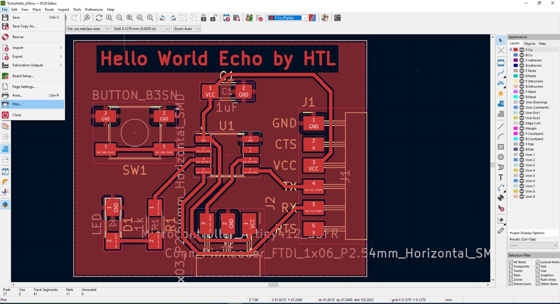
Step 34. Then Plot menu appeared.
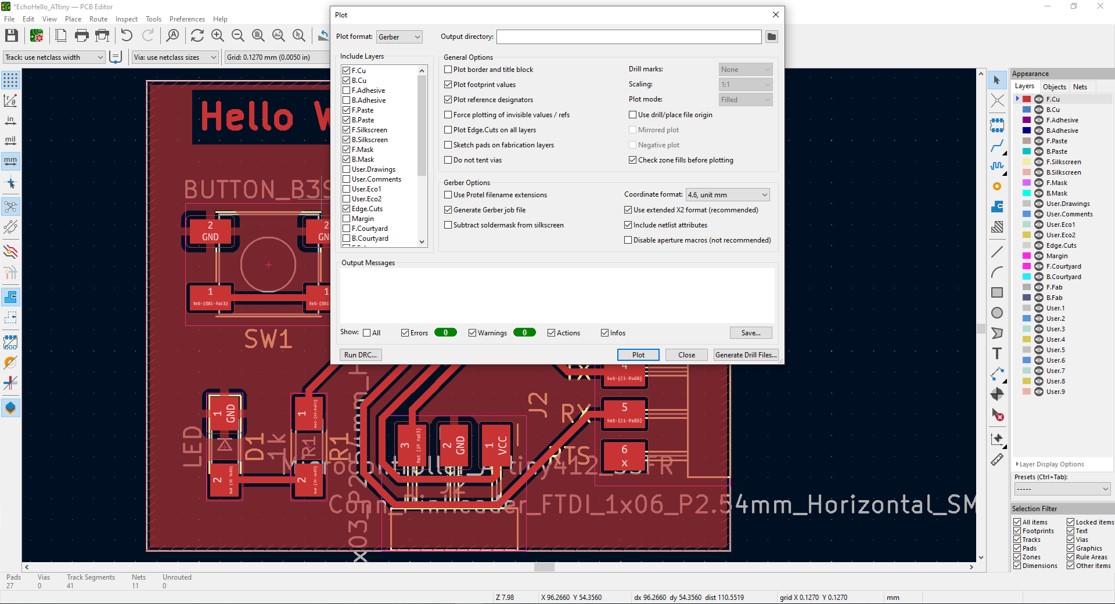
Step 35. I choosed Plot format: Gerber, Include Layers: F.Cu, Edge.Cuts
I clicked Plot button
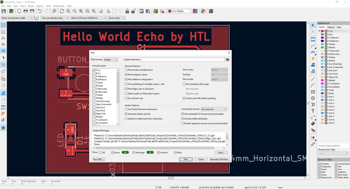
Step 36. At last I got gerber files to milling.
Step 37. I also saved Plot format: SVG, Include Layers: F.Cu, Edge.Cuts
I clicked Plot button
Production of PCB and programming
I have documented PCB manufacturing and echo hello board programming processes in week 5. Electronics productions.
Testing
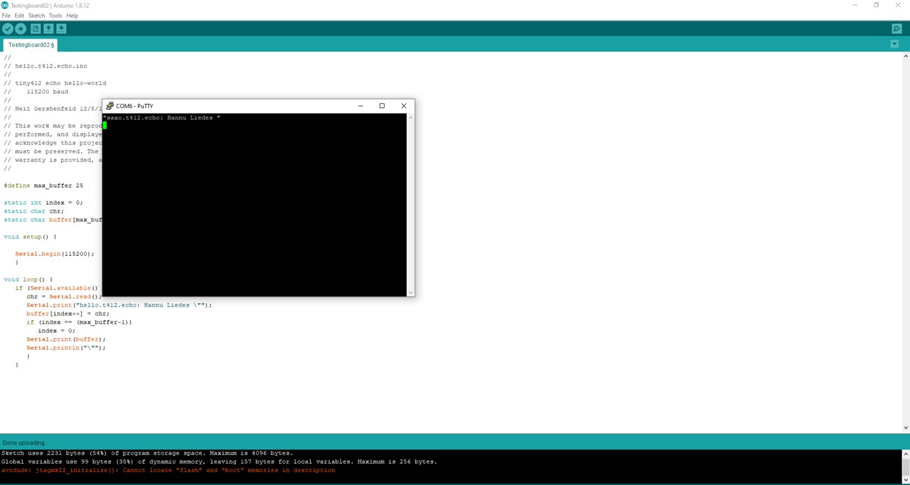
Step 1. I connected the board to my programmer
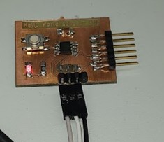
Step 2. I uploaded echo program to Echo board. It works fine.
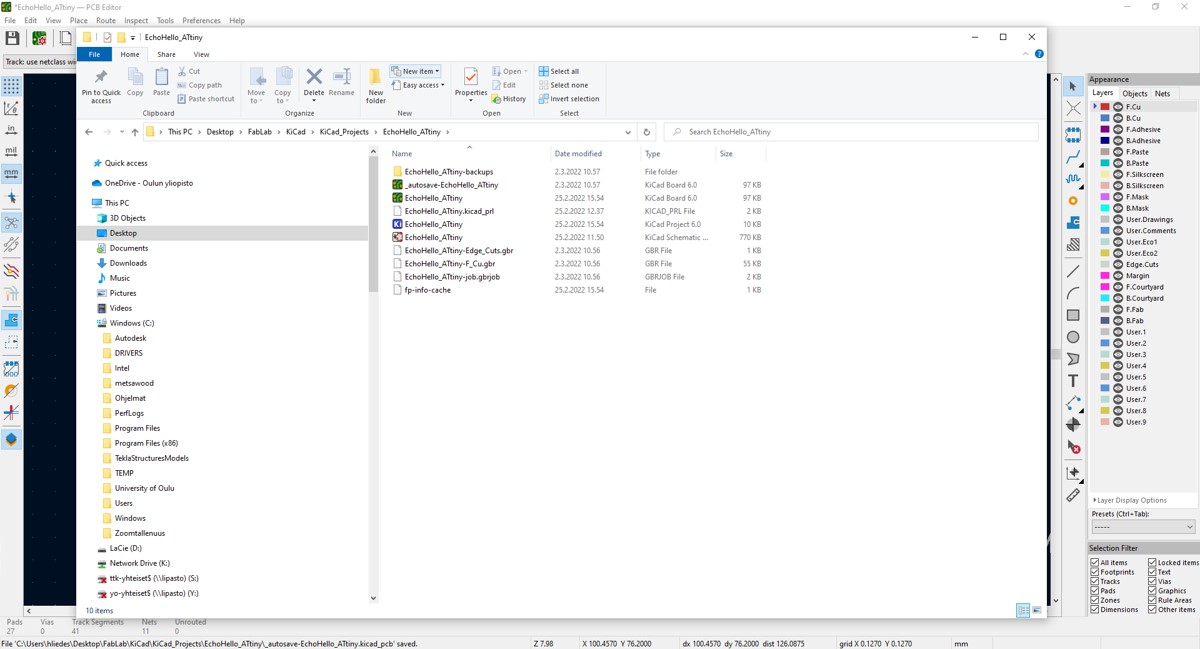
Files
KiCad files
.SCH EchoHello_ATtiny.kicad_sch
.PCB EchoHello_ATtiny.kicad_pcb
.PRO EchoHello_ATtiny.kicad_pro
Gerber format
.GRB EchoHello_ATtiny-F_Cu.gbr
.GRB EchoHello_ATtiny-Edge_Cuts.gbr
SVG format