5. Electronics production
Group assignment
- characterize the design rules for your PCB production process
The members of the group: * Achille Achille’s site * Anssi Anssi’s site * Jari Jari’s site * Hannu
Individual assignment
make an in-circuit programmer by milling and stuffing the PCB, test it, then optionally try other PCB processes
Group assignment
The principle of electronic circuit by shortly
An electronic circuit consists of different electronic components such as
resistors, diodes, ICs (integrated circuit) etc. Electronic components connected
by conductive wires or traces through which electric current can flow.
Traces role is to combine individual pieces of electronic components together into a single electronic circuit on a printed circuit board (PCB).
A printed circuit board (PCB)
PCB consist of non-conductive base material layer and conductive layer or layers. These different layers are laminated together. Usually base material is fiberglass and conductive layers are copper.
To make connections between different components on PCB it is necessary to remove part of copper layer. These connections on copper layer is called traces.
There are many different PCB manufacturing techniques. In Fab Lab Oulu we use milling to make traces on PCB.
PCB manufacturing
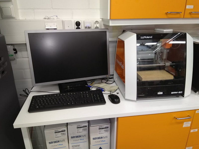
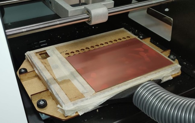
In Fab Lab Oulu main milling machine is Roland SRM 20 (see picture 1).
Testing
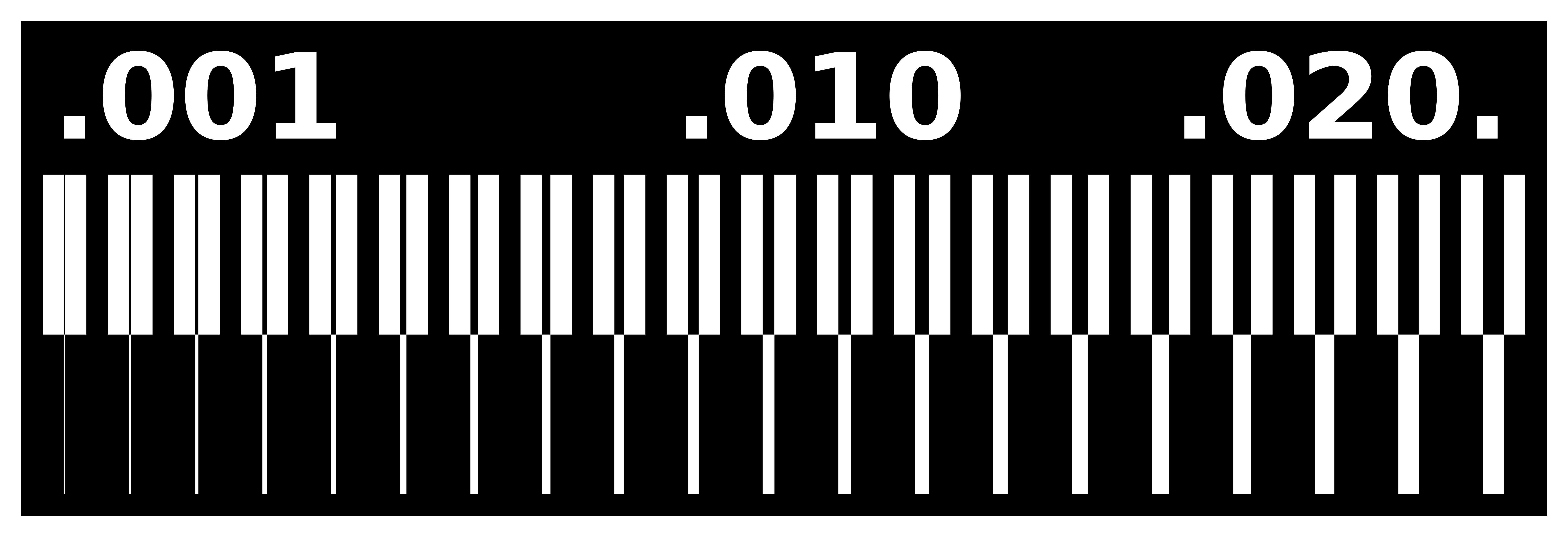
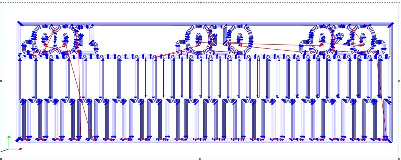
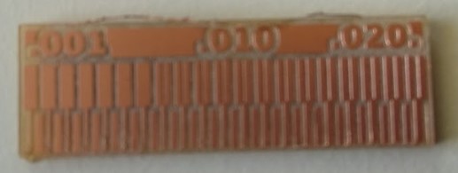
Before milling, we tested what is accuracy of milling process. Our local instructor Antti Antti Mäntyjärvi gave us files linetest.png and linetest.interior.png to testing.
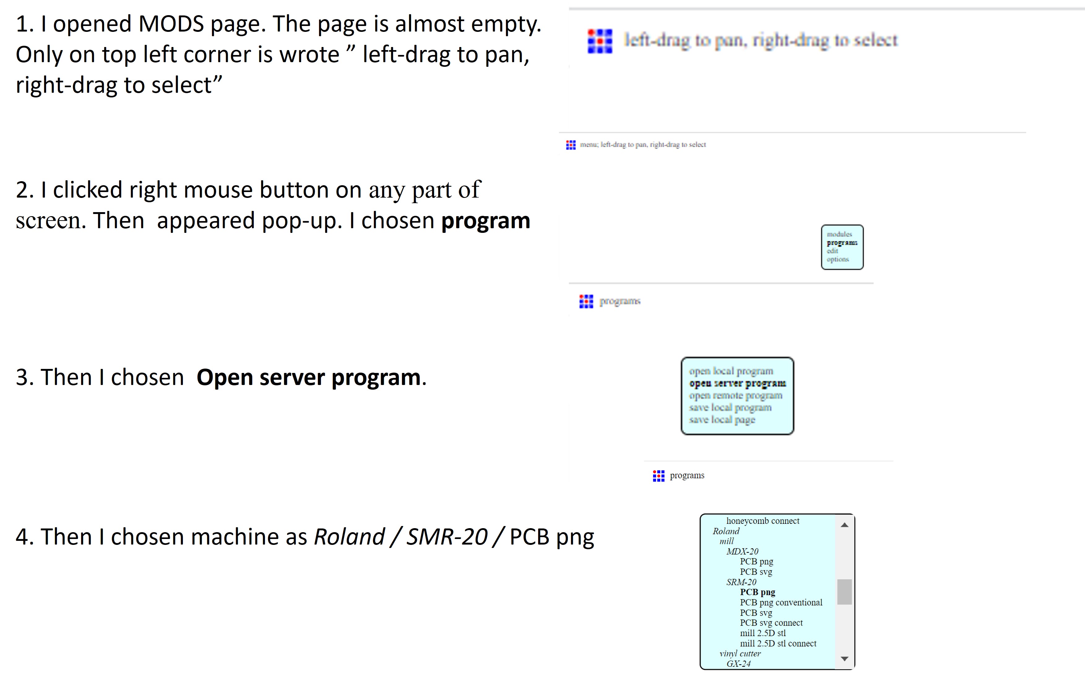
We went to http://mods.cba.mit.edu/. First we had to open the rights modules
Step 1. We open Mod and clicked Mouse Right-Click button on empty windos.
Step 2. We chose Programs
Step 3. Then We chose open server program
Step 4. And finally We chose Roland / SRM-20 / PCB png.
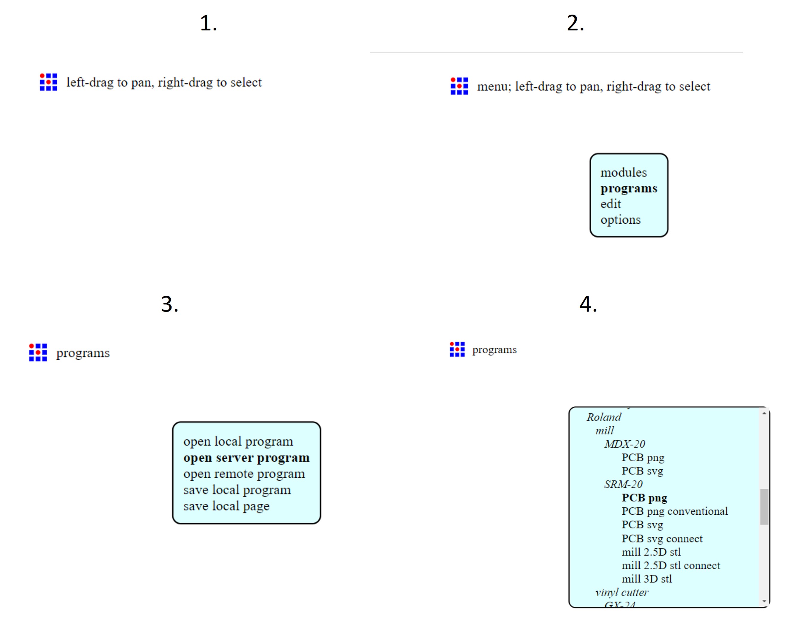
After steps 1-4. The Mods modules popped up on the window.
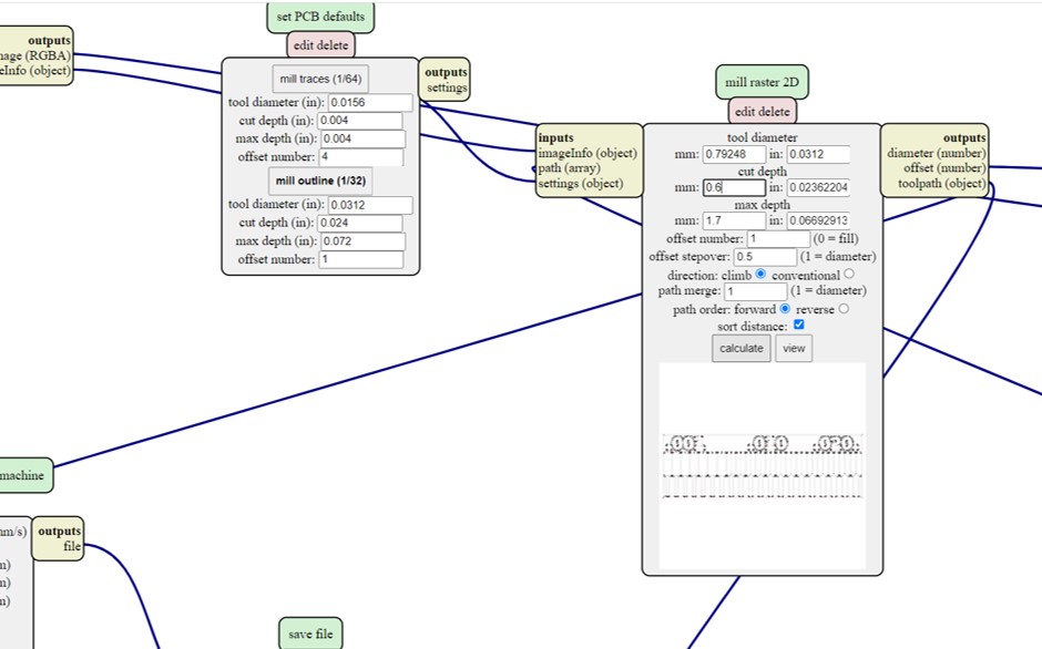
We setted next values to Mods modules to line test * Tool diameter 0.2 mm * Origo x:0, y:0 z:0 to origo
Step 1. We selected file linetest.png by clicking select png file. Step 2. We clicked mill traces Step 3. We setted tool diameter 0.0 mm Step 4. We setted values x:0, y:0 z:0 to origo. Step 5. At the end, we clicked Calculate button.
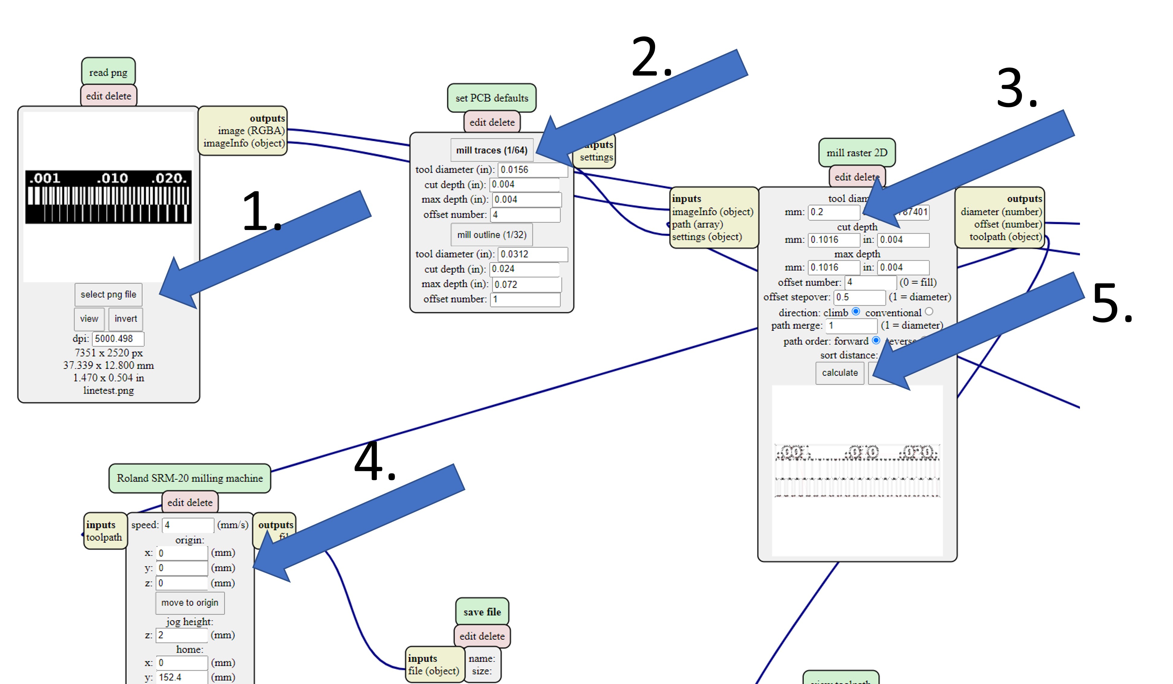
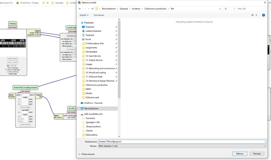
Then we saved file to PC
The next we made cutting path to remove our board at the same way. We used
- Cut depth 0.6 mm
- Max depth 0.6 mm
Milling
I tested Vacuum Table. It works very fine. I have documented milling process in Individual assignments.
At the finally we got test board
Individual assignments
- make an in-circuit programmer by milling and stuffing the PCB,
- test in-circuit programmer,
- then optionally try other PCB processes
Research
There are many ways to connect electrical components together by making electronic circuit. The oldest fabricate method is point-to-point construction. After that widely used technology was through-hole technology. Nowadays widely used technology is surface mount technology (SMT). This is method in which the electrical components are mounted directly onto the surface of a printed circuit board (PCB). https://en.wikipedia.org/wiki/Surface-mount_technology
In-circuit programmer (ICSP programmer) is device for In-Circuit Serial Programming (ICSP). ICSP based on In-System Programming (ISP) technique. ISP is a technique where a programmable logic devices (PLD) is programmed after the device is placed in a circuit board. https://en.wikipedia.org/wiki/In-system_programming
A programmable logic device (PLD) is an electronic component used to build reconfigurable digital circuits. https://en.wikipedia.org/wiki/Programmable_logic_device
Shortly our assignment was fabricate UPDI programmer by using surface mount technology (SMT) . This means that PCB fabricated without holes for components (vs. Through-hole technology). We made traces to connections by milling technique. In Oulu we use Rolland SRM20 mill.
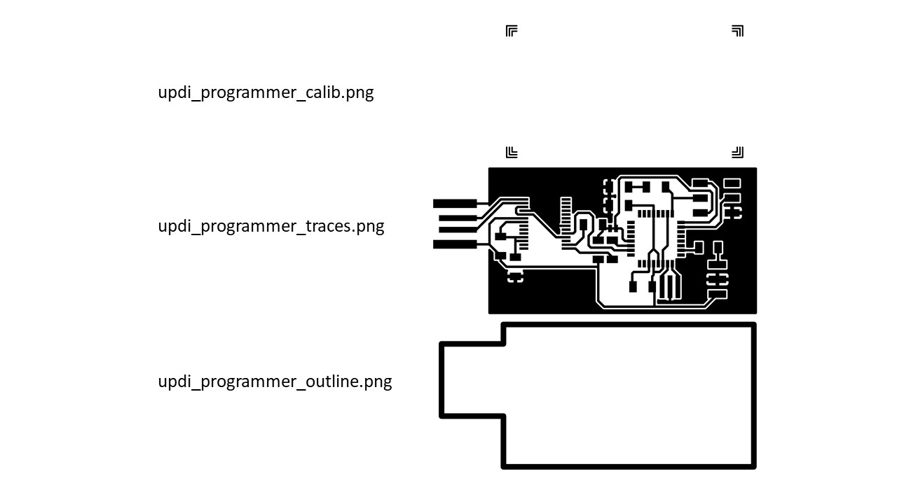
In this assignment we can use ready-made toolpath files (.png files) for traces, calibrations and outlines. Github https://github.com/fablaboulu/updi_arduino_programmer
Plan to work flow
- Create tool paths files (.rml files) for milling
- Milling the PCB
- Stuffing the PCB
- Programing
- Test programmer
PCB
First I downloaded .png files from Github. Then I created milling files (.rml files) using MIT Mods-system.
MIT MODS
Mods is a browser-based environment for data handling, toolpath planning, and machine execution. http://mods.cba.mit.edu/
Next steps 1 - 4 are similar all file creating.
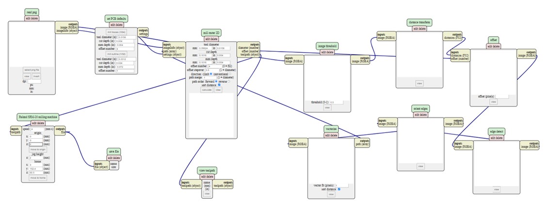
at last I got Mods modules
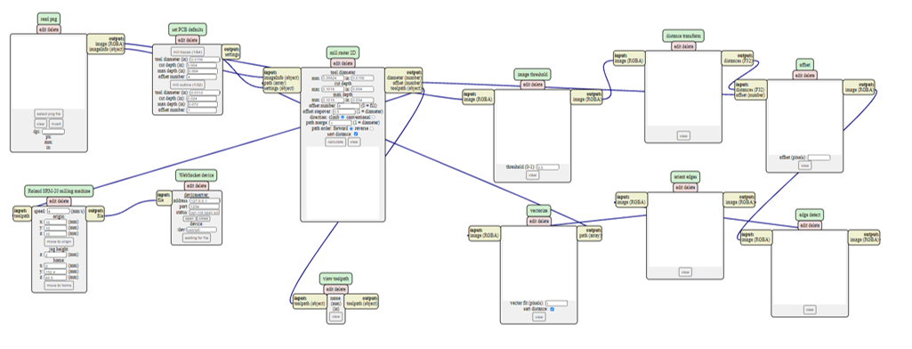
Before I started create files I had to know PCB material I will use.
A. Create Calibration file
Step 1. I clicked select png file button
Step 2. Then chosen pop-up menu updi_programmer_calib.png file from my PC-
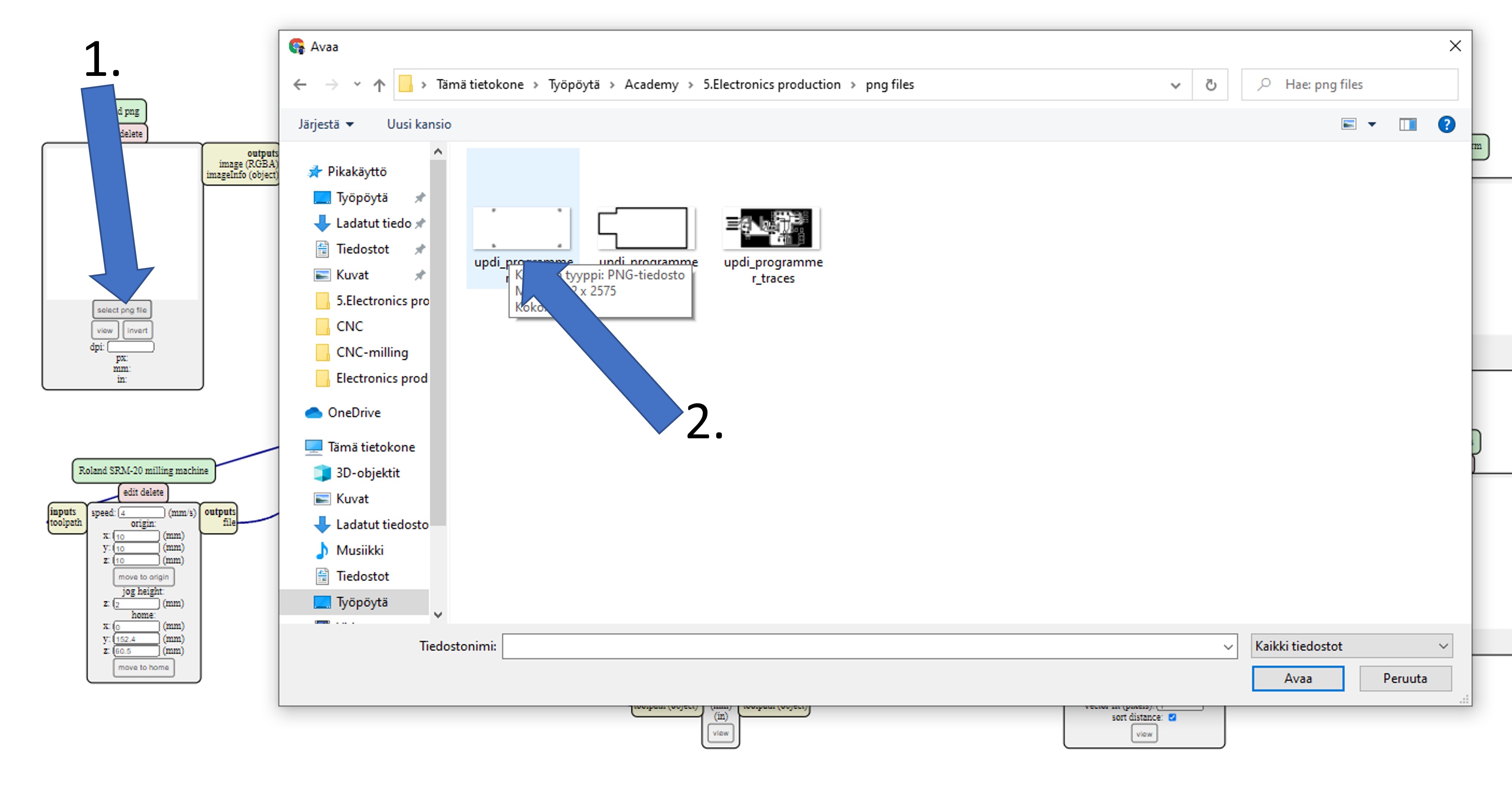
Step 3. When file was uploaded, png picture appeared to read png module.
Step 4. In this menu I setted mill traces to 1/64
Step 5. In this menu I typed next data
- tool diameter to 0.23mm.
- cut depth to. 0.1mm.
- offset number to 5.
- offset stepover to 0.5.
Step 6. In this menu I setted origin (x0, y0, z0) to zero.
Step 7. Then I had to deleted Websocket device.
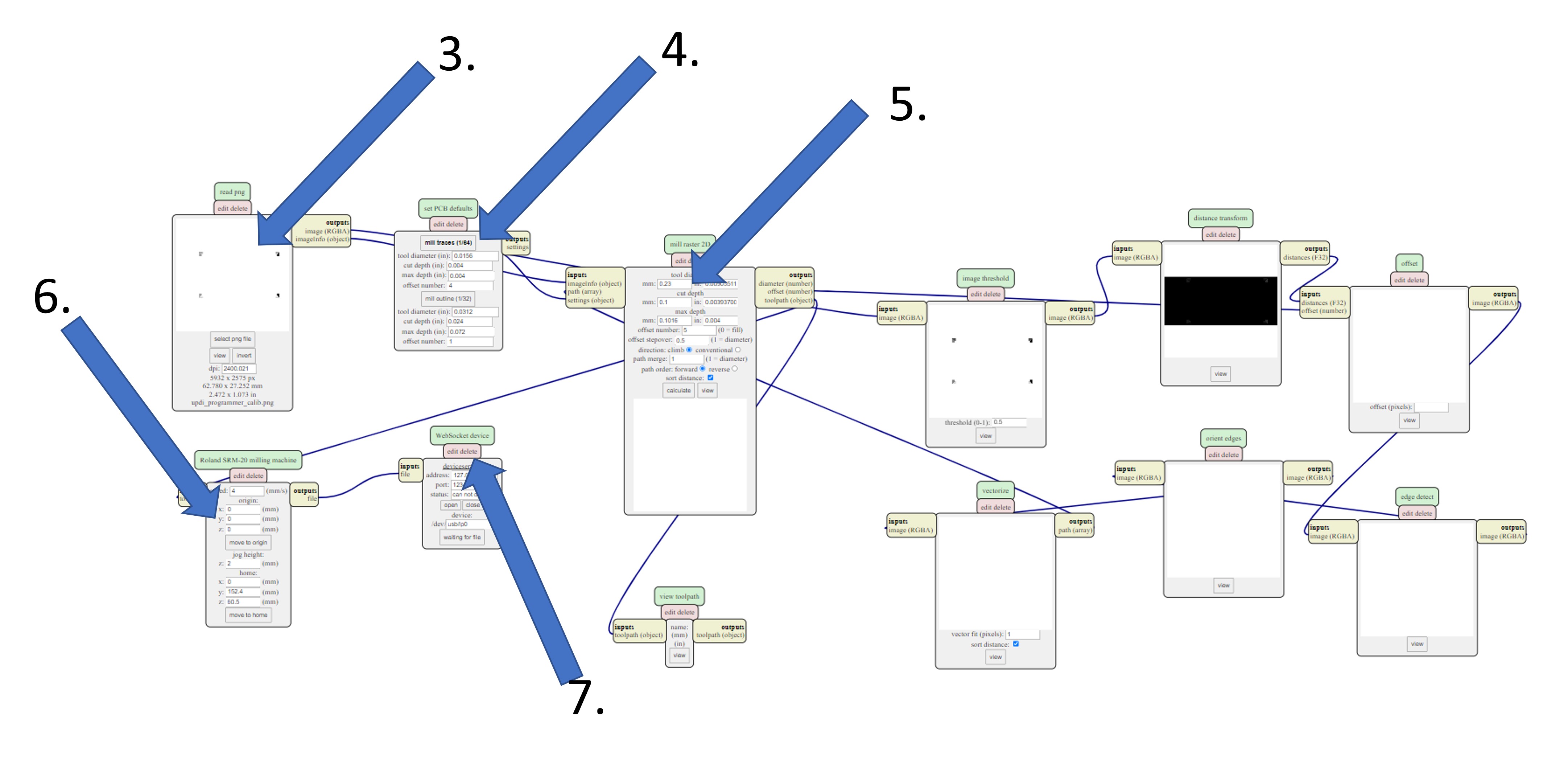
Step 8. After deleting Websocket device was disappeared.
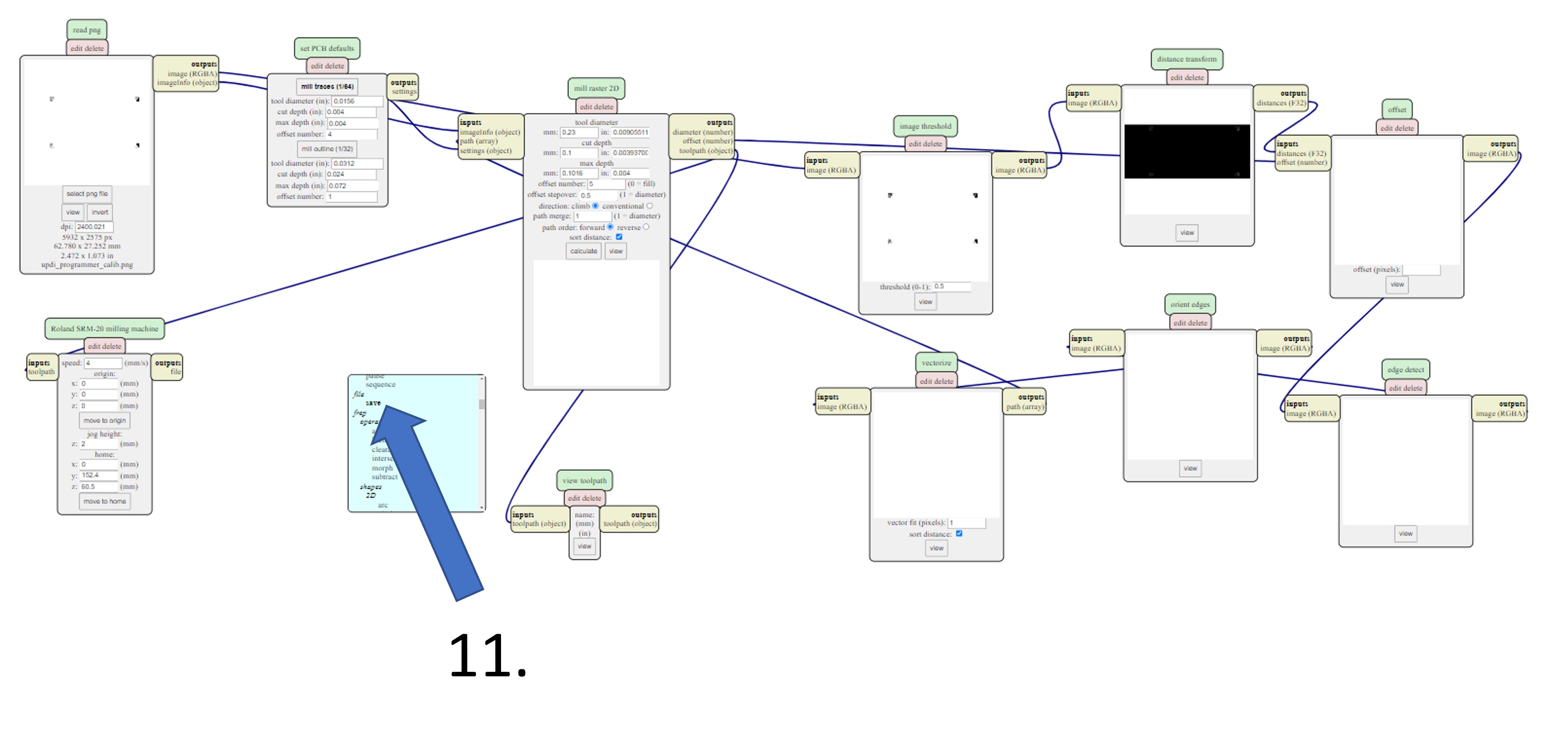
Step 9. Then I added new file safe module. First I clicked right mouse button on screen and then modules on popup list.
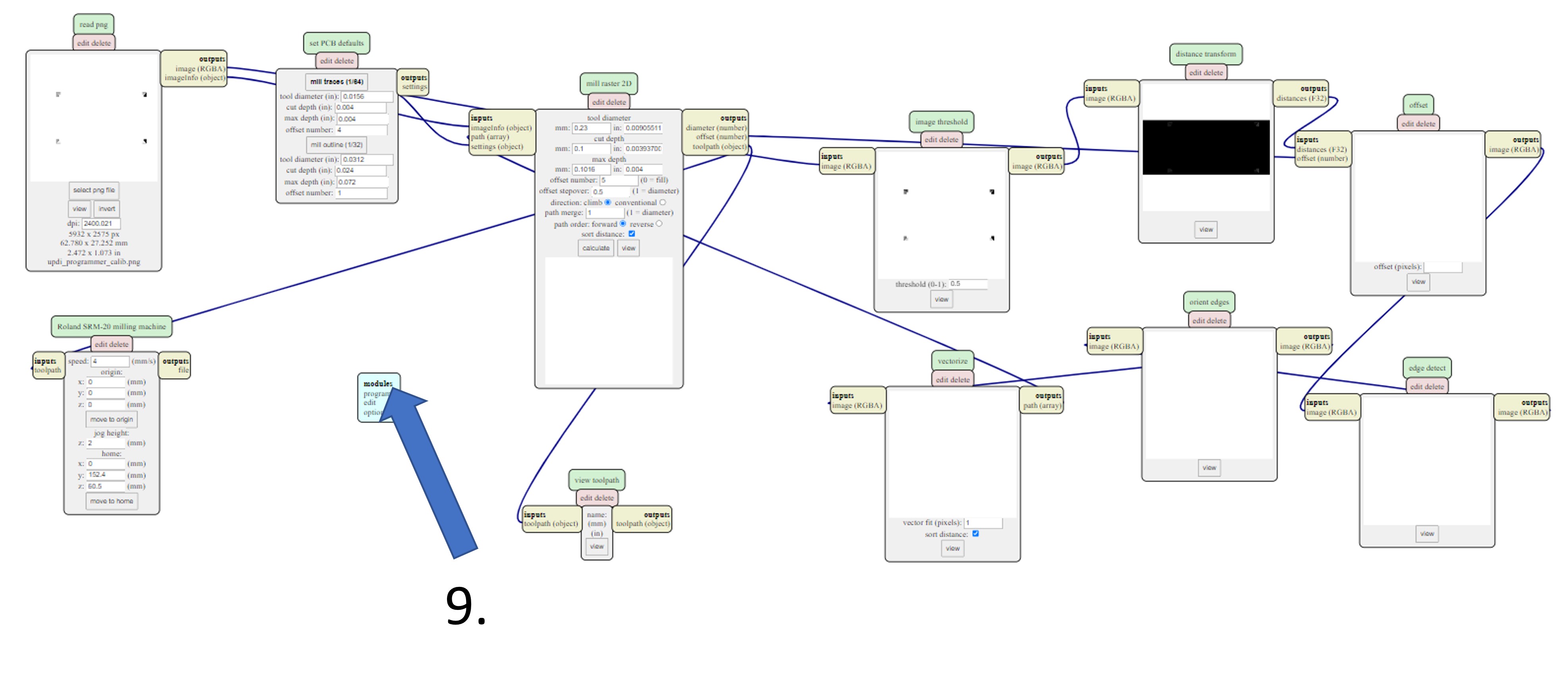
Step 10. Then I clicked open serve module.

Step 11. Then I clicked file/save.
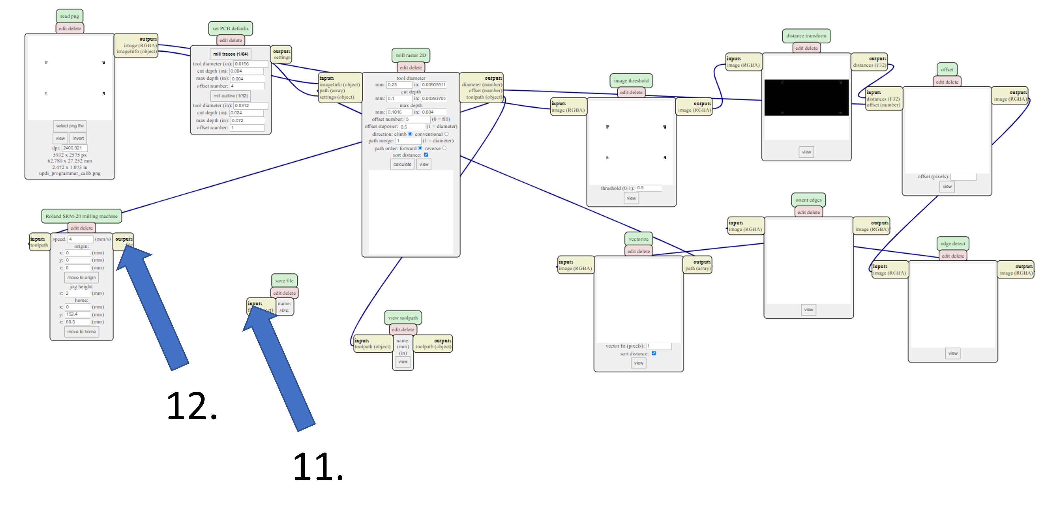
Step 11. To make connection I clicked first file on Rolad SRM-20 milling machine module
Step 12. And then clicked file (object) on save file module
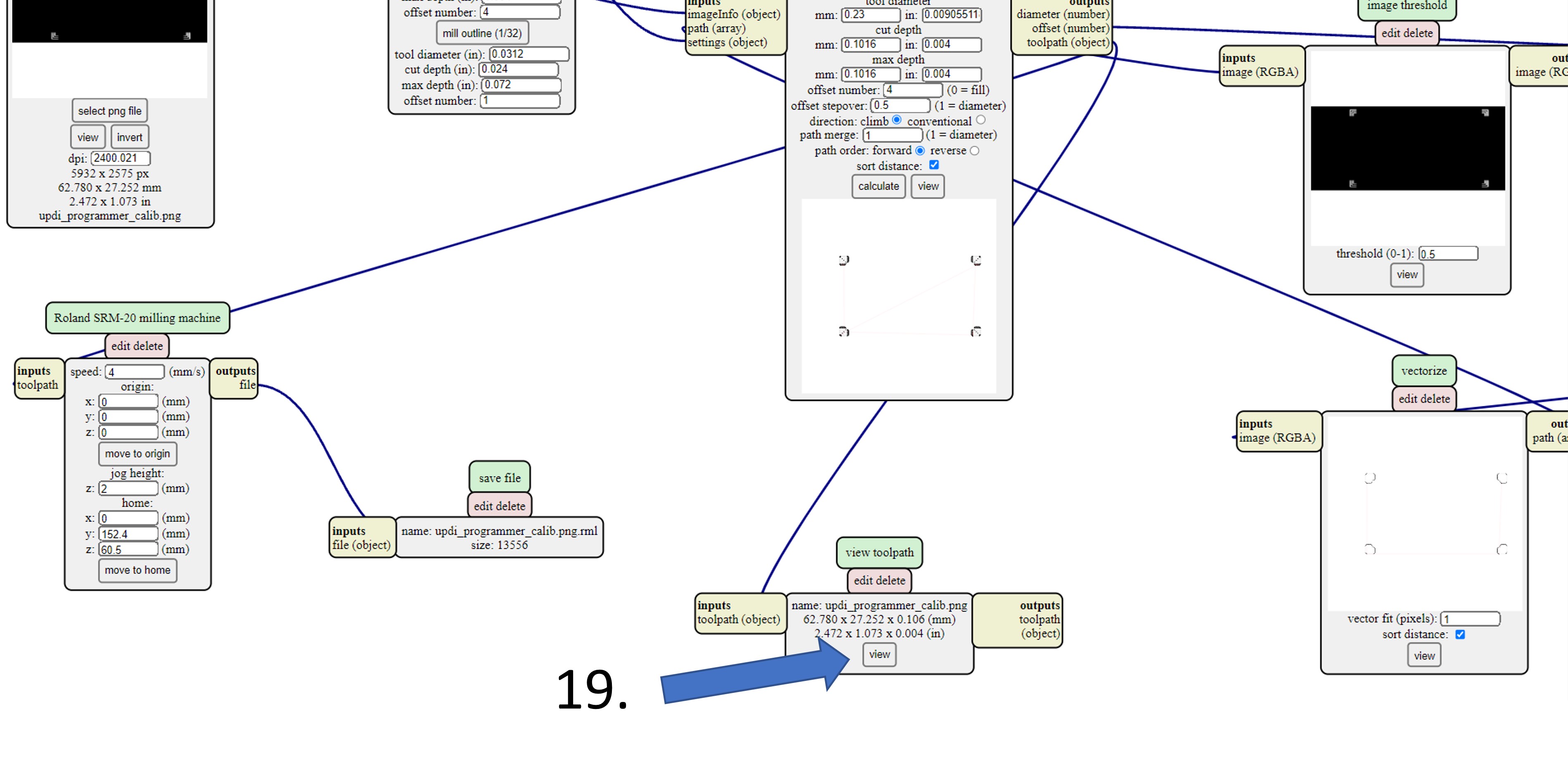
Step 13. I clicked Calculating button on Mill raster 2D module. Then popped up save file window. I safed file updi_programmer_calib.png.rml to my PC
Step 14. To view toolpath I clicked view button on view toolpath module
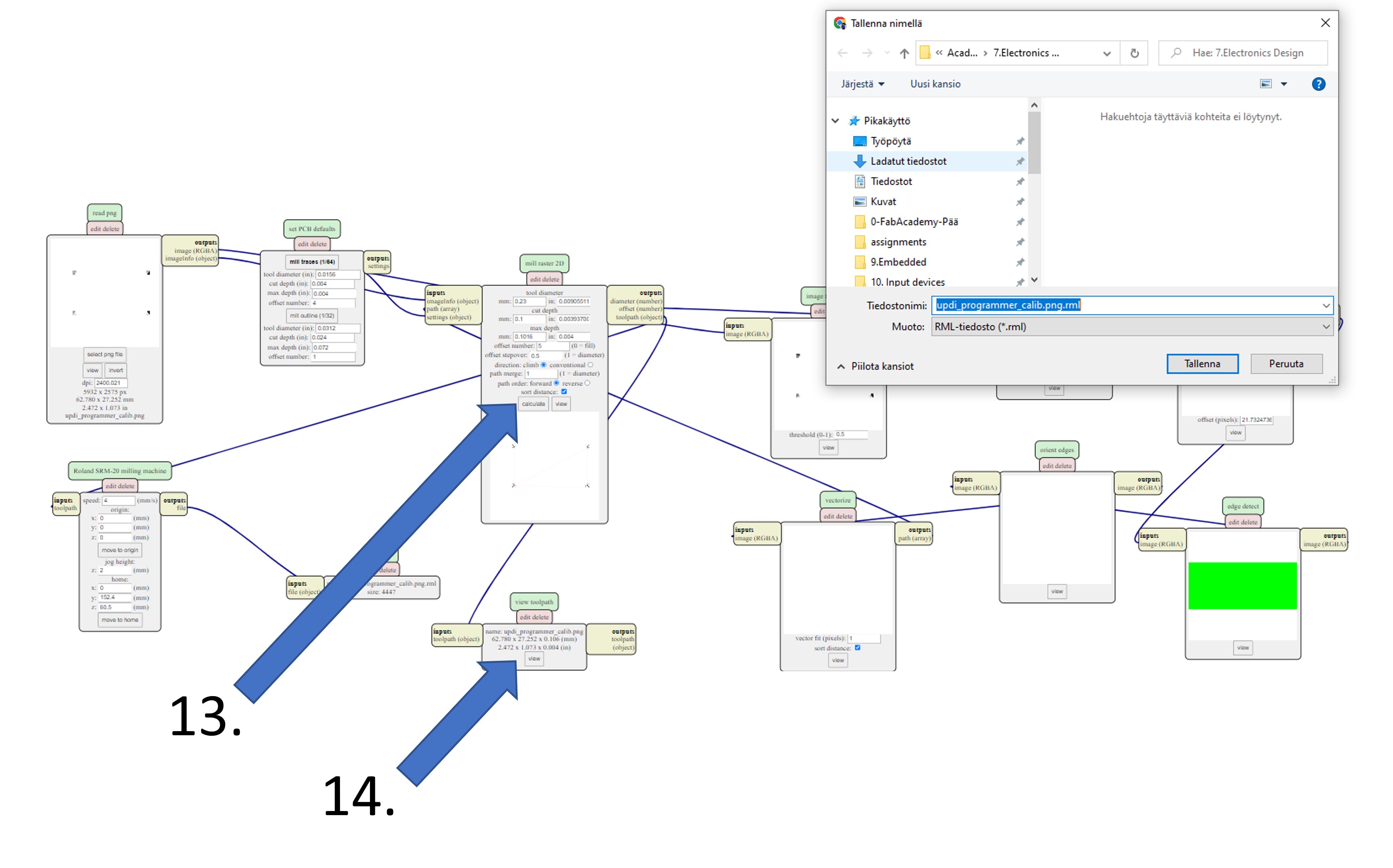
Step 15. At last created toolpaths were ready to view on popup window.
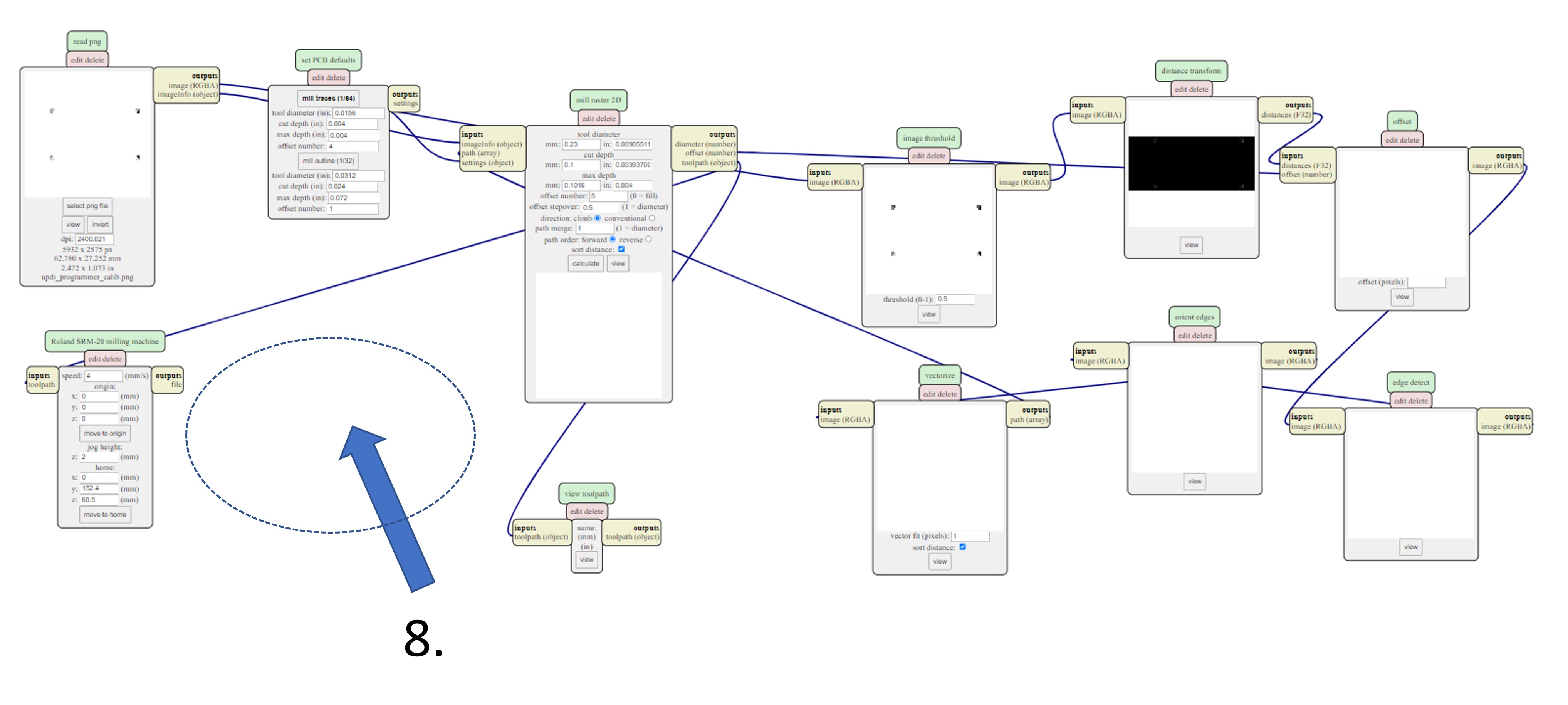
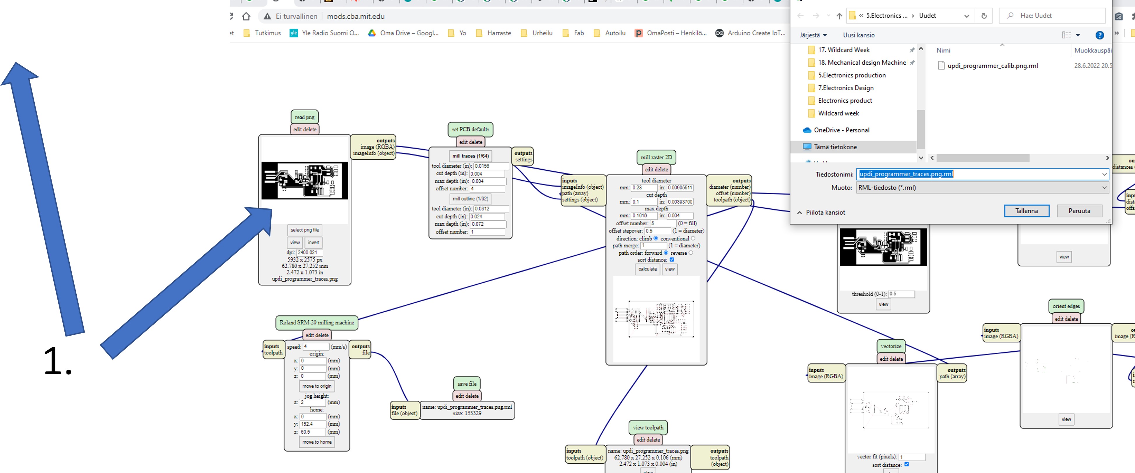
B. Create Traces file
Step 1. I created traces toolpaths same way as Calibration toolpaths but I had to invert traces file updi_programmer_traces.png in Read png module
C. Create Outlines file
At last I created traces Outlines file same way as Calibration andTraces toolpaths but Tool diameter in mill raster 2D module is 1mm (flat) and Cut depth is 0,6 mm.
Milling
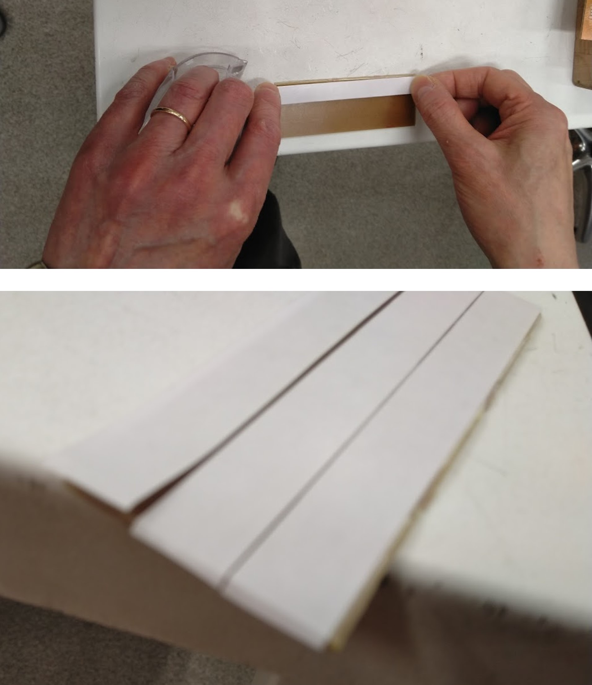
First I cut fitting size from FR-1-PCB blank to PCB.
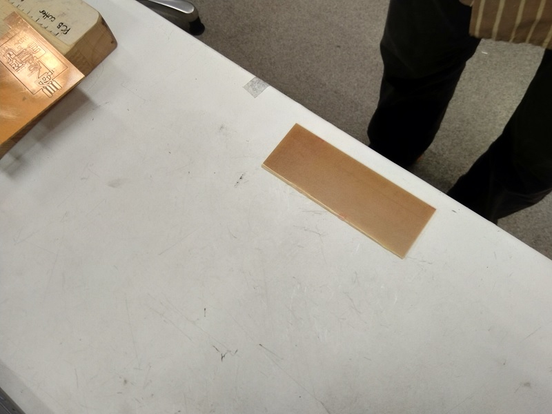
I used double sided tape to set cut piece tight on the milling machine.
It is very important to mount PCB very tight onto the Work plate. So I cleaned Work plate using a vacuum cleaner. Then I pushed PCB very hard onto Work plate.
I mounted the milling bit to the Spinder motor. First I released spindler collect using a hex key then I setted bit with between two fingers to the Collect and the rest I tightened the Collect using a hex key.
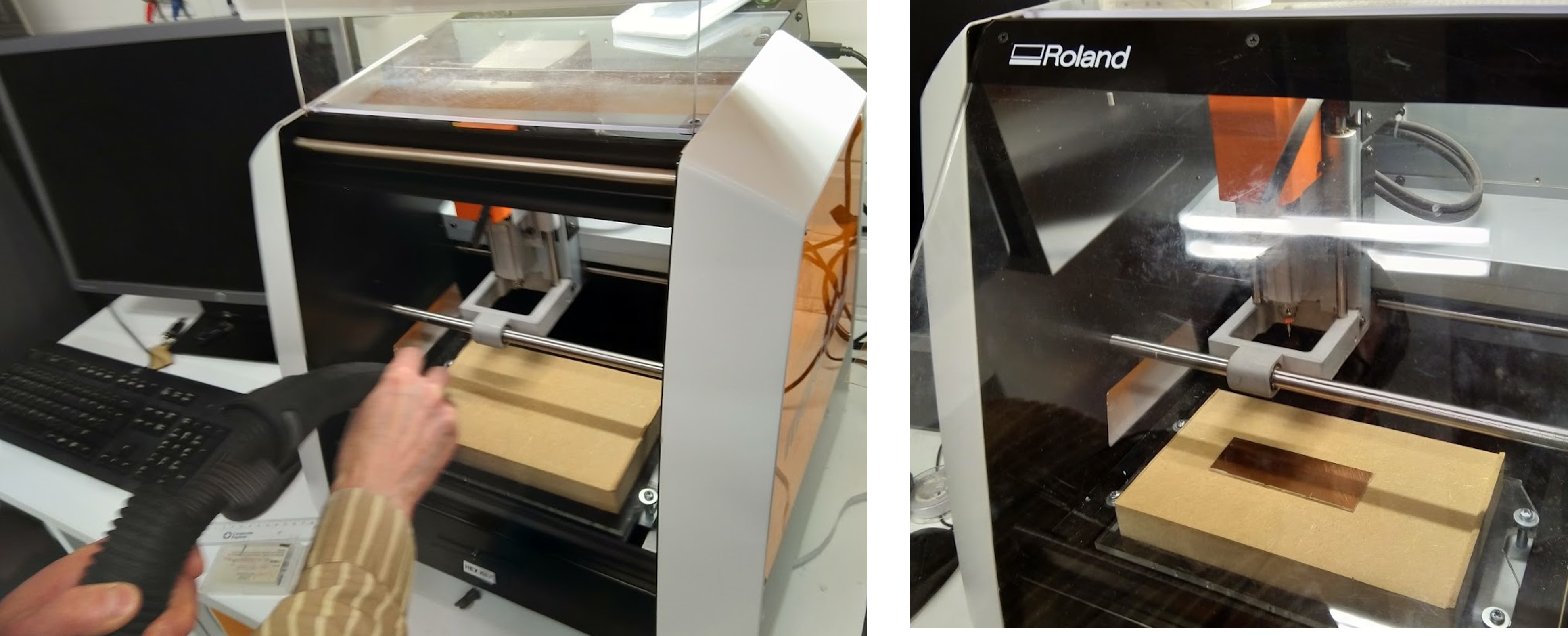
I opened VPanel to mill PCB.
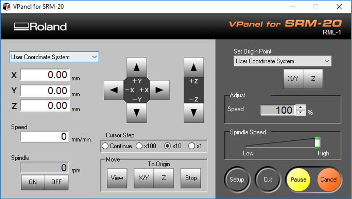
First I orient bit to the lower left corner on PCB
I moved bit using on horizontal level using -x,+x, -y and +y buttons (B) and rest I setted it to by push button x/y (D). On vertical leve I used -z and +z buttons. I moved bit very near the surface of the PCB. Then I released the Spinder Collect using a hex key but holding bit at the same time two fingers and set bit onto the surface of the PCB. Then I set Z-level by push button z (D). After settings coordinates x, y and z were zero (A).
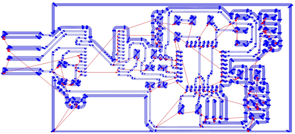
After orientation of bit I loaded toolpath files by push button Cut (E) and menu Cut popped up (Sorry blurry picture).
First I clean Output File List by pushing button Delete All. Then I loaded updi_programmer_calib.png.rm file to mill calibration paths. I started milling by pushing button Output.
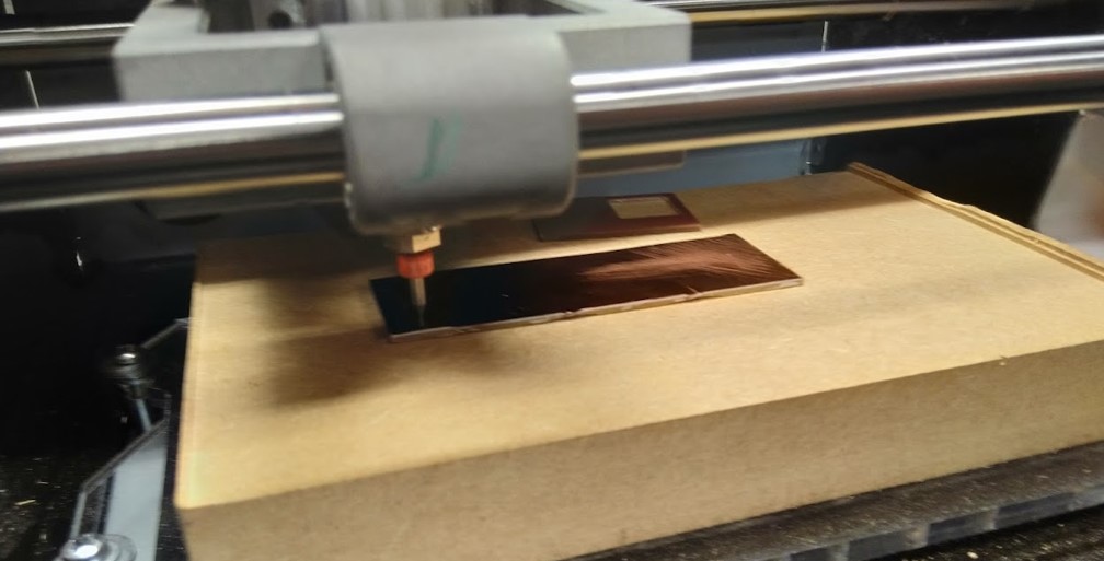
After calibration paths milling I checked milled paths. Then I milled same way Traces and Outlines.
When PCB was milled I cleaned it using steel wool.
Stuffing
I got componet list from Eagle file. I collected Components from the componet stock of Oulu Fab Lab.
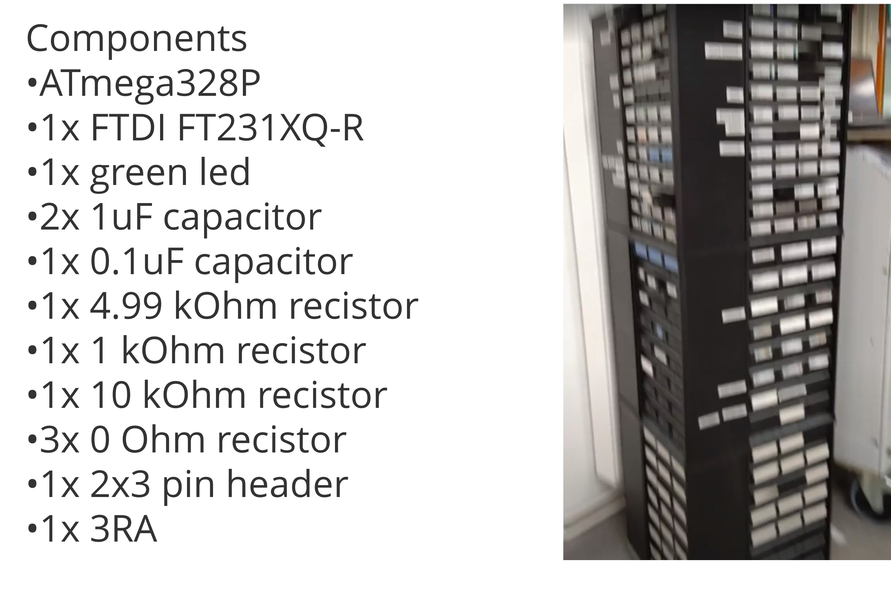
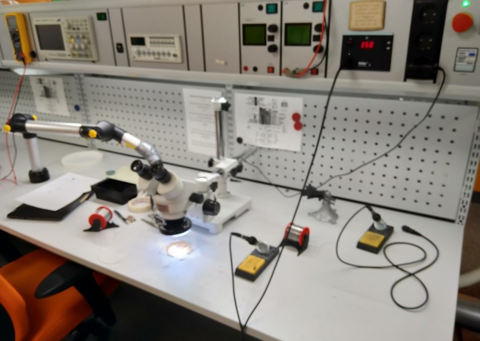
I soldered componets on the electronic workstation of Oulu Fab Lab.
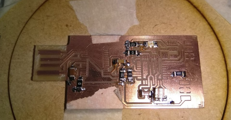
During soldering work the connector was detached. The detached connector remove also pads.
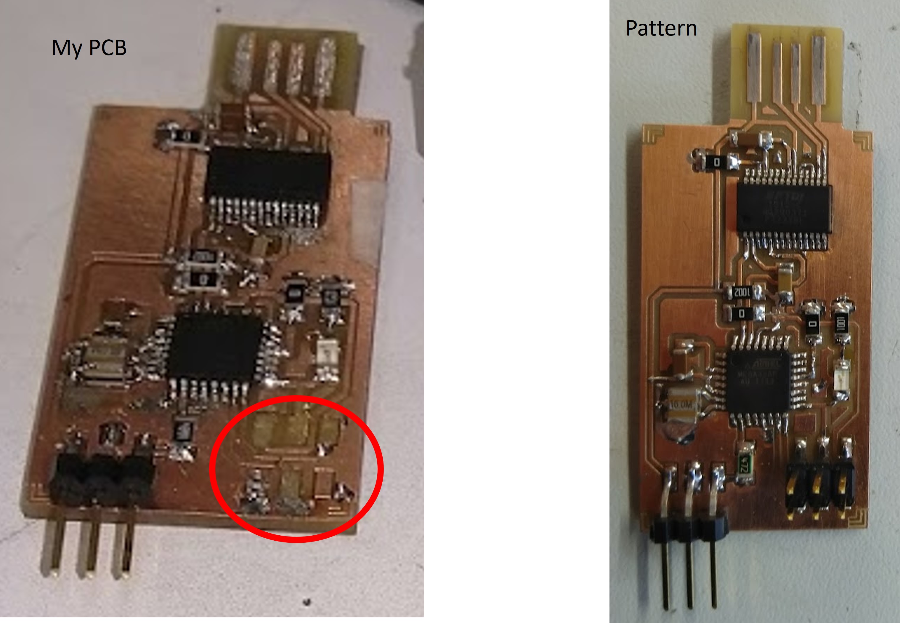
Our local istructor Antti Mäntyjärvi help me to solve problem. He guided to solder narrow wires to losen pads.
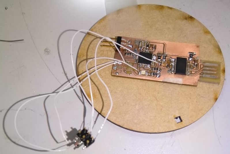
After soldering I checked board with a multimeter to avoid possible short circuits. The board was ok. So, next step was to program new board to programmer.
Programming the programmer and tests
To program my new upcoming programmer I needed ready-made programmer. Local istructor Antti Mäntyjärvi gave me that one. Then I conneted my new programmer to ready-made programmer and then it to my laptop’s USB port.
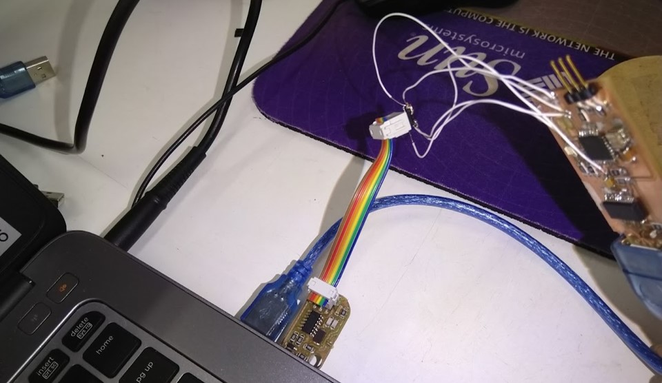
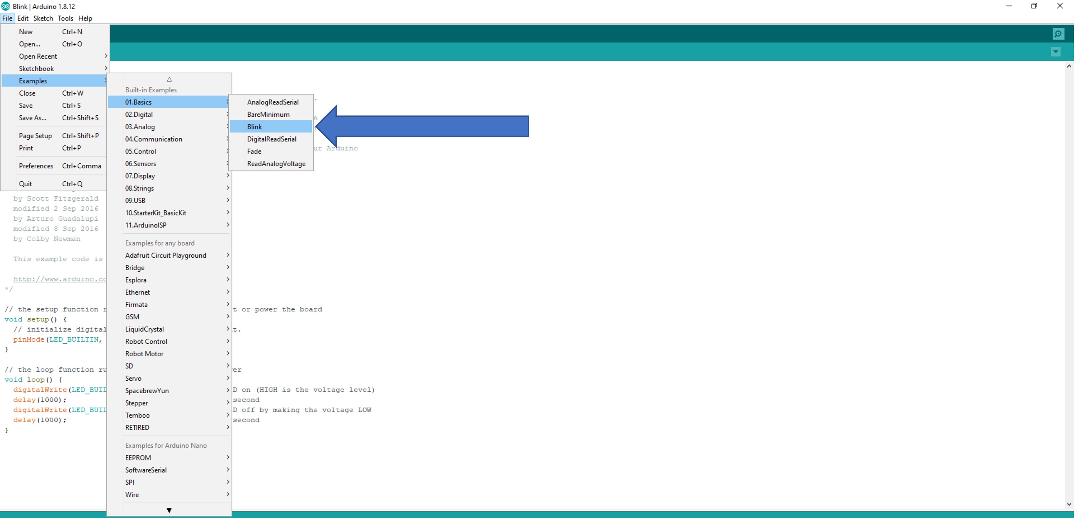
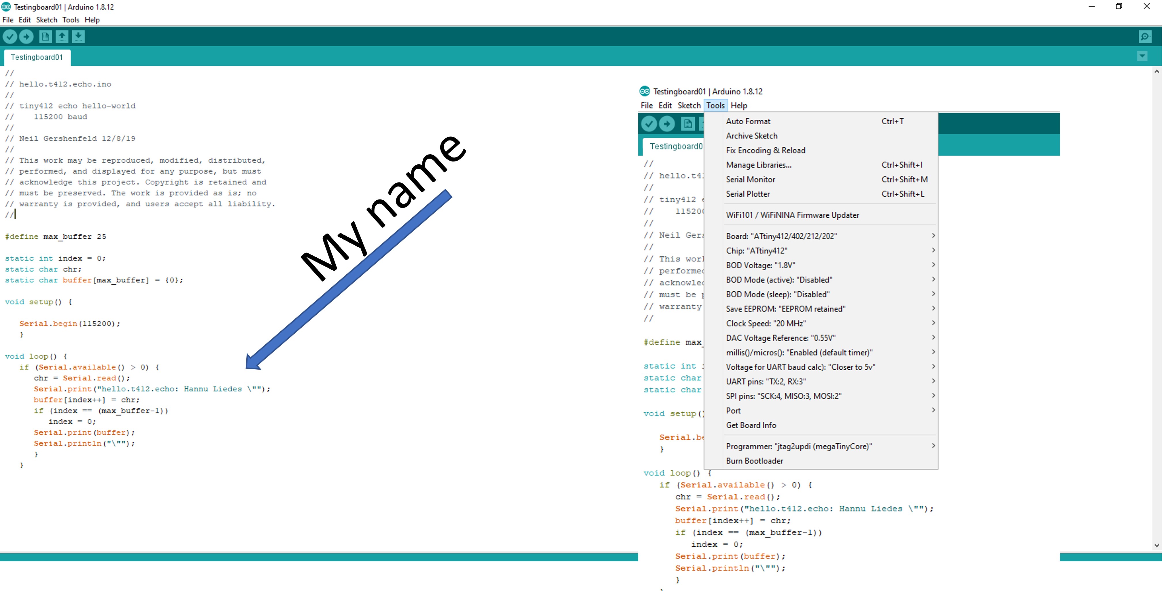
Then I open Arduino Software (IDE) to test my new upcoming programmer. I open the Tools-menu in Arduino Software (IDE) and I loaded very simple Blinking code.
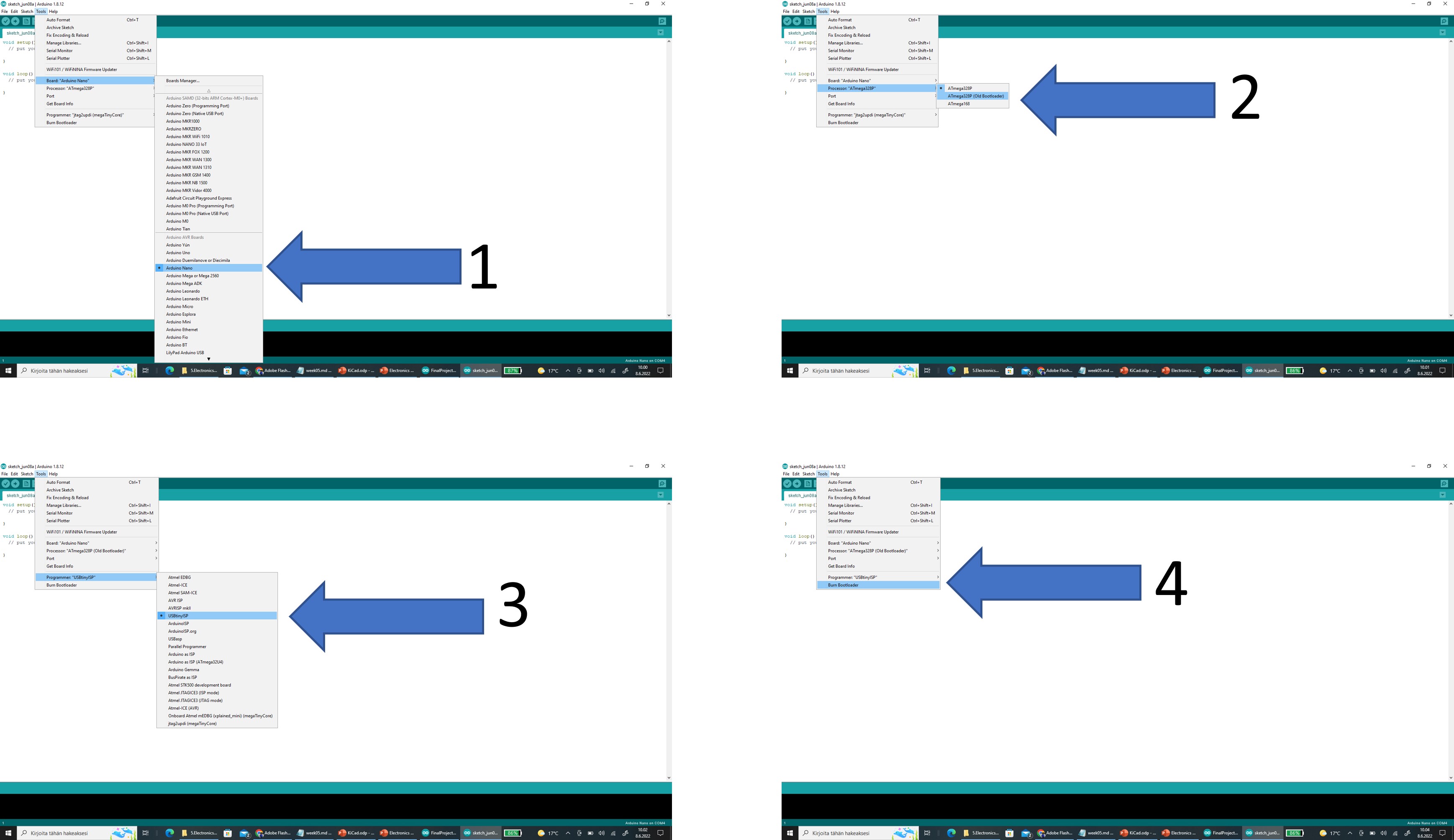
Then set next values in Arduino Software (IDE) : - Board: Arduino Nano (1) - Processor: ATmega328P (Old Bootloader) (2) - Port: COM5 (Port, in which programmer is connected. I checked it from device manager) - Programmer: USBtinyISP (3) - Press Burn Bootloader (4)
After that led should be blinking and working as Arduino -board, but in my bord that is not happend. I discussed that problem with instuctors. They belived that led was oriented backwards. So, I continue programming process.
UPDI programmer
First I downloaded jtag2updi from github. Then I unpacked it. Note that all the files should be in the same directory with jtag2updi.ino sketch file.
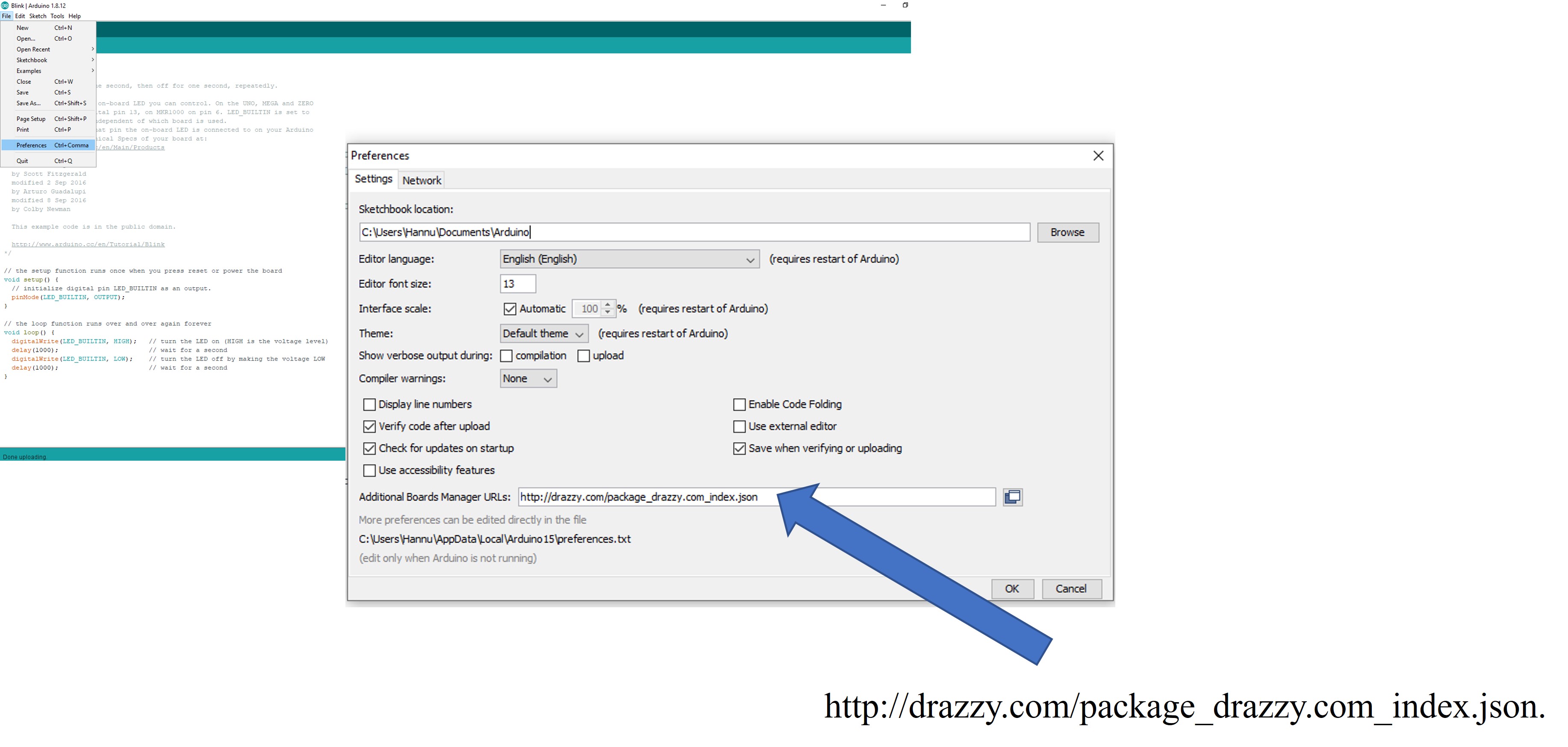
After that I opened the Preferences Popmenu. I typed URL adderess http://drazzy.com/package_drazzy.com_index.json to Additional Board Manager URLs.
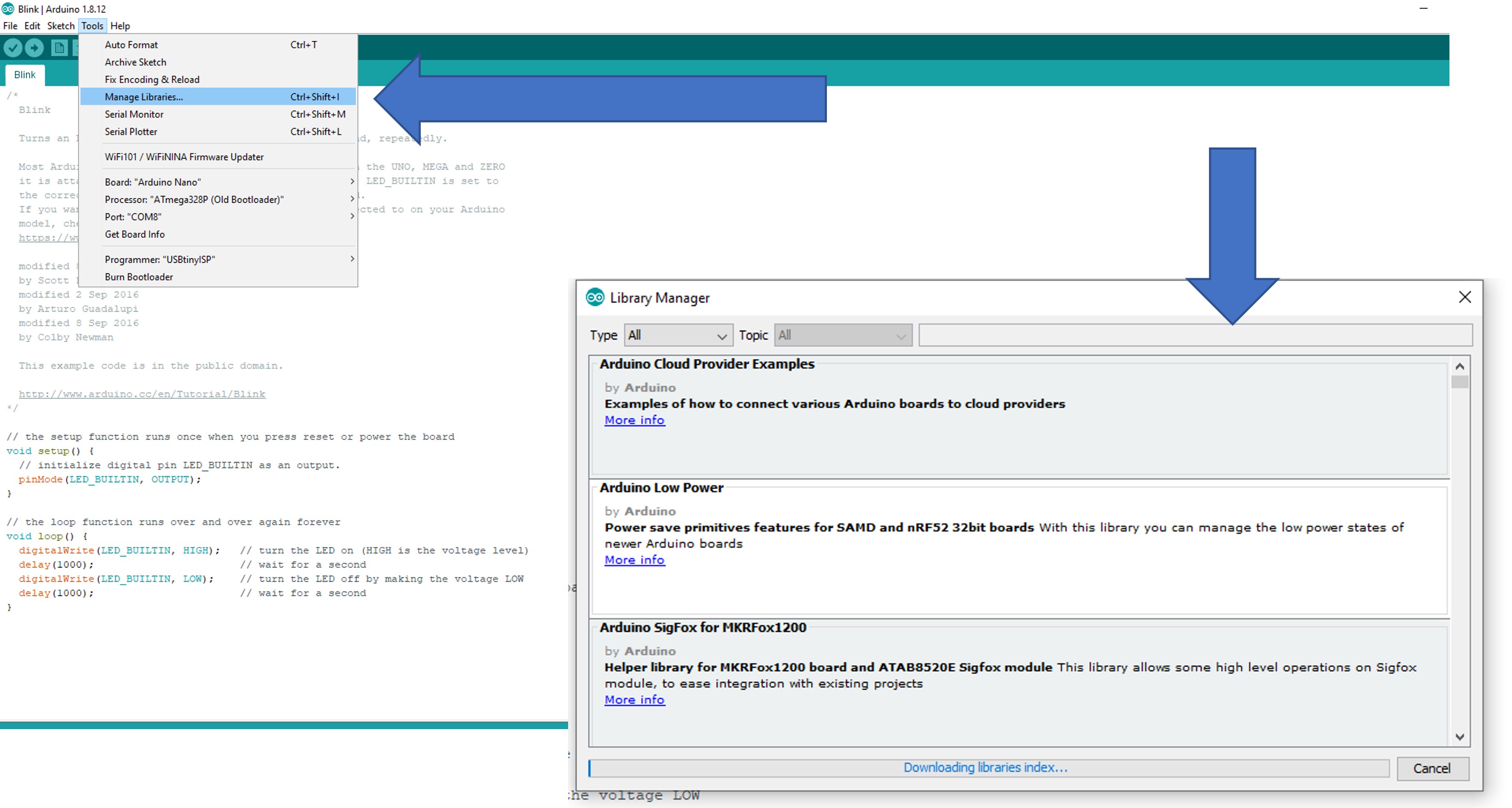
Next I downloaded megaTinyCore and megaAVR Boards to Arduino Software (IDE) one by one Manager Libraries…
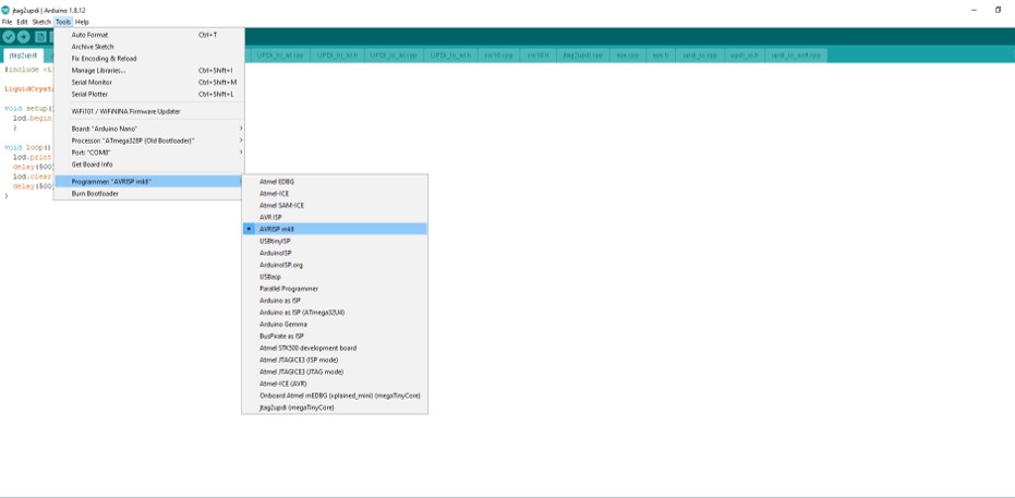
Then open the jtag2updi.ino and set next values - Board: Arduino Nano - Processor: ATmega328P (Old Bootloader) - Port: COM5 (or which ever yours is attached) - Programmer: AVRISP mkll
At last Press Verify and Upload
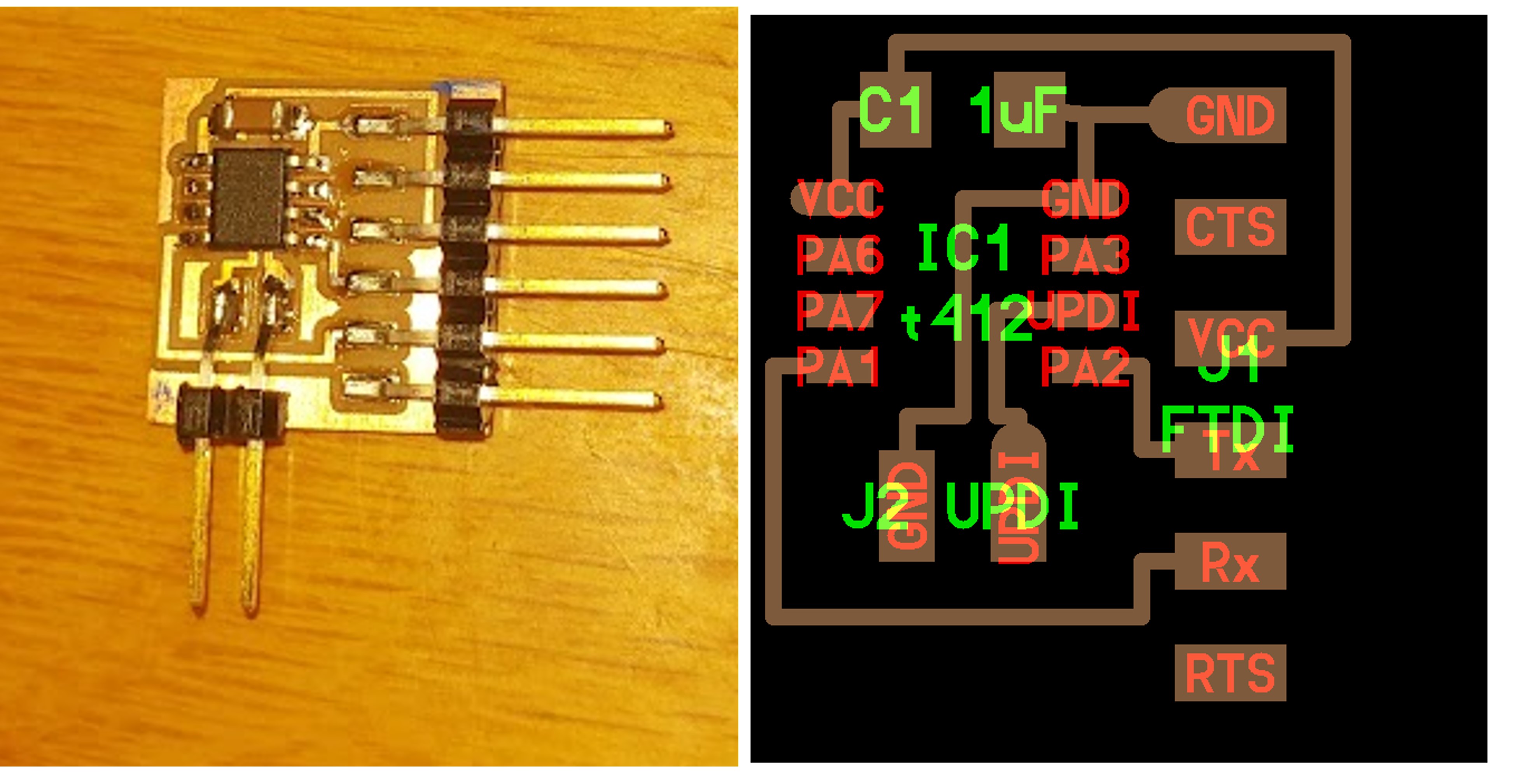
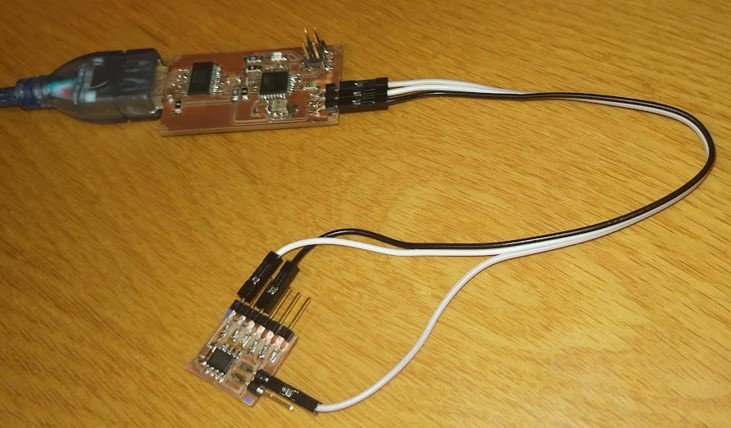
Then I cut path from microcontroller to FTDI. The next step is programm new upcoming programmer to UPDI programmer
Finally I got my own UPDI programmer.
Testing
Then I tested my new programmer by ready made test board (Neil’s echo board). I programmed it and then I checked was it successful.
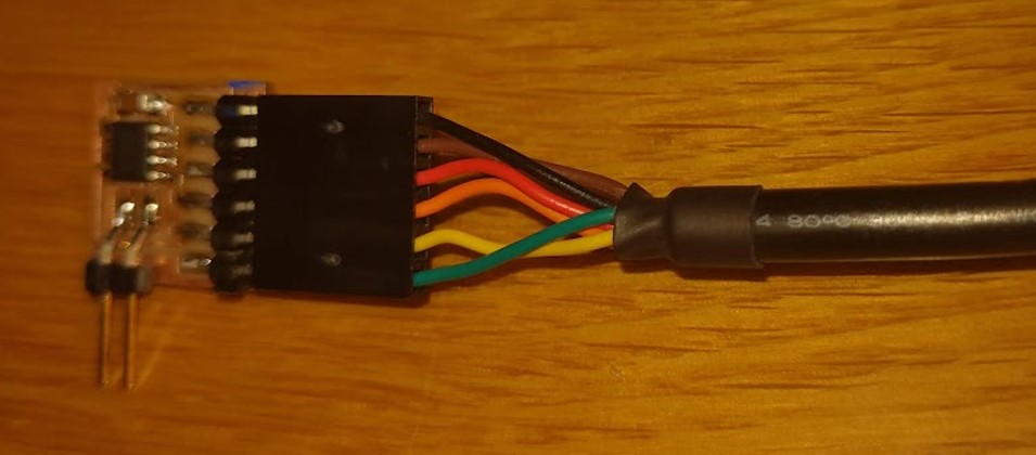
I connected echo board to my UPDI programmer by jumper wires (Gnd to Gnd, Vcc to Vcc and UPDI to UPDI)
After that I copied echo code from Fab Academy site (http://academy.cba.mit.edu/classes/embedded_programming/t412/hello.t412.echo.ino) and pasted to Arduino. I changed my name to text “hello.t412.echo: you typed "“. This code send message to serial port (COM).
http://academy.cba.mit.edu/classes/embedded_programming/t412/hello.t412.echo.png
//
// hello.t412.echo.ino
//
// tiny412 echo hello-world
//    115200 baud
//
// Neil Gershenfeld 12/8/19
//
// This work may be reproduced, modified, distributed,
// performed, and displayed for any purpose, but must
// acknowledge this project. Copyright is retained and
// must be preserved. The work is provided as is; no
// warranty is provided, and users accept all liability.
//

#define max_buffer 25

static int index = 0;
static char chr;
static char buffer[max_buffer] = {0};

void setup() {

   Serial.begin(115200);
   }

void loop() {
   if (Serial.available() > 0) {
      chr = Serial.read();
      Serial.print("hello.t412.echo: Hannu Liedes \"");
      buffer[index++] = chr;
      if (index == (max_buffer-1))
         index = 0;
      Serial.print(buffer);
      Serial.println("\"");
      }
   }
Then I pasted code Arduino and
put next values to Arduino - I open Arduino - Board: ATtiny412/… - Chip: ATtiny412 - Port: COM5 (or which ever yours is attached) - Programmer: jtag2updi
At last I Pressed Verify and Upload. After that echo board has got new code.
Then I removed programing connections and connected echo board to my PC with USB UART Cable.
After I was ready to check that echo board send messages to serial port. First I checked what is COM port to echo board in Device Manager. Then I opened PUTTY program and set next values - Connetino type: Serial - Serial line: COM 6 (in my case) - Speed: 115200 (Same in code)
Then I pushed Open button
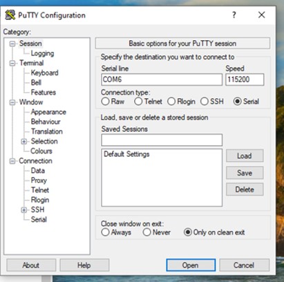
After that I Serial Port windows was opend. Then I pushed Enter button and I got “message hello.t412.echo: Hannu Liedes "
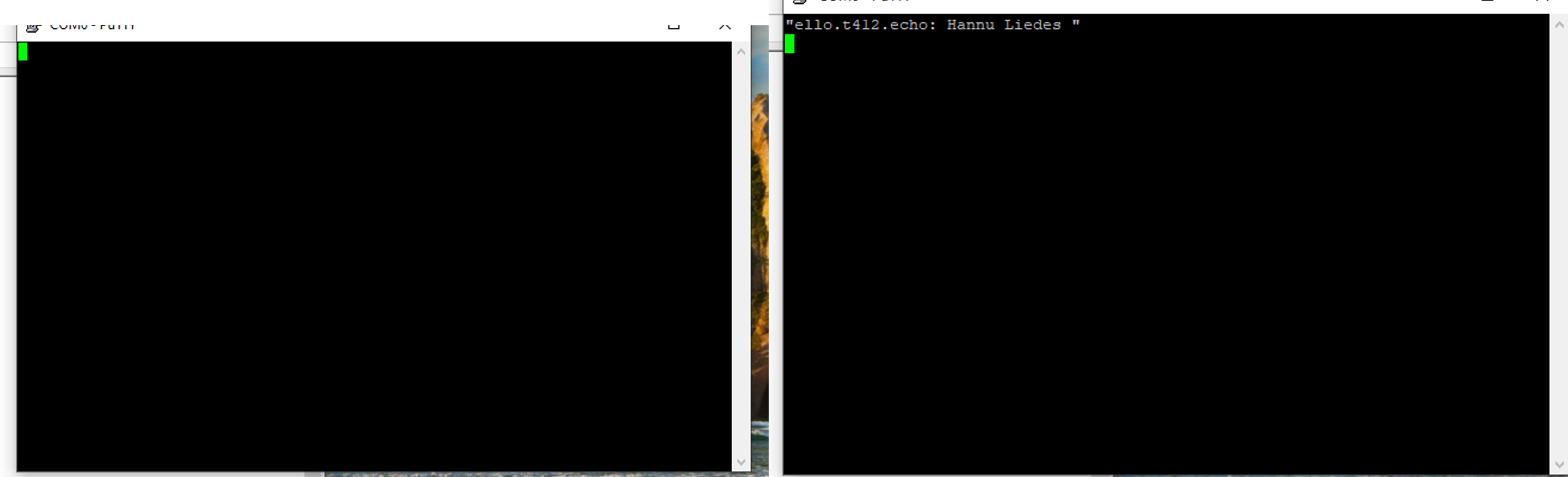
That was great. My programmer works very well.
Files
PNG files
.PNG updi_programmer_calib.png
.PNG updi_programmer_traces.png
.PNG updi_programmer_outline.png
RML files
.RML updi_programmer_calib.png.rml
.RML updi_programmer_traces.png.rml
.RML updi_programmer_outline.png.rml
Reflection
I learned lot of electronic such as PCB desing process, PCB fabricate process and embedding programming.
Tip to
It coud be good idea make a small Carrying Case for UPDI programmer by 3D printing (assignment on 3D Scanning and printing week).