| HOME | ABOUT ME | FABLAB UPM | FINAL PROJECT |
| week 1 Principles and practices, project management |
| week 2 Computer-aided design |
| week 3 Computer-controlled cutting |
| week 4 electronics production |
| week 5 3D scanning and printing |
| week 6 electronics design |
| week 7 computer-controlled machining |
| week 8 embedded programming |
| week 9 molding and casting |
| week 10 input devices |
| week 11 composites |
| week 12 output devices |
| week 13 networking and communications |
| week 14 mechanical design, machine design |
| week 15 interface and application programming |
| week 16 applications and implications |
| week 17 invention, intellectual property and income |
| week 18 project development |
| week 19 project presentation |
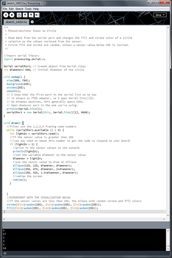
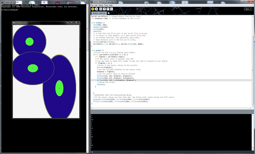
Week 12: Interface and application programming Goal: write an application thet interfaces with an input &/or output device In the assignment of this week I'm going to use processing to visualize the data extracted from the Hello.Light board made in the assignment of Inputs. This board has a photoresistor and throws the data through the Serial connection to the computer. What we do with processing is to use this data as variables that allow us to make a visual that will change while the light change on the board. The first thing I do is check that processing identifies correctly the Serial Port in the computer. To do this I used the code designed by Tom Igoe that you can find here. Pulse Run and processing console show us the Serial Ports available in my computer (this happens because we use the println command to print the data we ask, in the console) will appear. Code by Tom Igoe :
In my case the Serial Ports are COM3 and COM8. If you want to check in which one the board is plugged through the FTDY wire go to windows device manager (if you work with windows like I do) and what is the correct port, in my case COM8. Now I can program the display of the data. I used this tutorial as base, created by Providence AS220. I used their Sketch 2 where with the extracted data are use to draw concentric circles whose diameter and color varies depending on the changing data.
Now adjust the reading speed to 9600 (last number of the SerialPort) and I modify the graphics I want to do. What I do is to place more circles in different positions and deformations that vary according to the data collected, getting a psychedelic image.
At the same time, as we have a println, we can see the data provided by the photoresist printed in the processing console, and how the change according to the light received by the sensor.
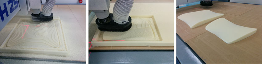
Week 11: Composites Goal: design and make a 3D mold and produce a fiber composite part in it.
Step 1: mold design and manufacturing
When de CAD design is made (using Rhino), I drill the mold in polyurethane foam.
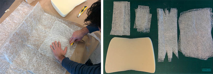
Step 2: preparing the fiber glass For adapting the Fiber Glass to the curved surfaces and prevent bubbles I make a pattern with the fiber glass as I would do with clothing to make a suit.
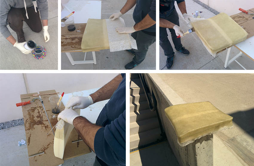
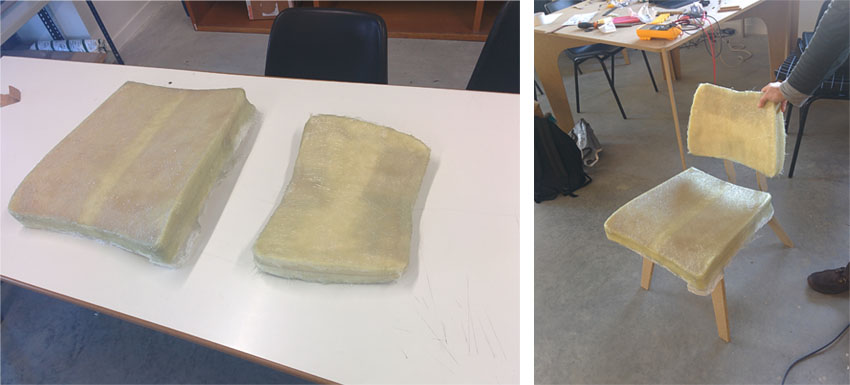
Step 3: preparing the composite I used a polyurethane resin purchased from Feroca that is already accelerated. It has two components, one is the polyester resin and the other one is the catalyst that will make the resin solidifies. The proportion of catalyst to be added is 1.5 % of the resin used . Working time before the resin catalyze is about 20 minutes. To apply the resin I used a brush. First I put a layer of resin on the polyurethane and then I put the fiberglass over it and give another layer of resin, being careful to avoid bubbles. I'm putting several layers to give consistency . In my experience I have seen that is better many small dimensions pieces of fiber instead of one large to improve the adaptation to curved surfaces . I worked on two pieces, inthe first one(the seat of the chair) I've only applied composite on one side , while the second piece, the back, I have done on both sides . The problem when applied on both sides is when you support the piece to apply the second side, the first one will take off and bubbles appear, so you must be very careful and apply all the resin holding the piece with a hand , still in points where it has been held small bubbles appear . May be better to apply only on one side and wait until the resin is dry and then apply the resin in the second side . Despite that the result wasn't bad.
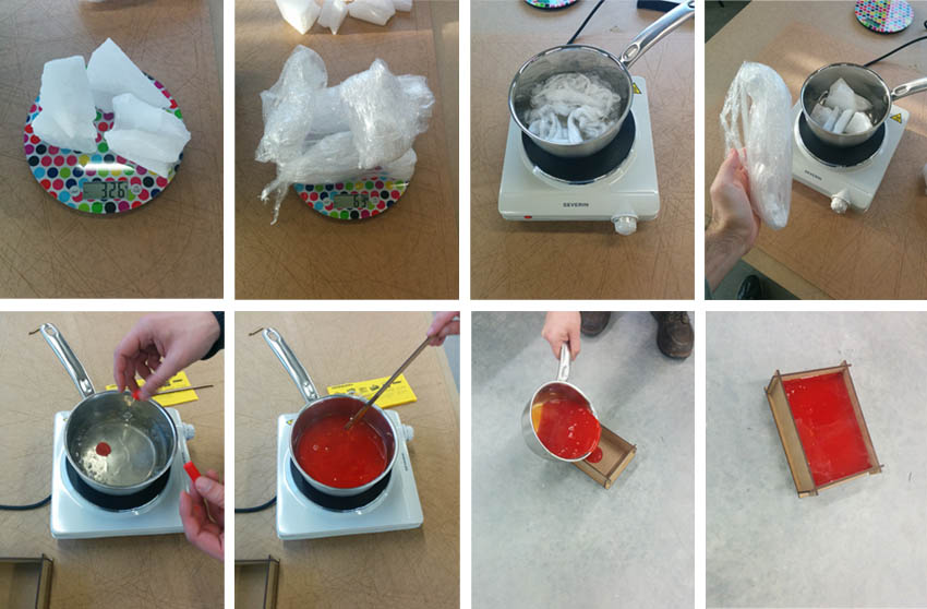
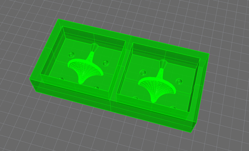
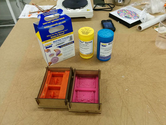
Week 9: Molding and Casting Goal: Design a 3D mold, machine it, and cast parts from it. Step 1: getting the machinable wax Let's get machinable wax from the following components: Paraffin, Polyethylene and crayons. Quantities : Pure paraffin. 320 gr. First, heat the wax until fully melted, then I gradually add the LDPE. I used the plastic used in the kitchen for wrapping food. Polyethylene needs more time to dissolve. PROBLEM: The amount of LDPEthat I have used is excessive, and the last parts of polyethylene have not dissolved properly. I read this problem appears spending 20% polyethylene or more in the mix, when the 15% is more than enough for a good result (in the FabLab we did the two mixes, mine just over 20% and my partner's with something more than 15% and his result was better). However wax didn't have problems for drilling. Once melted the LDPE I added a piece of wax crayon for getting the color we want. This last step is pretty fast, if you spend too much time the smoke starts to smell burnt. Then pour the wax into the form (I built one in DMF wood cut with laser with the dimensions needed) and let it cool. IMPORTANT: hot wax produces too much smoke and odors, work in a well ventilated area.
Step 2: designing the model in CAD
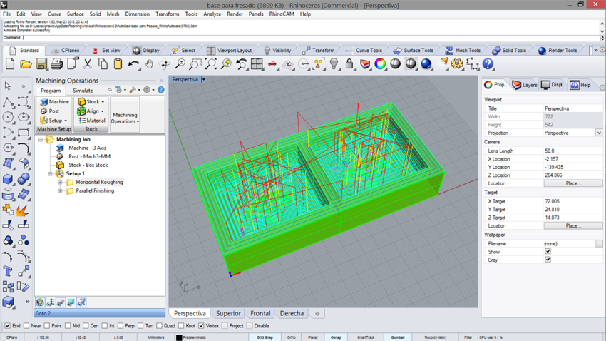
Step 3: Drilling the wax To mill the piece instead of the Modela I used large format drill machine because I wanted to try using RhinoCAM to set machining parameters. IMPORTANT: My piece of wax has shrunk too much in cooling process, so I have to pay attention to calibrate the Z axis because it is not the same in the center of the piece as in the ends. I have used a 3mm Ball Nose drill with speed of 1500 mm / min because all my surfaces are curved. The only flat surface is the juncture of the two countermoulds, so it is not important how the finish look in this part.
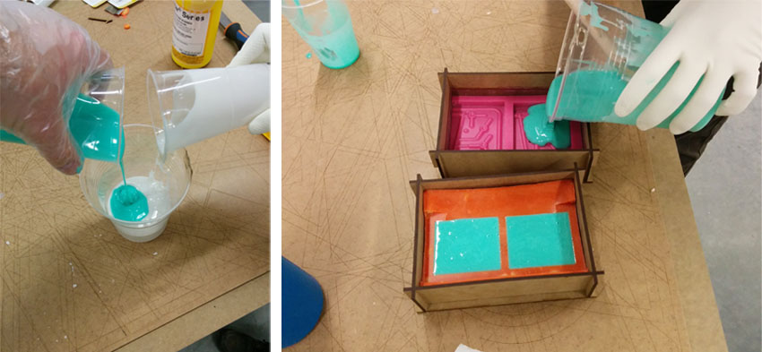
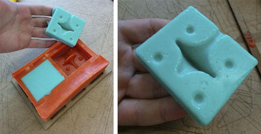
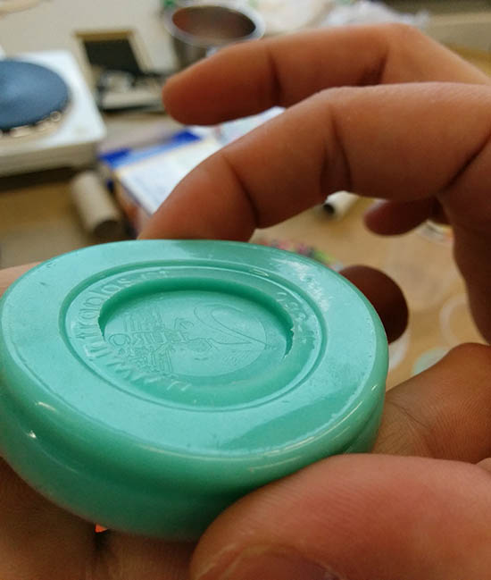
Step 4: Countermould in Silicone
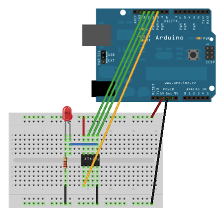
Week 8: Embedded programming Goal: Program your Hello board. For the assigment of this week I have used Arduino IDE as ISP for programming the Hello board with led and switch. Finally I could not complete the job because I have come to a standstill bug in Arduino IDE and I have not yet managed to solve. To make the assigment of this week I used as reference www.highlowtech.org tutorials and steps are the followings: First, I install Arduino from the official website and to connect the board to the computer. Once installed in the Device Manager (my OS is windows) check which serial port is installed, in my case COM 4. Because what I want is to program a ATtiny board, I download the drivers of ATtiny for arduino board. I can do it from the page highlowtech.org or from another website. To find out where to install, open Arduino IDE and go to Preferences, I can see the folder where I have to copy ATtiny files, in my case Documents> Arduino. Here I have to create a folder called "Hardware" and copy the downloaded ATtiny folder. Now restart Arduino and go to Tools tab> board. ATtiny board should appear . To start and check that the Arduino board is working properly and make sure the computer recognizes the board, open the Blink Example Sketch and Upload it to the board (before this I check that the serial port is correct, COM4, and the board is right, Arduino ONE in my case). I can see that the sketch works right because the LED flashes in the Arduino Board. Knowing that the board is working correctly, I open the Sketch Example called Arduino ISP and upload it (COM4 port plate Arduion UNO). Now arduino board is programmed to run as ISP. Now I connect the Arduino board to my Hello + led board through the 3x2 pins wire. I change the presets, Port keeps COM4 but board is now ATtiny84 (20Mhz), and the Programmer is Arduino as ISP. I choose Burn Bootloader in the Tools Tab and got the first error message. Also I try to push a program to see if it works, for this, open the Blink sketch and upload it, the presets are COM4, Board ATtiny 84 and Arduino as ISP, and I get the Following error message: avrdude: stk500_program_enable(): protocol error, expect=0x14, resp=0x50 Looking for what the failure means in internet, I find the problem is that the computer does not recognize the card correctly. This can be for two reasons: 1 - that the board is not located in the correct port, this is not my case because the device manager recognizes it correctly and I was able to program the Arduino board with Blink sketch properly. 2 - The board is not properly selected, which neither my case.
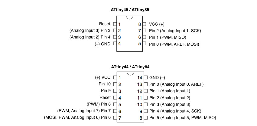
The scheme of equivalences between ATTiny pin 45 and 84 is as follows:
Once connected, I change the pin where the LED is connected. In the example sketch it is on pin 13 and in my case it the correct pin is 9. Now I upload the programming, with COM4, ATTINY84 board (now with 1Mhz becauso is not conected to a external 20Mhz Crystal), and Programmer Arduino as ISP as presets, and the error message is the Following: avrdude: stk500_program_enable(): protocol error, expect=0x14, resp=0x50 Now I'm still trying to find a solution and to program the ATtiny.
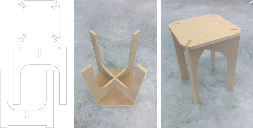
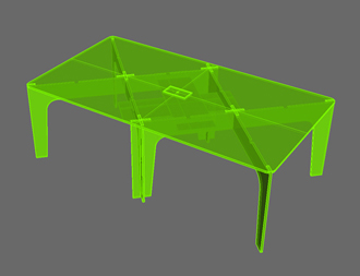
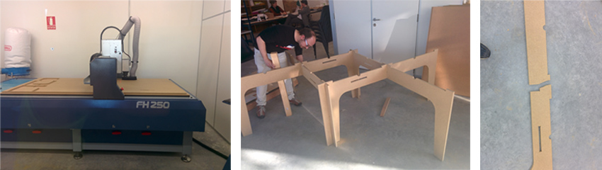
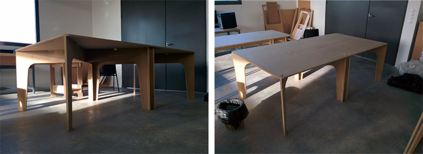
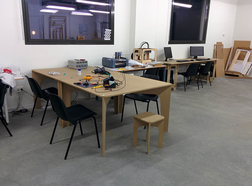
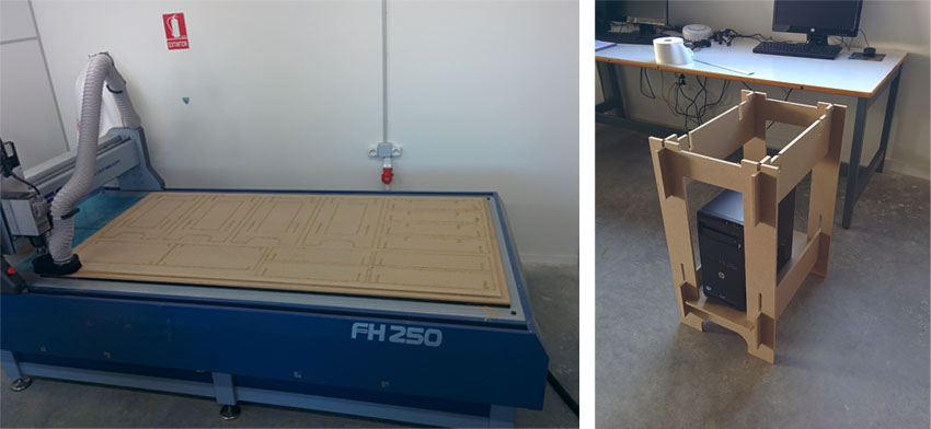
Week 7: Computer-Controlled Machining Assignment: make something big Goal: make two pieces of furniture that we can use in the Lab using milling cut without glues or fasteners, the piece must be stable by design. This weekly assignment has been made half to half with Ignacio Prieto, instead of making a piece of furniture each, we made two between the two. The material we use to make the furniture is wooden planks of MDF 16 mm thick. Machining has been made with a medium format CNC milling Alarsis FH250M, cutting dimensions 2,44 x1, 22 meters. We have used a 6mm diameter End Mill. First try, testing joints Before making the final furniture, we test the system making a stool, make by two pieces in X and a top board for sitting.
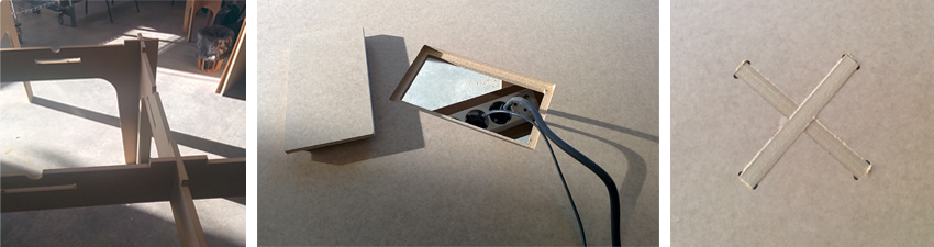
The system consists of adjusting joints to prevent movement of the parts and provide stability. The tolerance given to the joints was 0, so the assembly is more difficult but the parts remain fixed without using binder or screws. The result of the test is a stool which is stable even when you stand on it.
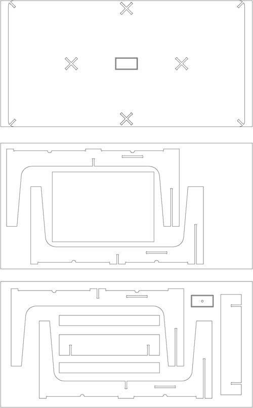
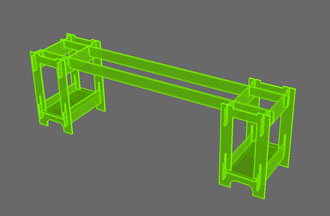
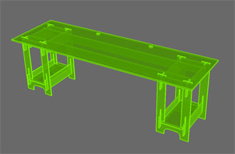
First Furniture piece: worktable This first piece of furniture is a worktable for using in the fabLAB where the top board is supported and serves as an anchor on six legs formed by four pieces that intersect each other to provide structural stability to the table. The board achieve to stiffen the assembly and give horizontal stability.
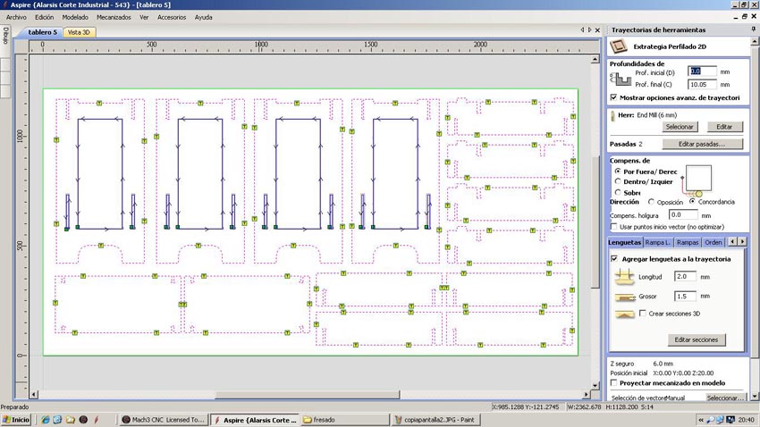
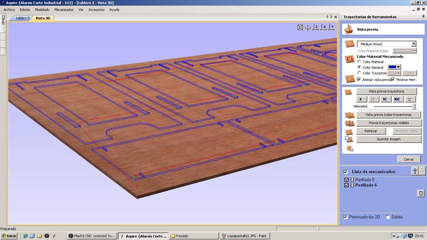
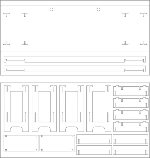
The software used by the CNC Machine is the Aspire. In the example images given, the pattern match to the second piece of furniture, but the cutting parameters are the same except for the thickness of the material, instead of 10 mm is 16 and and the number of passes is 3 instead of two. The first thing we do at Aspire is to define the dimensions of the material (2.44x1.22 meters) and thickness of 16 mm. Import pattern cut from CAD in .dxf format and now we choose how to cut each line, selecting, indicating the depth of cut, if cut outside, inside or over the line and add tabs to hold the parts while cut and prevent movement and mill break.
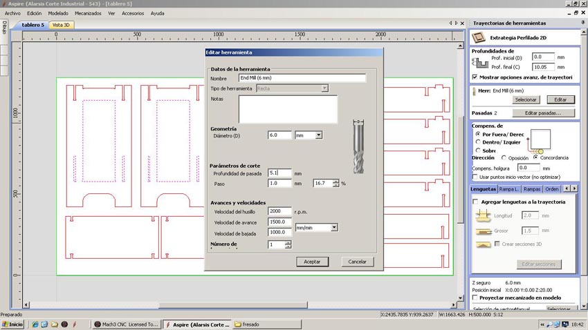
We select the tool that we will make the cut. In our case it is a Mill End 6 mm in diameter. It is important to select the right tool because in our design the corners have been done with a tool 6mm thick. The Mill expels chips compressing down and preventing cut pieces move. The speeds chosen were 1500 to advance with a depth of 5.4 mm to make the cuts in three passes.
After selecting all the cutting parameters we check that the machining is what we want (the image shows the machining of the second piece of furniture, which has only two passes because the material thickness is 10 mm) and export the G-code in .txt format. The code associate parameters for all the motion vectors and machine speeds, etc.
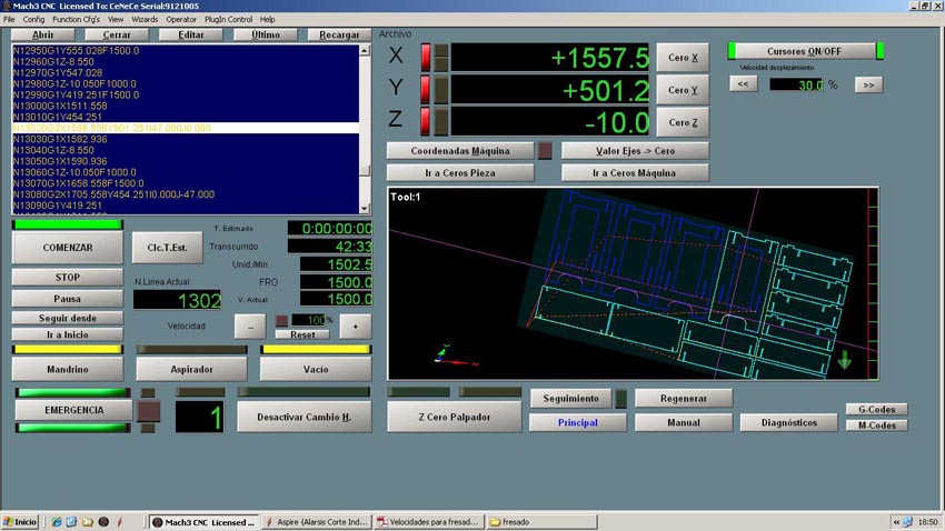
Open the G-code into the machine controller. We use the Mach 3. In this controller we calibrate the 0,0,0 point in the material and we are ready to start milling.
After milling we make the first assembly and discover a design mistake, the junctions are so narrow that avoid some of then turn to get the right position. When assembly we did too much force and break a piece. The solution was easy because of changing the direction of one union is easily mounted without problems. Also assemble the top board and we have the finished piece.
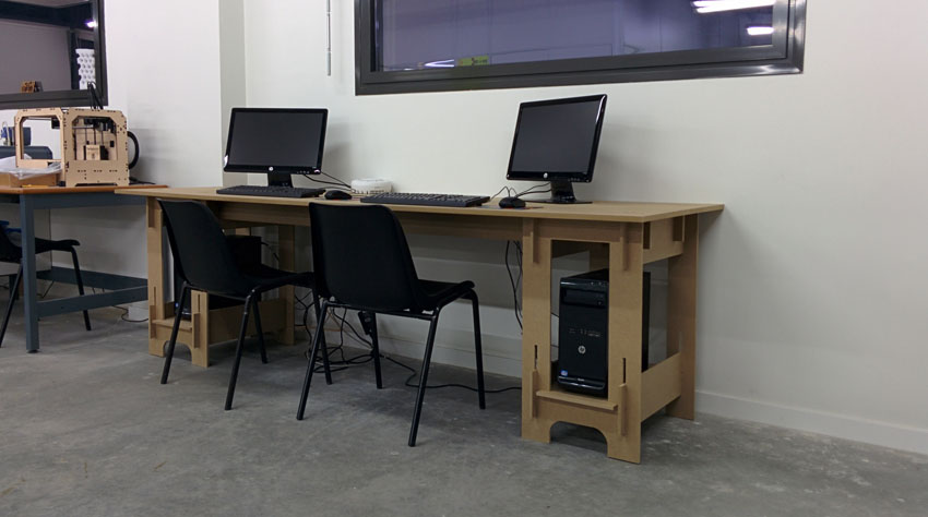
Second Furniture piece: computer desk Now let's do the second piece of furniture consisting of a desk to place the two computers for public use we have in the FabLab. The assembly system is very similar to the previous table, but the board used is 10 mm excluding the top board and the two beams that are 16 mm thick for added structural stability.
We perform machining of parts with the Aspire software and cutting with the Mach 3 as we have seen with the previous model.
|

Week 5: 3D scanning and printing
Goal: design an 3d print and object | 3D scan and object
FIXING THE CLAMPING PIECE OF AN UMBRELLA I use the assigment of this week of scanning and printing a 3D piece, to fix a broken umbrella I have in my office. It has two broken pieces that join the textile with the metal bar. The process to follow to fix this part will be to scan it, edit the design on the computer and print it in 3D.
|
 |
STEP 1: Separate the broken part of the umbrella and scan it in 3D
 |
First to do is get the broken piece, separating it of the umbrella to scan it. For th 3D scanning I use the Roland Modela MDX-20 wich serves both, as 3D scan and milling. This type of scanner has the limit of scanning by points, and only those accessible in the Z axis, so the holes of the workpiece will not appear in the digital model. After getting the scanned points, the software make a reconstruction, generating a mesho formed by the scanned points. To make the scan I used Dr. Picza software, provided by Roland.
|

In the software we chose the scan area to reduce the scan time by limiting the area where the piece is placed. As my piece is small, the limits are 45 mm in Y axis and 35mm in X axis.
Now regulate the separation of the steps in X and Y to detect the scanned points. The problem with this type of scanner is the time it takes to perform a scan. A closer spacing means more accurately but more time scanning. For such a small piece (45x35x15 mm), making separation of 0.3 mm step, the scan took more than 4 hours!!! So I finally chose a 0.5 mm step and the scan spent 1 hour.
To reduce the scan time I manually indicate in the software where the highest point in Z axis is to avoid wasting time scanning air. In my case this point is in 17.5X 22Y coordinates.

Problem: In the first scan, I had problems putting the piece directly on the base surface of the machine because the scan sharp end did not come down to the base and I lost the lower part of the piece in Z. To fix it I had to use a base of 3 mm thick and so I got to scan of the entire piece correctly.
STEP 2: Edit the digitalized piece by CAD
Scanning the piece we get a 3d mesh that can be opened directly in a 3D CAD program. I used Rhinoceros 3D, opening the exported file from the scanner software in dxf file.
In the two images below you can see the mesh of the piece just as scanned, the scan imperfections and broken parts of the original part appear in the digital piece.
|
 |

I modify the scanned piece for three reasons:
- the scanned the piece has all the problems the original piece had, that is, we can see that it is cracked on top.
- The scanner used, only scan in the z axis, so there are parts that are not accessible to the scanner, so I'll have to draw them manually.
- The scanner works by points, making a reconstruction of the surface from these points placed in space. The problem with this is that sometimes this reconstruction will not correspond with reality, as happens for example in the holes, where to be an interpolation of the points will not be understood as holes but a convex surface so we drilled them manually using CAD
To operate well in Rhino, we transform the mesh to Nurb curve with the command MeshtoNurb Nurb by allowing a more agile and quick editing. Now modify the necessary points and using Boolean operations we can remove parts of the scanned object, to obtain the improved piece we want to print. Having the corrected and modified piece with the improvements we want, we can go to print in 3D and export in STL format. |
 |

STEP 3: Print the corrected object
For the 3D printing I use Makerbot Replicator machine with Rlicator-G software. In print options, I choose printing base in contact with the hot base of the machine (no raft) for better adherence of the piece, but with raft in holes to allow the machine to print it.
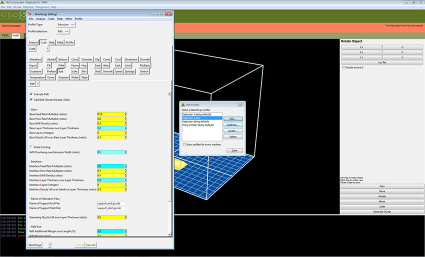
The piece is solid and Layer Heigh is 0.2 mm. I Generat the G code to print the piece.

Before printing, to check the Layers to print, I use the software Repetier where I can see exactly how each layer will be printed. In my experience, when Repetier show a problem with the layers, the machine reproduce the same problem.
Now that I know how the piece will be printed I can export the G-code to insert the SD card in the machine.

To improve the adhesion with the hot base of the Replicator and avoid the detach of the piece while is printed, smoothly I sand the teflon base and add a bit of ABS plastic diluted in acetone. Thus the new piece adheres better and does not detach during printing. |
 |
Now I have the new fixed piece to put it on my umbrella.

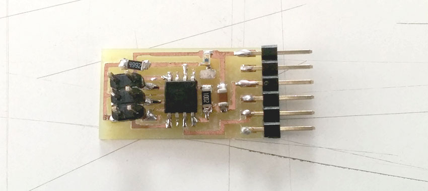
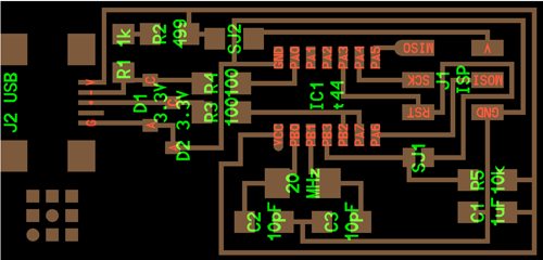
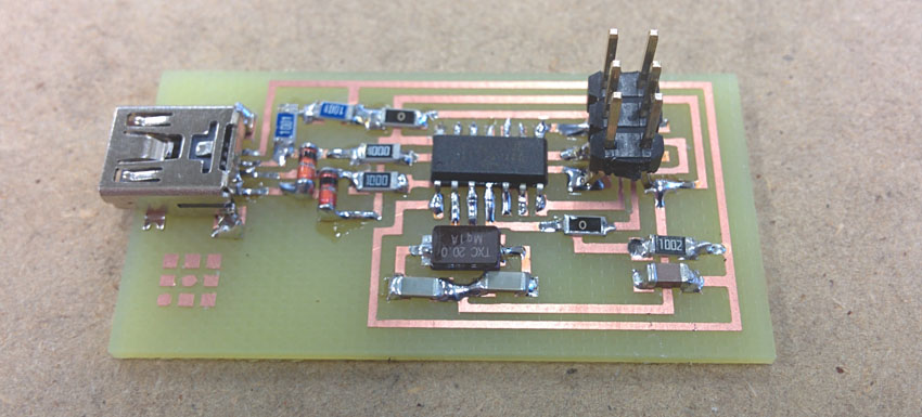
Week 4: Electronics Production
Goal: make the FabISP in-circuit programmer
This assignment has two steps, first to make the board and the second one to program the board.
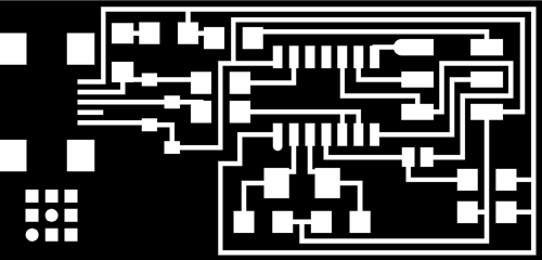
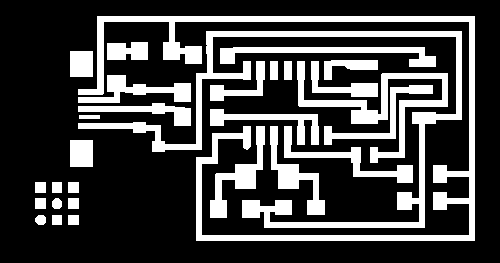
Step 1: Making the board
As reference files I used the files provided in the week 4 class for milling and program the board.
board: traces: |
For milling the board, I use the Roland Modela with a diamond drill 0.6 mm in diameter. I use Roland's software for engraving and cutting plate, Dr.Engrave. The problem I have is the software does not calibrate well the cutter diameter with paths, so you need to pay close attention because in the places where the black surface is less than the diameter of the cutter the software don't drill the board, so before machining we have to review the file to correct the errors and have a correct machining paths otherwise the paths will be in contact with others in the points where they have not been cut.
|
The main problem with the Dr.Engrave software is the offset of the first path is not accurate and makes smaller the circuit connections, sometimes even eliminatethem and avoid the conductivity between parts of circuit. Here are some examples of boards where I had these problems.
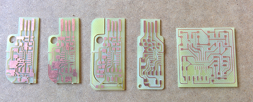
To fix that, I have done is to make wider paths using Photoshop, so I make sure that there will be connected the dots. Not a great solution but it is effective. In the future I'll try to use FabModules, but working on the windows, Dr.Engrave was the fastest option.
Now I drill de board and weld the components.
 |
 |
I have already made the FabISP, now I have to program it. When I connect it to the computer, this recognizes it as an "Unknown Device", this is correct because the FabISPis not yet programmed.
Step 2: programming the board
This step has been especially difficult for me because I found a lot of problems that took several weeks to resolve and I have delayed the others assignments with circuits .
My first problem is that we are a new FabLab that opened this year and we don't have a previous FabISP which program with and did not have any other programmer . We tried to enter the code using Arduino as ISP but it is not possible because the Bootloader Arsuino IDE is not c code.
Finalment we got a AVRISP v2 programmer and I started programming my FabISP it by following this tutorial. I installed AVR DUDE to enter the code on the board and downloaded the Firmware and Drivers for my computer to recognize the FabISP .
As I do not use one FabISP as a programmer , but a AVRISP2 , at the beginning is not necessary to install the drivers for the FabISP, but I'll have to install the AVRISP2 drivers for the computer recognizes it and can use it as a programmer . Once I have programmed my FabISP, then I should install the FabISP drivers for the computer recognize the board.
Now connect the computer to the AVRISP2 with an USB and my FabISP also in order it can get energy. Both boards must be connected by a 3x2 pins wire.
I open the windows console to start programming . If I want to check that AVRDUDE is properly installed I write in the console "AVRDUDE" and I appear all the available commands. Now I go into the folder where I downloaded the firmware and I can start.
First type:
| make clean |
and show:
c:\Users\FabLab/Desktop/firmware>make clean |
after that type:
| make hex |
and show:
c:\Users\FabLab/Desktop/firmware>make hex |
And then:
| make fuse |
problem: although the crystal is 20 MHz, the programming must be at a frequency of 1/4 of the crystal, at first I was programming with the programmer working at 20 Mhz and had an error in the Fuse. Finally I got into the drivers of the programming and I reduced to 5 Mhz. After that, everything worked correctly when I made the Fuse:
c:\Users\FabLab/Desktop/firmware>make fuse avrdude -c avrisp2 -p attiny44 -U hfuse:w:0xDF:m -U lfuse:w:0xFF:m |
finally, the problems appear:
| make program |
and:
c:\Users\FabLab/Desktop/firmware >make program |
After verifying the connections are good and that there is continuity in the circuit, I install ATMEL STUDIO to verify the board.
Connecting the FabISP, Atmel Studio is able to recognize the microcontroller I am using an ATtiny 44, but is unable to identify the other components (or the crystal), so surely there is a problem with any of them.
After reviewing everything thoroughly, I found the capacitators placed close crystal are not the value they should be, they are 100pF instead of 10pF. Unweld the wrong capacitators and weld the right ones. Atmel Studio now recognizes the components of the board.
I get back to the console windows and Firmware folder and repeat the last operation:
| make clean |
| make hex |
| make fuse |
finally:
| make program |
and...
c:\Users\FabLab/Desktop/firmware >make program avrdude: AVR device initialized and ready to accept instructions |
Now I have the FabISP working!!!
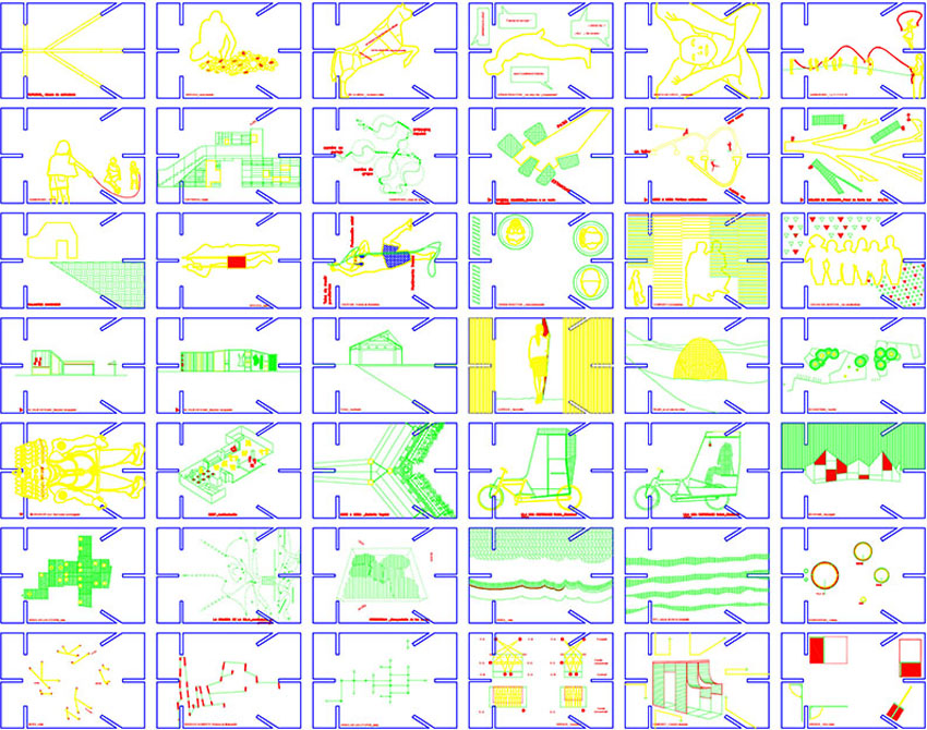
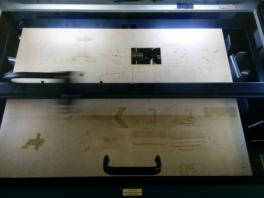
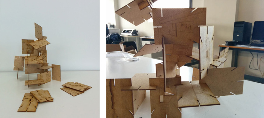
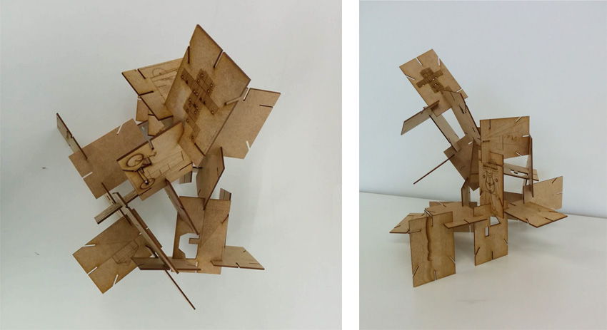
Week 3: Computer- controlled cutting
Goal: design, make and document a press-fit construction kit
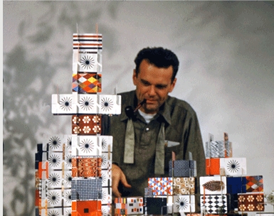
"HOUSE OF CARDS", REVISITING EAMES'S WORK My work this week to make a press-fit kit is based on the toy cards designed by Ray and Charles Eames in 1952. The main changes with the original model have been customizing the cards using laser engraving and cutting for transparency effects and drawings in cards. Also a modification of the position of the anchor holes allow a free-standing and organic result in the final model. The material used in this New house of cards is 2mm thick MD wood, worked with laser to cut and engrave. |
 |
Template sheet:
The CAD software used to design the cards was AutoCAD, This is the drawing template used for cutting
Cut Parameters:
I used three cutting parameters divided into four layers. One for vector engraving (green layer), with power 100 and speed 50 , Other for raster engraving (red layer) with power and speed 100. And for inside and outside cuts (yellow and blue layers) a power of 100 speed of 5.
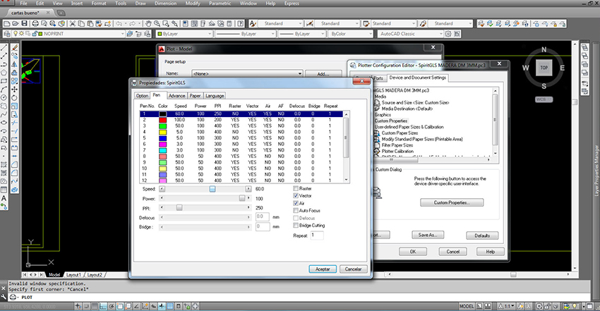
The laser machine we used in the FabLab UPM is the Spirit GLS with 80 Watts. Its work surface is 960 x 610 mm.
And the results:
Week 2: CAD
Goal: Get a CAD design for our Final Project
The design is based on getting a skin which expands and contracts to reduce its size a third part by folding its faces.
The work involves parameterize the surface using Rhino and Grasshopper, from the surface triangulation and by folding and unfolding the faces we get the motion needed to reduce the surface.
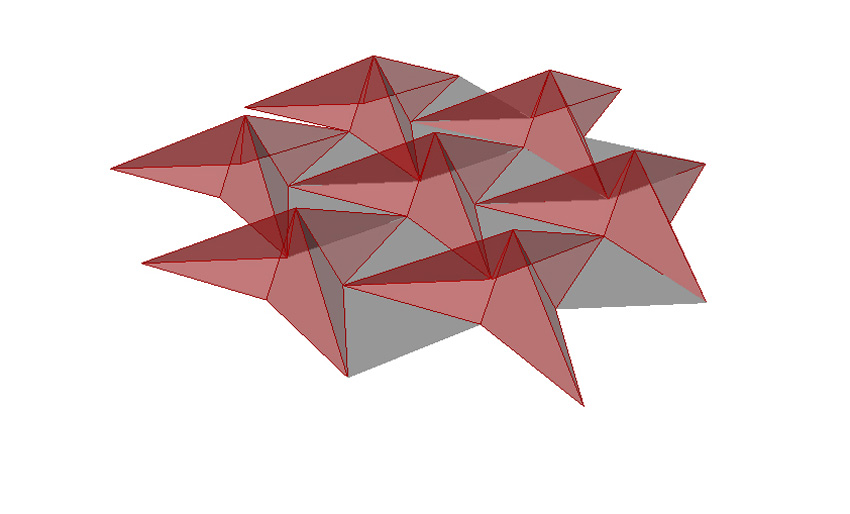
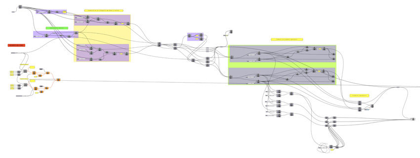
Grasshopper definition:
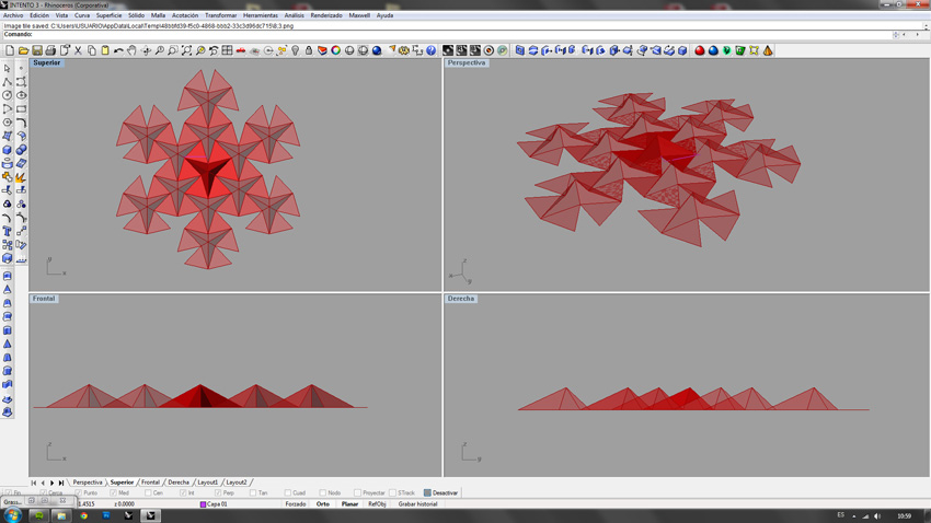
Rhino results:
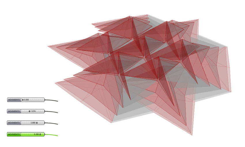
Expanding and contraction of the model changing the initioal parameter:
Week 1: Introducing the Final Project
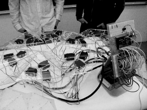
Goal: get a customizable and variable space, sensitive to what happens around . Build a changing and dynamic architectural model that is transformed according to environment conditions change .
The project is based on three main steps:
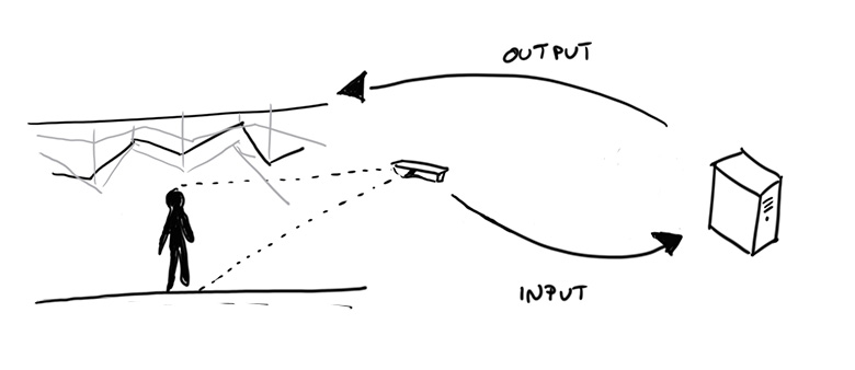
1 - digitization of the space through a 3D scan (using a device like Kinect) that allows us to get digital real-time data from this physical space. 2 - use the data collected to transform the model designed, using a parametric CAD software (Grasshopper type) that allow the modification of the design according to the changing initial conditions . Thus, the data collected by the 3d scan are the initials the parameters and variables that will transform the space designed by CAD . 3 - Connect the digital model to a physical mechanism, built using digital manufacturing tools in the FabLab and make their shape change according to the outputs change from the parametric processing. |
 |
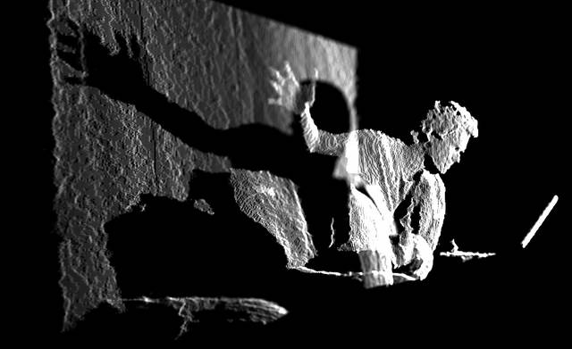 |
Digitization of space by devices like Kinect allows us not only to know in real time what happens in the physical space but also to use it as initial parameters that will transform the final model, creating a continuous feed of data whom the surface answer adopting different shapes.
|
Here I give you two examples of projects that works with the transformation of surfaces in a similar way as I do. The first, PixelSkin is a surface facade based in equilateral triangles that regulates the entrance of light into the building. The second example, Responsive Kinetics, is a project focused on the mechanical deformation of a tessellated surface in response to temporal variations of elemental forces. The surface changes With the light, air, and precipitation from outdoor to indoor conditions. I insert two videos you can see the two projects in motion.
|
PixelSkin by Sachin Anshuman |
|
Responsive Kinetics by Anthony Diaz and John Hobart Culleton |