5. Electronics production
THIS WEEK CHECKLIST
- [✓] linked to the group assignment page
- [✓] Documented how you made (mill, stuff, solder) the board
- [✓] Documented that your board is functional
- [✓] Explained any problems and how you fixed them
- [✓] Included a ‘hero shot’ of your board
Group assignment
This time, I work with my groupmates together to Characterize the design rules for your PCB production process: document feeds, speeds, plunge rate, depth of cut (traces and outline) and tooling. CLICK HERE for the detailing of group assignment page.
Warning
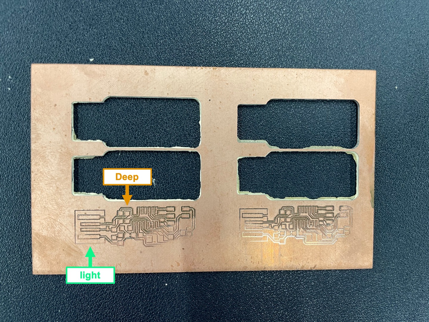
You can see the upper part of the PCB, line is more deeper. For the lower part, line is more lighter. It is because I didn’t lock up the mill bit. Mill bit was loosen when it operated. Therefore, you need to remember to lock up the mill bit brefore operation.
The other problem is about putting the double side tap at the back of PCB is not flat enough. Therefore, when machine milling, the mill bit may not have a good touch with the copper plate. Please pay attention when you puuting the double side tap or glue at the back of PCB.
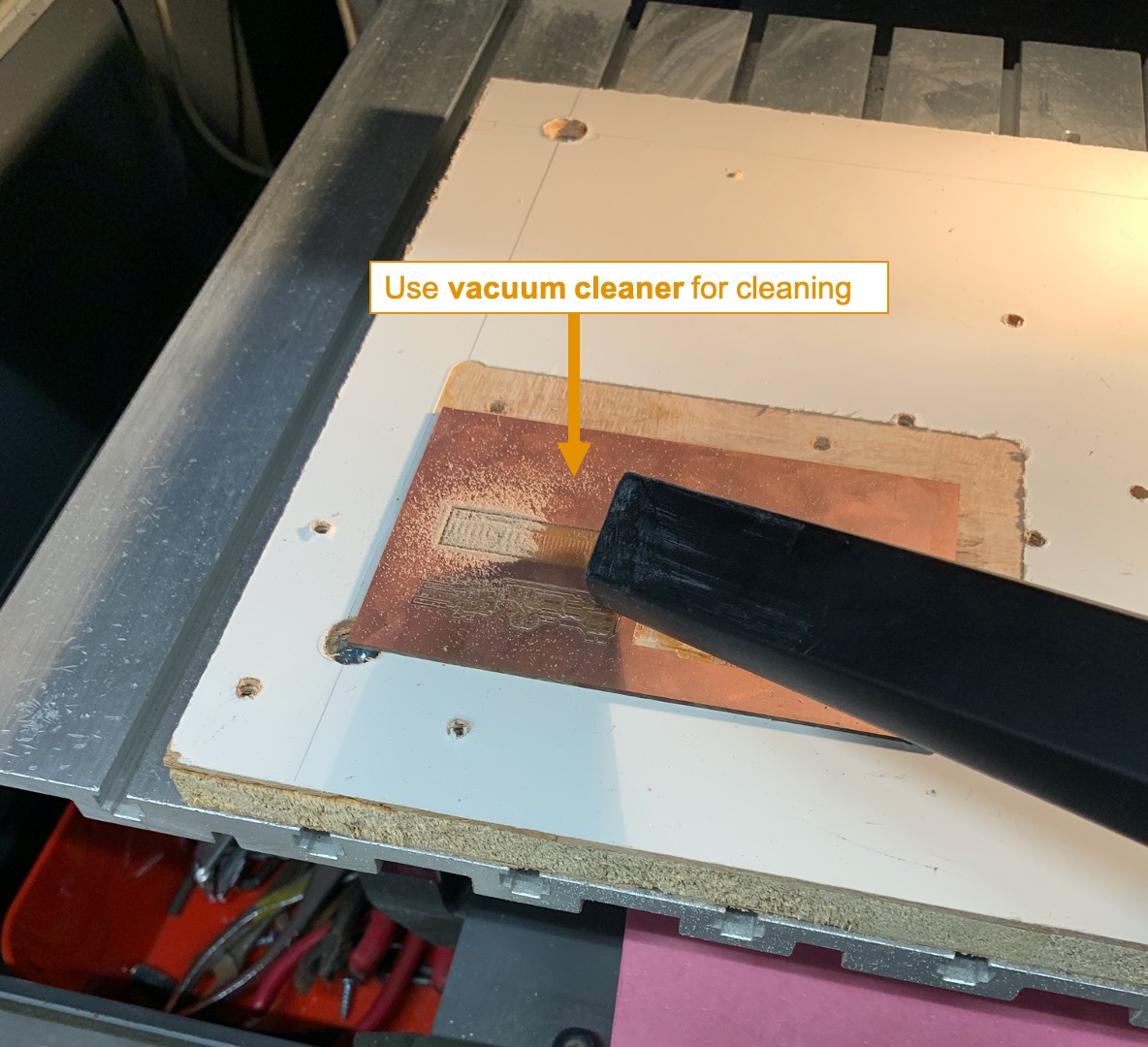
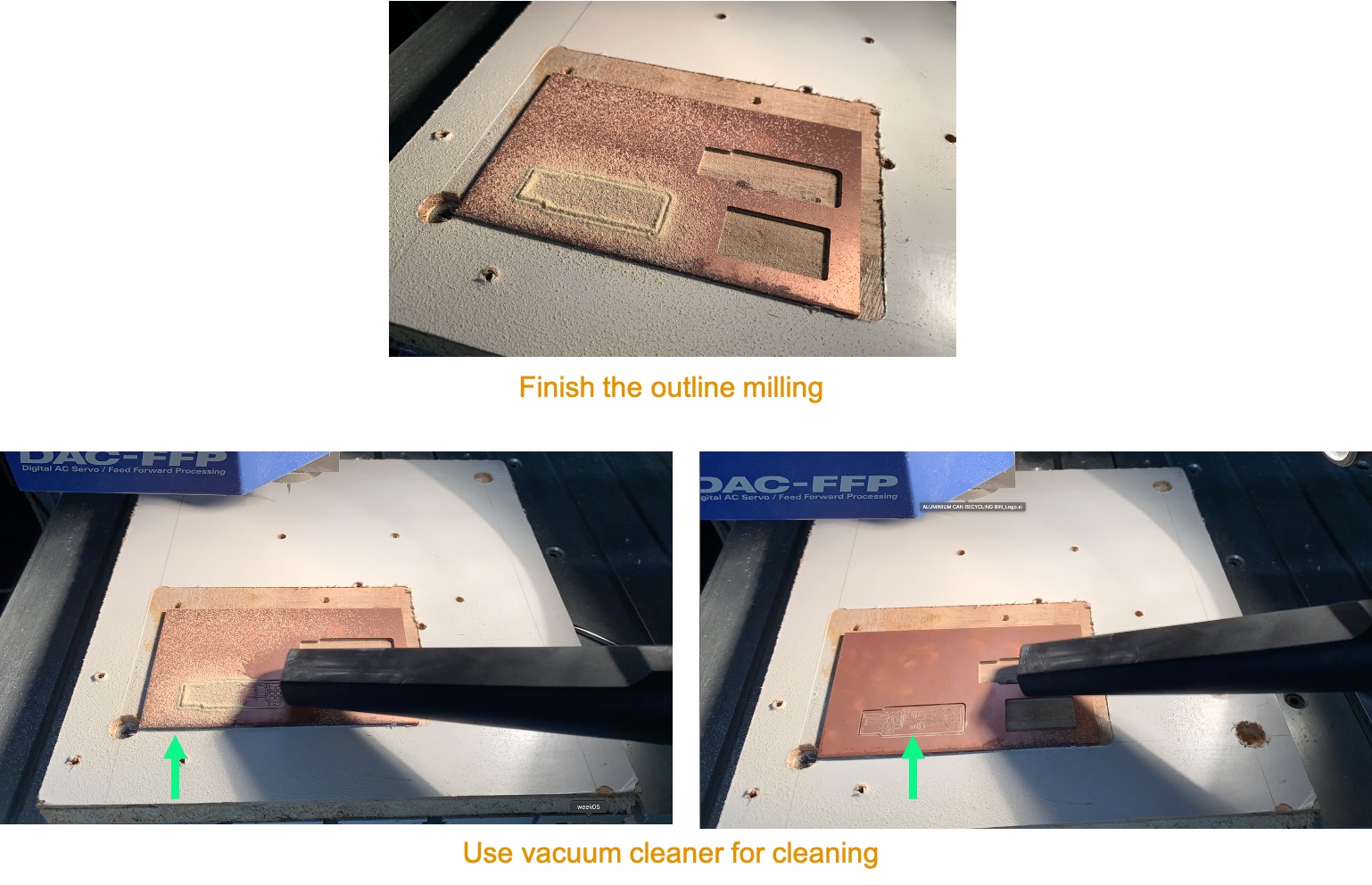
After finish the milling, I use vacuum cleaner for cleaning.
Individual assignments
1. Make an in-circuit programmer by milling and stuffing the PCB, test it, then optionally try other PCB fabrication process.
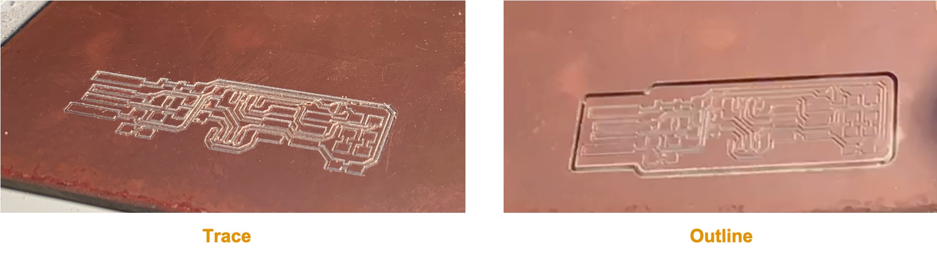
This is the result of milling trace and outline.
After finish the milling, I use vacuum cleaner for cleaning.
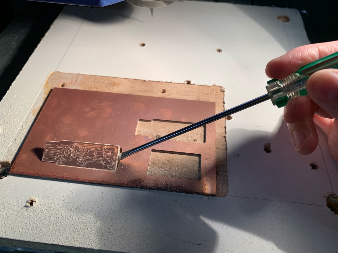
I use screwdriver for taking the PCB out.
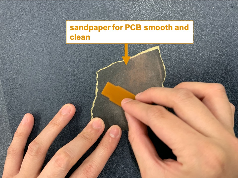
I use sandpaper for making the PCB smooth and clean.
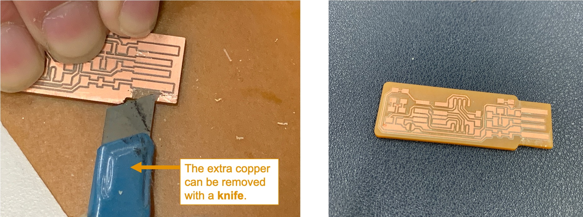
The extra copper can be removed with a knife (Left photo). Right photo shows remove all the extra copper. It decreases the situration short circuit when you stuffing the wrong components or wrong position.
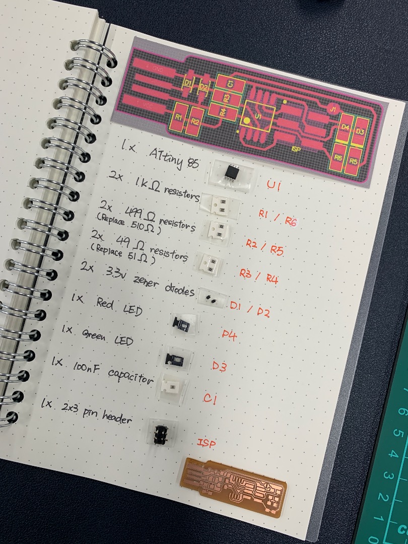
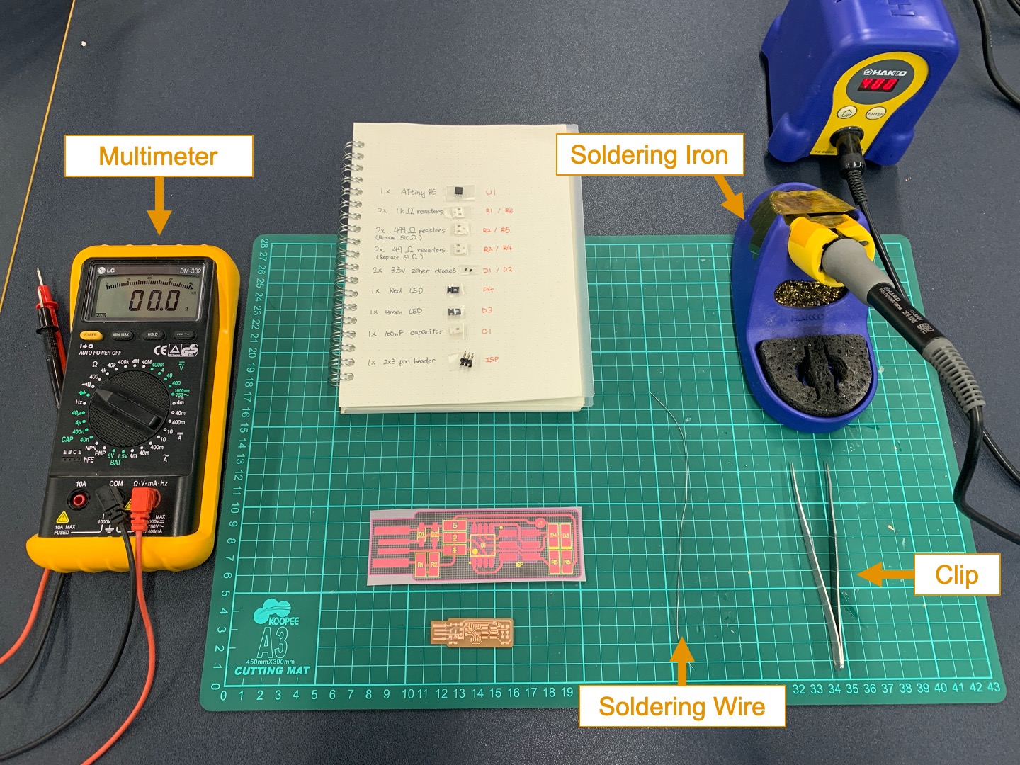
Since these all the components are very small. I paste, write down component’s name and position before Stuffing. I helps to have a clear picuture what kind of component need to go which position. Since some of the resistors cannot not be find in store, so German decide to buy the nearest value t replace that.
These are some tools when I stuffing. Using Multimeter to test the component is that have short circuit situation after stuffing. After you stuffing each component, I strongly recommend to test it before move on to next component. Since all the components are too small, using Clip to hold and put on the right position. The most important tool is solering iron and soldering wire to mount the component on the PCB.
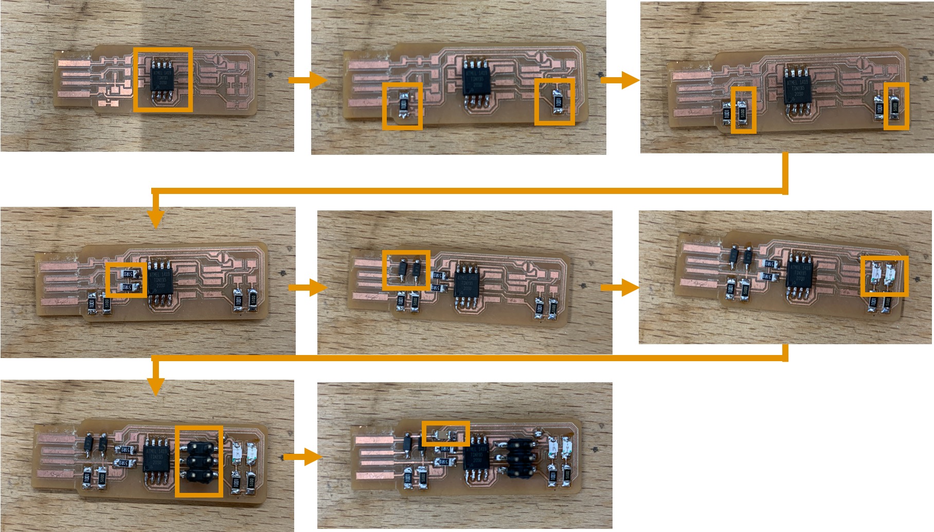
This is the process that I stuffing all components on the PCB board.
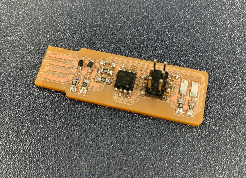
This is the final look after finished stuffing all components on FabTinyISP.
Click Here is a detail tutorial for software installation. Since the tutorial is highly recomended use Linux for software installation, so I decide to use Linux. Here are the steps for software installation.
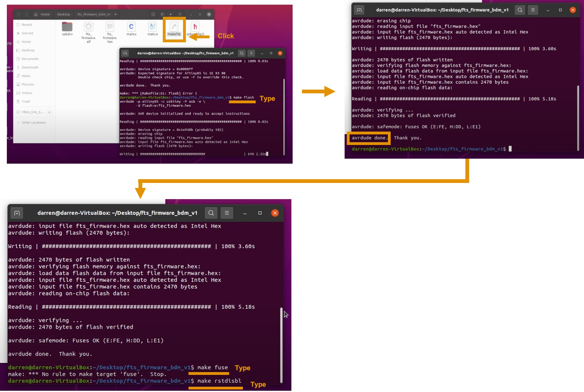
Here is the reult of though FabTinyISP uploading program to ATtiny85 PCB. It is successfully uploading the program.