5. Electronics production
Group assignment
Characterize the design rules for your PCB production process: document feeds, speeds, plunge rate, depth of cut (traces and outline) and tooling.
Individual assignment
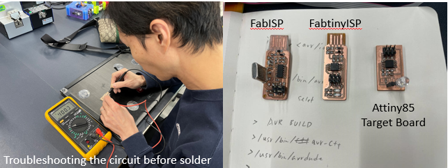
Learn PCB (Printed Circuit Board) production this week. FabAcademy assignment is very challenging. After four days of hard work, I changed from ATtiny44A FabISP to ATtiny85 FabtinyISP because upload firmware successful, but not effective! Try to upload firmware with win10 (not success), Mac OS (not success) and Linux OS (success). Finally, I also try use arduino as ISP and build another ATtiny85 tanget board to test the FabtinyISP. Althrough, I need to try man ymany time but it is very funny process for me.
Process Characterization: PCB production
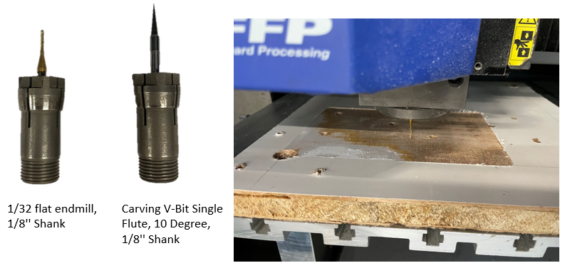
In the Fablab laboratory, we all choose Roland-MDX500 for machine milling. Although it is not suitable for mass production, it is convenient for rapid prototyping and is more environmentally friendly. The machine used for marking is a milling machine, a 10 degree Carving V-bit is used to engrave the circuit trace, and a 1/32 flat endmill is used to cut out the outer edge of the entire board.
Mill Test Traces

The fab academy test trace file above was use to create cam to test MDX-500 milling machine condition and satisfies the group assignment assessment requirements of: 1. Characterize the design rules for your PCB production process: document feeds, speeds, plunge rate, depth of cut (traces and outline) and tooling. 2. Document your work individually
1. Production method
Because I haven’t learned circuit design and components at this week. I chose the version “FabTinyISP Minimal” from - Brain. Brain provided the .png files required for PCB traces and cut out borders on his page. I just made it directly according to a downloader that has been designed. Before starting work, as a beginner, I need to take a closer look at this specific tutorial and video tutorial. Therefore, I only need to make a .NC file for the MDX-500 milling machine.
2. Material
I choose FR-1 for machine milling PCB Circuit board.
- 【Material】 Material: FR-1 copper clad laminate DIY PCB, Copper; Layers: Single-sided.
- 【Size】Dimension: 125x75mm(L*W); Thickness : 1.5mm.
Making the .nc file
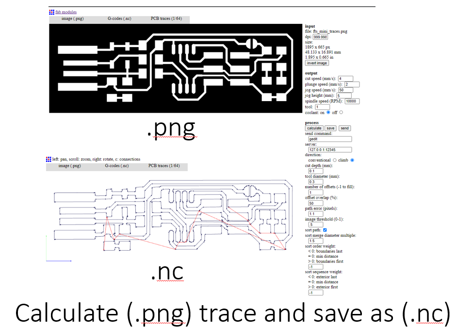
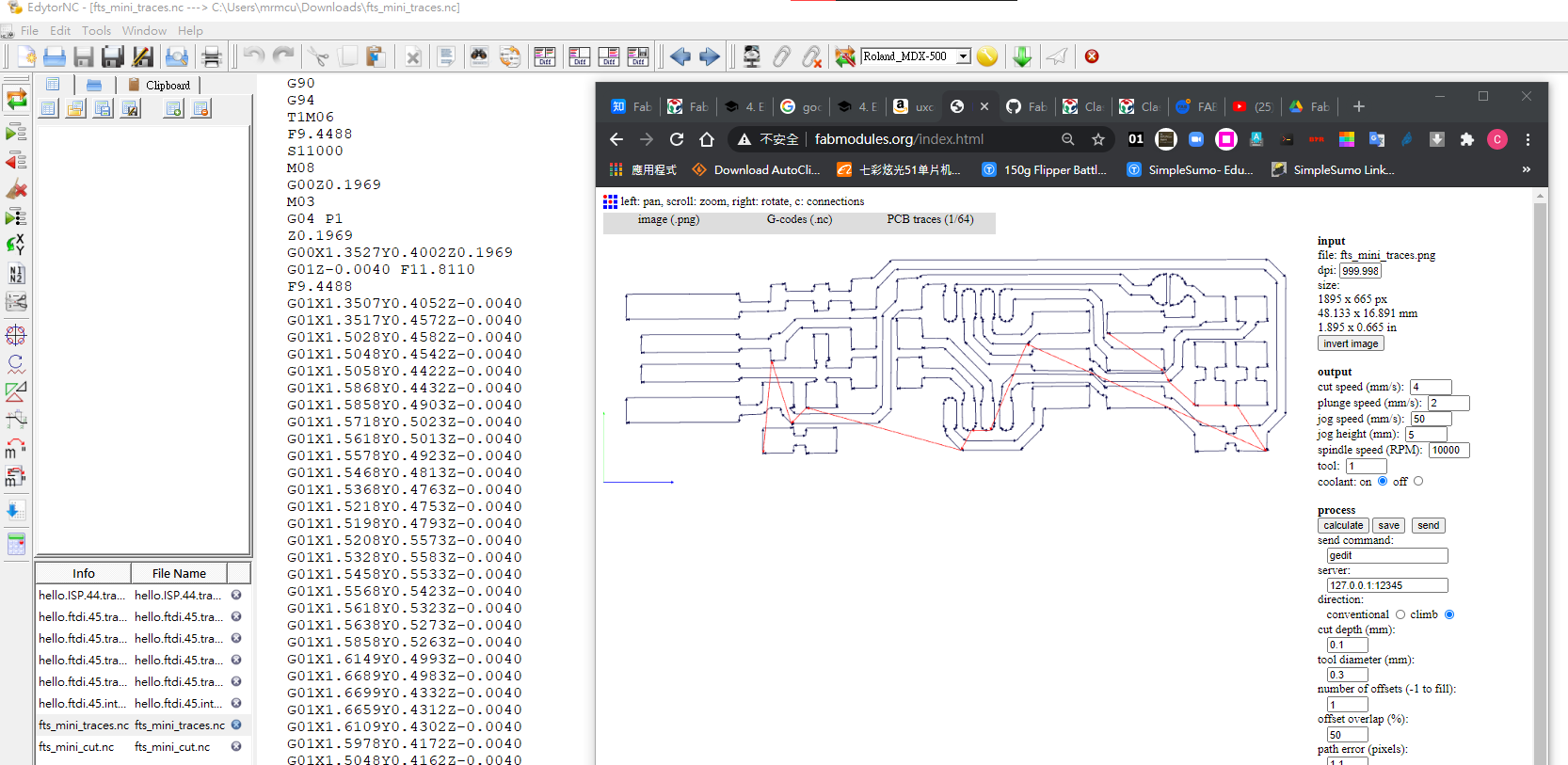
Convert the .png files to .nc using mods
-
Go to - Fabmodules
-
Select png file.
-
Select the process from process > PCB traces (1/64).
-
Select MDX-500 as the milling machine. Set the speed to 4mm/s and origin (x0, y0, z0) to zero and outputs to inputs.
-
Set the tool diameter (I used a 0.3mm flat milling tool), the cut depth to 0.1mm, the offset number 1 needed to clear the copper between USB pins, offset stepover number to 0.5.
-
Press the calculate button. Now save the (.nc) file
For producing the other file, the process is more or less the same.
3. Milling circuit board (PCB)
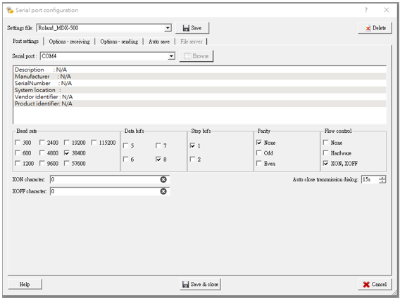
I used it to milling the circuit on the PCB board via edytornc send NC code. I choose this software because Roland-MXD is old machine over 15 years ago with serial port and no updated software suitable for win10.
Open NC file with edytornc
Milling steps
- Fixturing (using double-sided tape) –> Underlay (addition wood base) –> Orientation (target board) –> Zeroing (XY and Z) –> Lifetime –> Deburring (Filing) –> Cleaning
Adjust X/Y origin: The X/Y origin determines the start point on the flat PCB board. The X/Y direction buttons can be used to adjust the X and Y coordination of the milling bit. After reaching the ideal location, click Set Origin Point >> X/Y to set the current coordination as X/Y origin.
Adjust Z origin Z coordination determines the depth of the milling bit.
START TO MILL
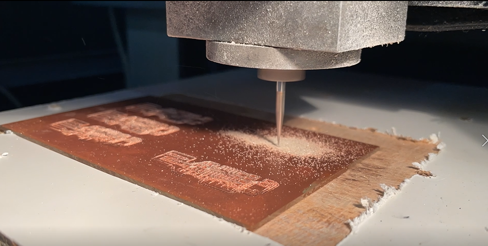
Then cut it and waiting.
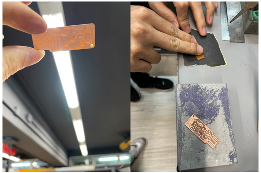
Observe the PCB under lighting check the milling quality. Deburring the surface keeping smooth and clean. The extra copper near the USB can be removed with a knife.
Soldering the Components
The biggest challenge this week is welding! I might not find it with a magnifying glass when dropped on the ground. I still took a breath - can these things be soldered?
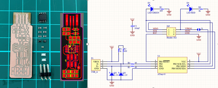
Using the components list to find the components
- 1x ATtiny85
- 2x 1kΩ resistors
- 2x 499Ω resistors
- 2x 49Ω resistors
- 2x 3.3v zener diodes
- 1x red LED
- 1x green LED
- 1x 100nF capacitor
- 1x 2x3 pin header
After experimenting several times, I figured out some experience:
- Put the tweezers first. Then put down the tweezers, pull the solder wire with your left hand and the welding gun with your right hand.
- Use the solder head to press a pin on the side.
- Put the end of the solder wire on the solder head.
- When the solder melts into a liquid state, remove the solder wire, and then quickly remove the solder iron.
- If the welding joint is ugly, you can use the welding head to melt it and add a little bit solder wire. First quickly remove the solder head, then quickly approach it, scrape it with a pointed tip and then remove it.
According to the image of - Brain’s version, to soldering it. PCB board look like beautiful, make it perfect.
Programming
Preparation :
Pasting several layers of tape on the back of the USB port to make it more suitable for insertion.
Functioning: Circuit Board
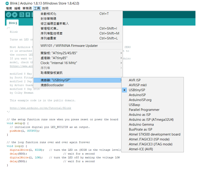
I programmed my first FabtinyISP board with the FabISP using Arduino IDE under WIN10 enviroment.
 void setup() {
 CLKPR = (1 << CLKPCE);
   CLKPR = (0 << CLKPS3) | (0 << CLKPS2) | (0 << CLKPS1) | (0 << CLKPS0);
 pinMode(2,OUTPUT);
   }
 void loop() {
  digitalWrite(2,HIGH);
  digitalWrite(2,LOW);
  digitalWrite(2,HIGH);
  digitalWrite(2,LOW);
  }
Blow the Reset Fuse
Congratulations, the ATtiny85 on the board has the code loaded onto it and is working correctly. There are two final steps left to turn my board into a programmer that can program other boards. I programmed my first FabtinyISP board with the FabISP under LINUX enviroment.
First, change the bit that will turn the ATtiny85’s reset pin into a GPIO pin. This will disable ability to reprogram this ATtiny85 in the future. Connect ISP programmer to ATtiny85 board one more time, and run make rstdisbl. This does the same thing as the make fuses command, but this time it’s going to include that reset disable bit as well. You should see some progress bars, and with that, avrdude will never be able to talk to this chip again through the ISP header.
$ avrdude -c tk500v1 -P/dev/ttyACM0 -b19200 -p t85 -V -U lfuse:w:0xe1:m -U hfuse:w:0x5d:m -U efuse:w:0xff:m
Second, disconnect VCC from the Vprog pin on the ISP header by removing the bridge on the solder jumper. Sometimes the excess solder will stick to a clean soldering iron tip; if not, use desoldering braid to remove the solder from the jumper, thus breaking the connection.
Test my Programmer
Now, I own my working ISP programmer! Following youtbe will show how to use my ISP to programming another ATtiny85 target board.
This is my testing programmed using my first FabtinyISP board to upload.