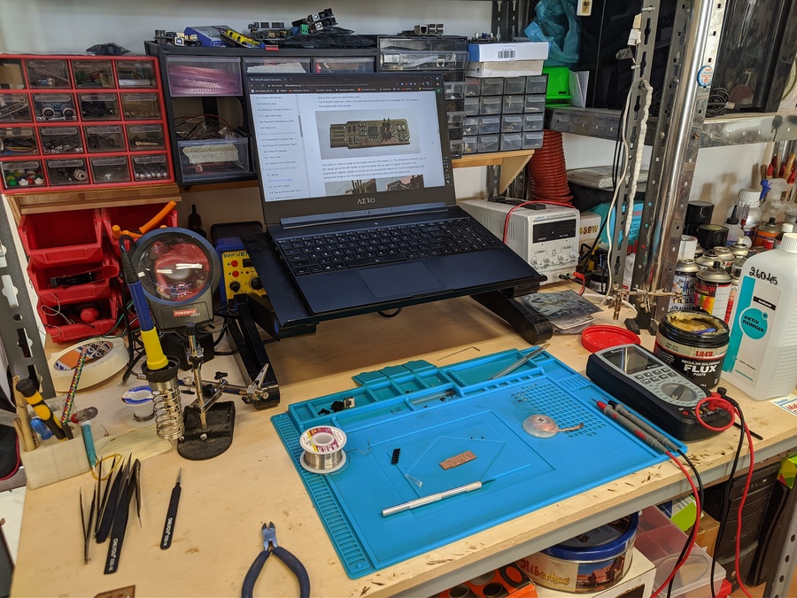
Electronics production
The machine
Milling machines that are capable of reaching desired accuracy for PCB production in my lab are Roland SRM-20 and MDX-40. I’ll be using SRM-20 for this assignment.
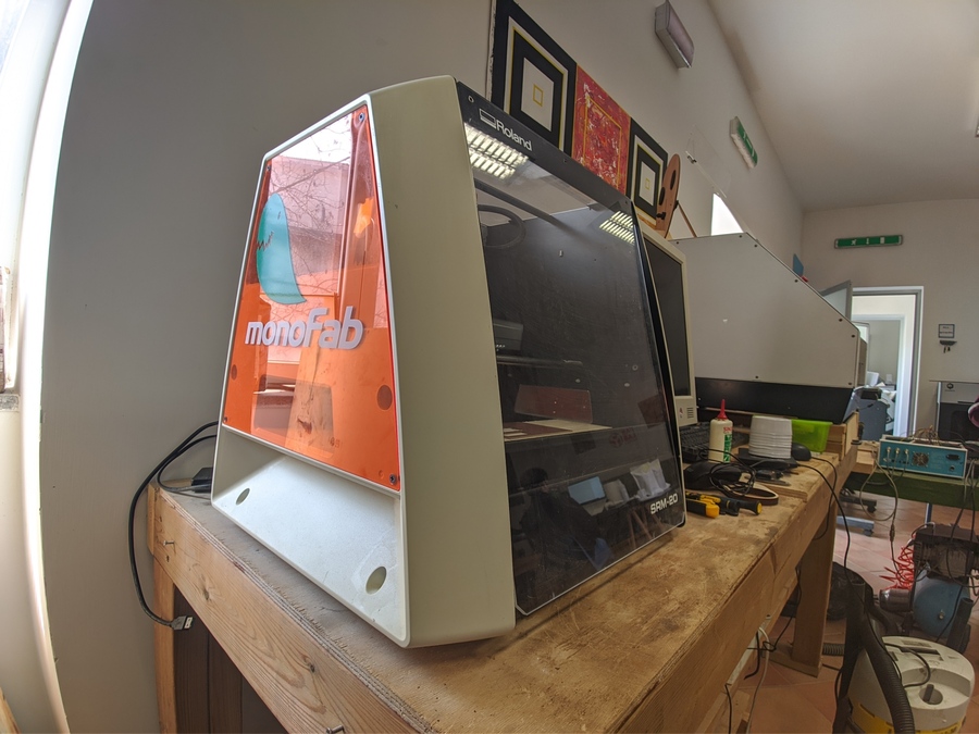
Specs
◤ Operation strokes xyz: 203.2x152.4x60.5mm
◤ Materials: Modelling Wax, Chemical Wood, Foam, Acrylic, Poly acetate, ABS, PC board
◤ From collet to table: 130.75mm
◤ Software resolution: 0.01 mm/step (RML-1), 0.001mm/step (NC code)
◤ Spindle rotation speed: 0 – 9000 rpm
Software
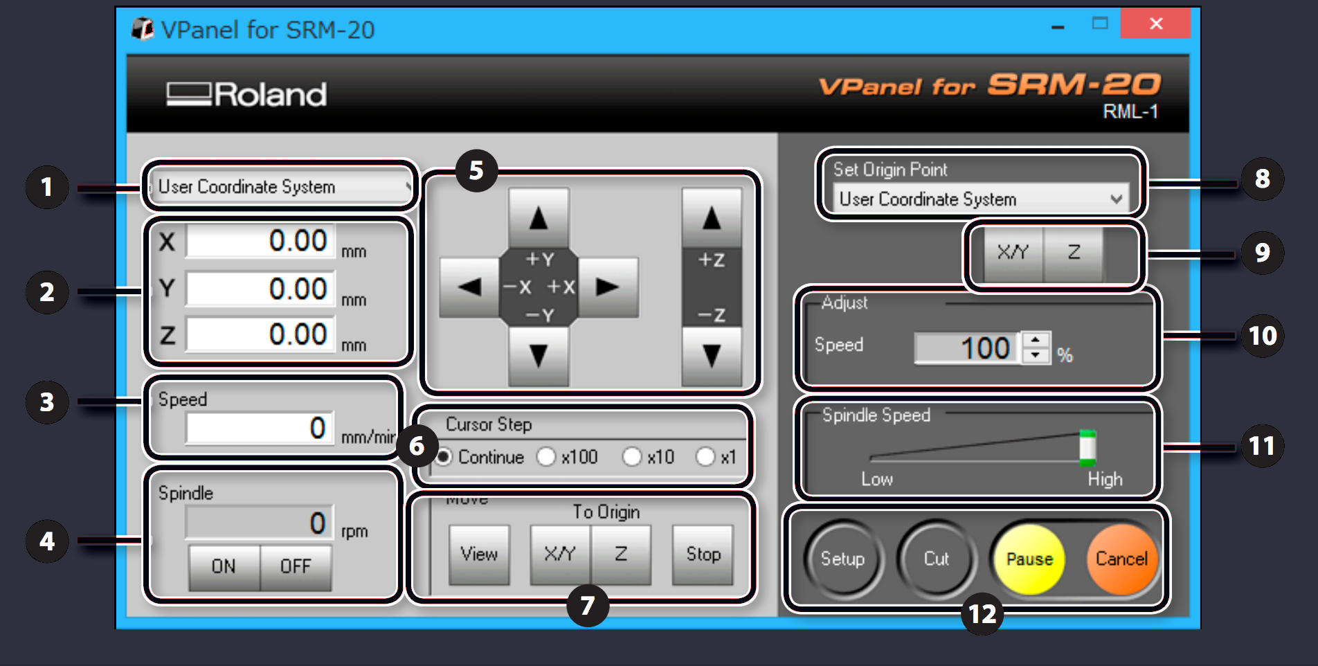
VPanel is a control software for Roland SRM-20
| 1. Coordinate system 2. Current coordinates 3. Current movement speed 4. Current spindle rotation speed | 5. Position controls 6. Movement step 7. Move controls 8. Coordinate system | 9. Set origin in X/Y and Z 10. Speed adjustment 11. Spindle speed adjustment 12. Operation controls |
Prep work
In order to achieve the best milling results ◆ The machine must be calibrated, lubed and clean ◆ The bit and the collect must fit together and be well tightened ◆ Sacrificial material must be glued to milling machine’s working table ◆ The surface must be cleaned to flat with a flat bit ◆ PCB plate must be glued flat on top of sacrificial material
Cutting test
Generating path
Traces path
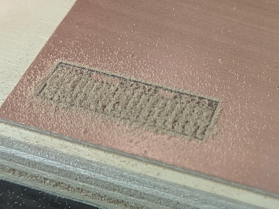
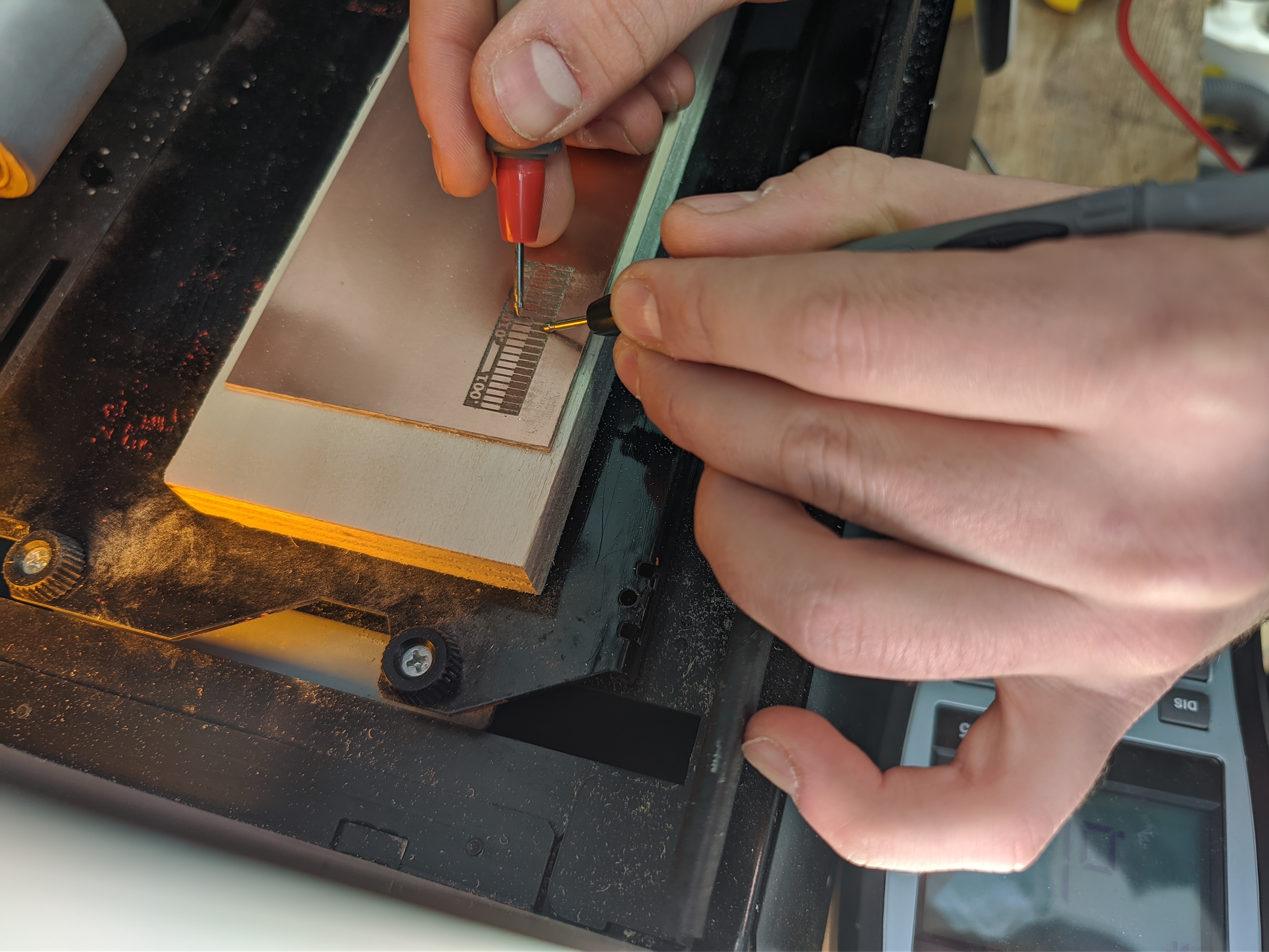
At first, lets practice on the precision test file

present images are in original resolution
To generate path for Roland I use Mods
▼ right click on the empty field
▼ choose programs ▷ open server program
▼ choose PCB png in Roland mill .. SRM-20
▼ add save module and connect it to the Roland SRM-20 millng machine module
▼ change all x y z in Roland SRM-20 milling module to 0
this parameters shifting starting point by defined values
▼ set speed to 3 mm/s
▼ select png file in read png module
▼ look for set PCB defaults module
▼ select mill traces
▼ adjust tool diameter to 0.4 mm
use
mill raster 2Dto convert between mm and inch
▼ adjust max depth to desired value
this value have to correspond the thickness of removed material
▼ adjust cut depth to the same value
this parameter defines depth of single milling pass
▼ set the offset number
this determines if non traces area would be removed
▼ press calulate inside mill raster 2D module and wait to finish
⬤ Traces .rml file is saved to default location
Cutout path
Now let’s proceed with outline cutout

◔ repeat steps from Traces path
▽ replace test.png to test_cutout.png
▽ select mill outline instead mill traces
▼ adjust max depth to the thickness of plate adding ~0.2mm
this would allow cutting through plate and little into sacrificial material to be certain that it cuts ▼ adjust
tool diamererto0.8mm
▼ adjust cut depth to ~0.5mm
this means that if
max depthis2mm machine would cutmax depth, which is little bigger than material thickness, in2 / 0.5 = 4passes
▼ press calculate and wait until end
⬤ Outline .rml file is saved to default location
Milling
Traces
For traces I’m using 0.4 mm end mill that is easy to adjust and doesn’t require any calculations in opposite to V-bit, but more fragile and less durable.
▼ connect Roland SRM-20 and open VPanel
▼ using position controls place the milling head to acess it easily
▼ install the 0.4 collect and the bit and tigthen them loosely
the bit should stick out from collect for 1/3 of it’s length
▼ close the cover and reposition head X/Y to the bottom left plate corner
head position should correspond to desired starting point on the surface but should not exit plate boundaries
▼ descend head with bit until bit tip is almost touching the surface ▼ loosen the bit and place bit’s tip on the surface ▼ tighten a bit well ▼ go to VPanel and set the X/Y and Z origin
look for number 9 in Software section’s control panel picture and find the buttons
X/YZ
▼ press Cut and delete all current jobs ▼ select name.rml file and press Output ⬤ The process have started
you can pause it or cancel using Pause and Cancel
◉ While miling pause and view to examine the piece
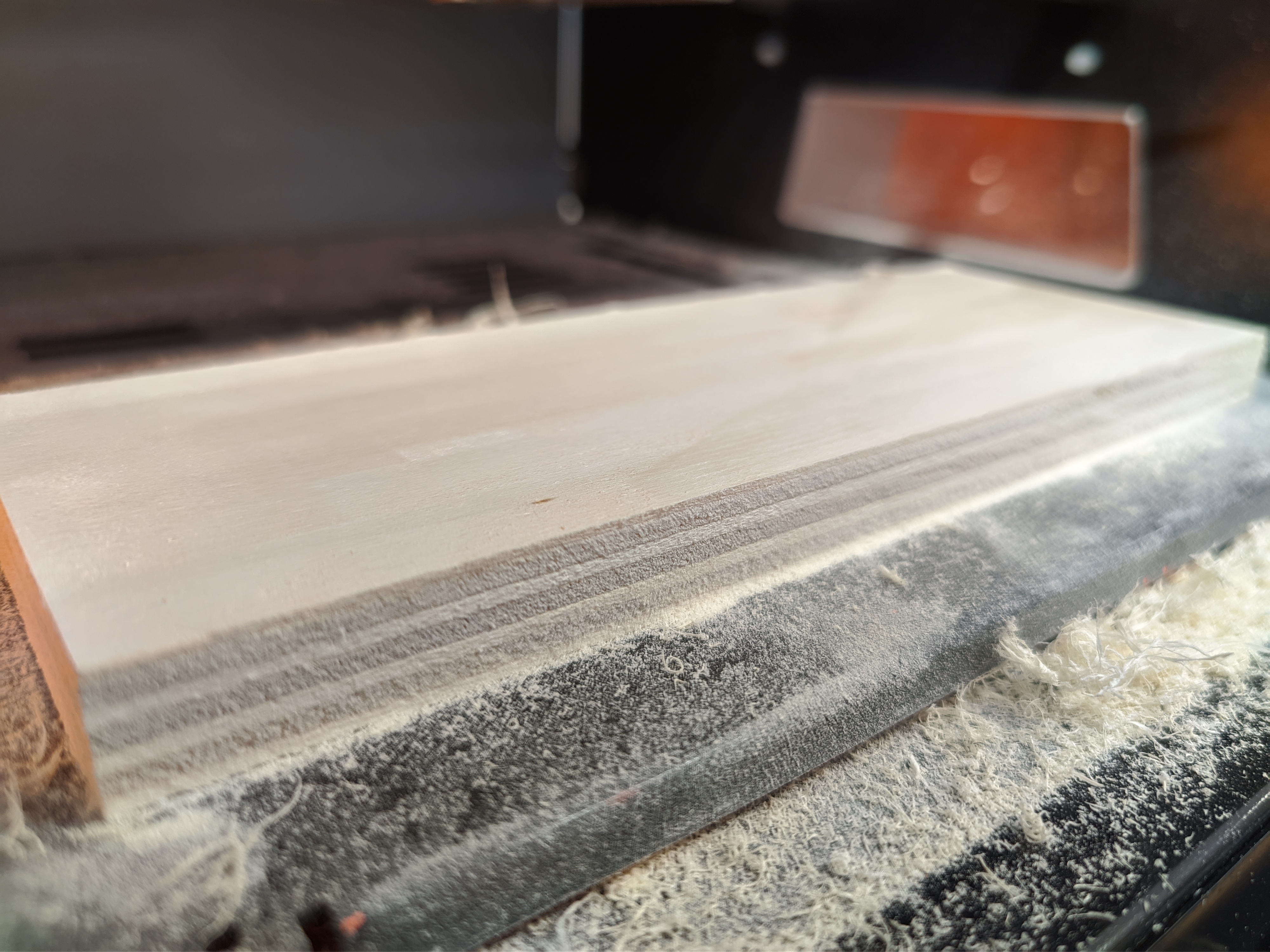
▼ as the process ends remove the dust ▼ check traces isolation
Cutout
Let’s proceed to cutout
◔ Repeat steps from Traces section
▽ replace the 0.4 bit to 0.8 mm
◪ stop at the point where the bit is needed to be tightened well
▼ Make shure that bit’s tip is reaching desired depth
To achieve this move bitless head to the lowest possible position, then move it up for
max depthdistance. Now install the bit and gently place it on the surface. Set new Z origin. Avoid changing X/Y origin otherwise cutout would not fit around traces.
◔ Repeat steps from Traces section starting the process ⬤ The proces is running now
◉ While miling pause and view to examine the piece
▼ remove dust and examine the piece
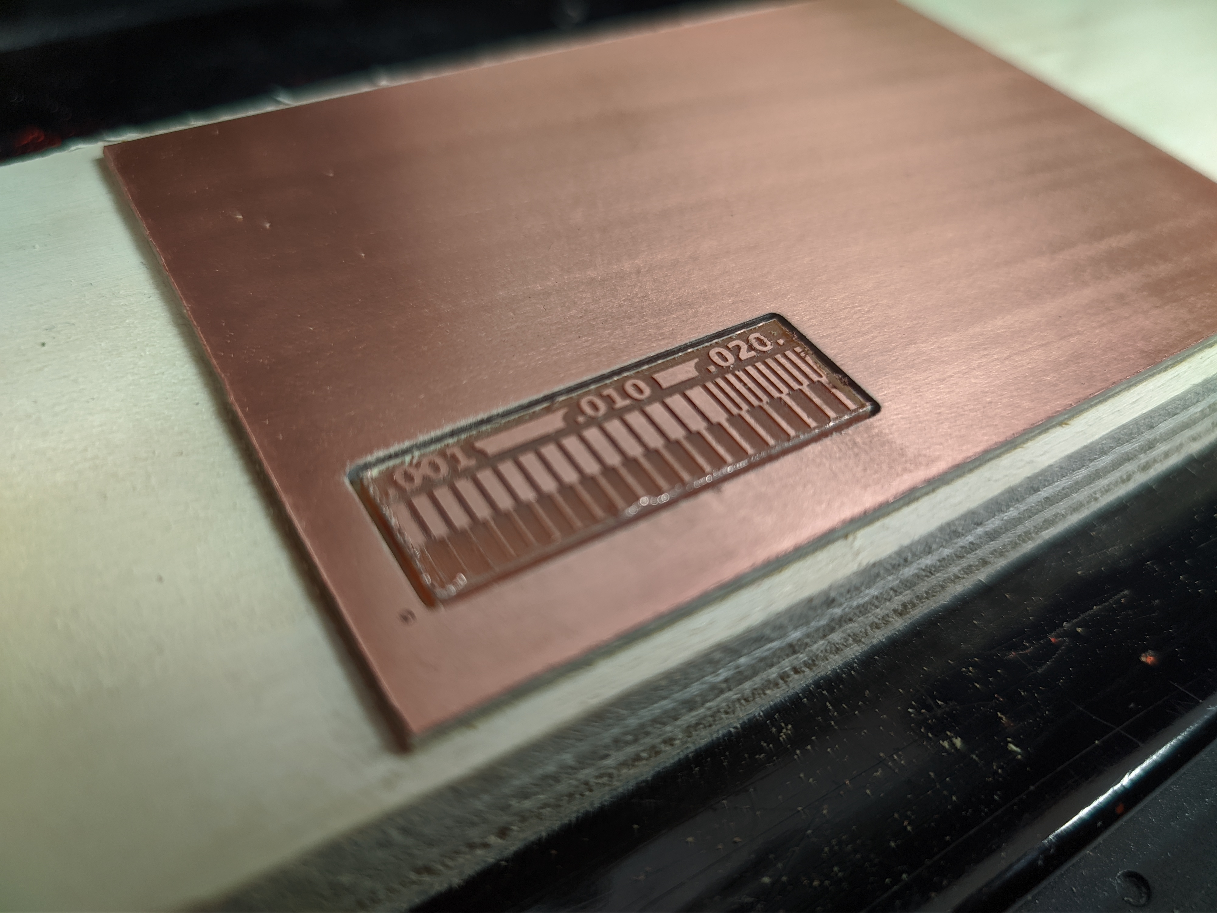 ⬤ The precision test piece is ready now
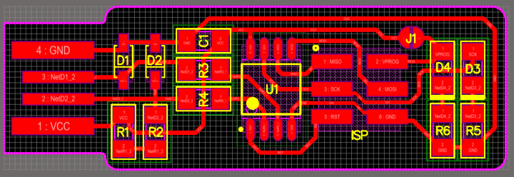
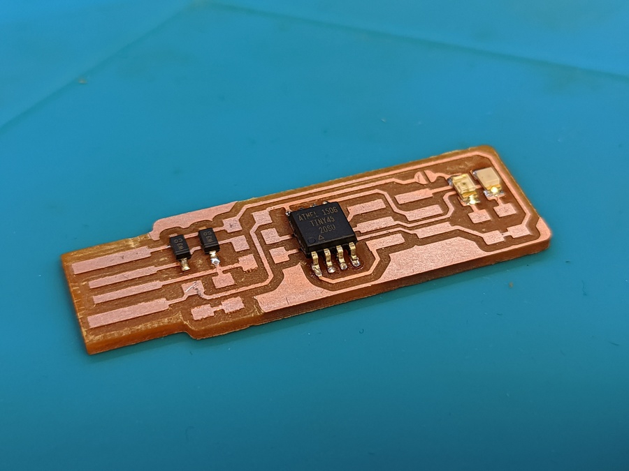
FabTinyISP
Traces & cutout
◔ Repeat Cutting test section adjusting values and replacing .png files
Milling
◔ Repeat Cutting test sequence 👁 cutting the traces
👁 monitoring the process
👁 cutting out the traces
👁 pausing and examining
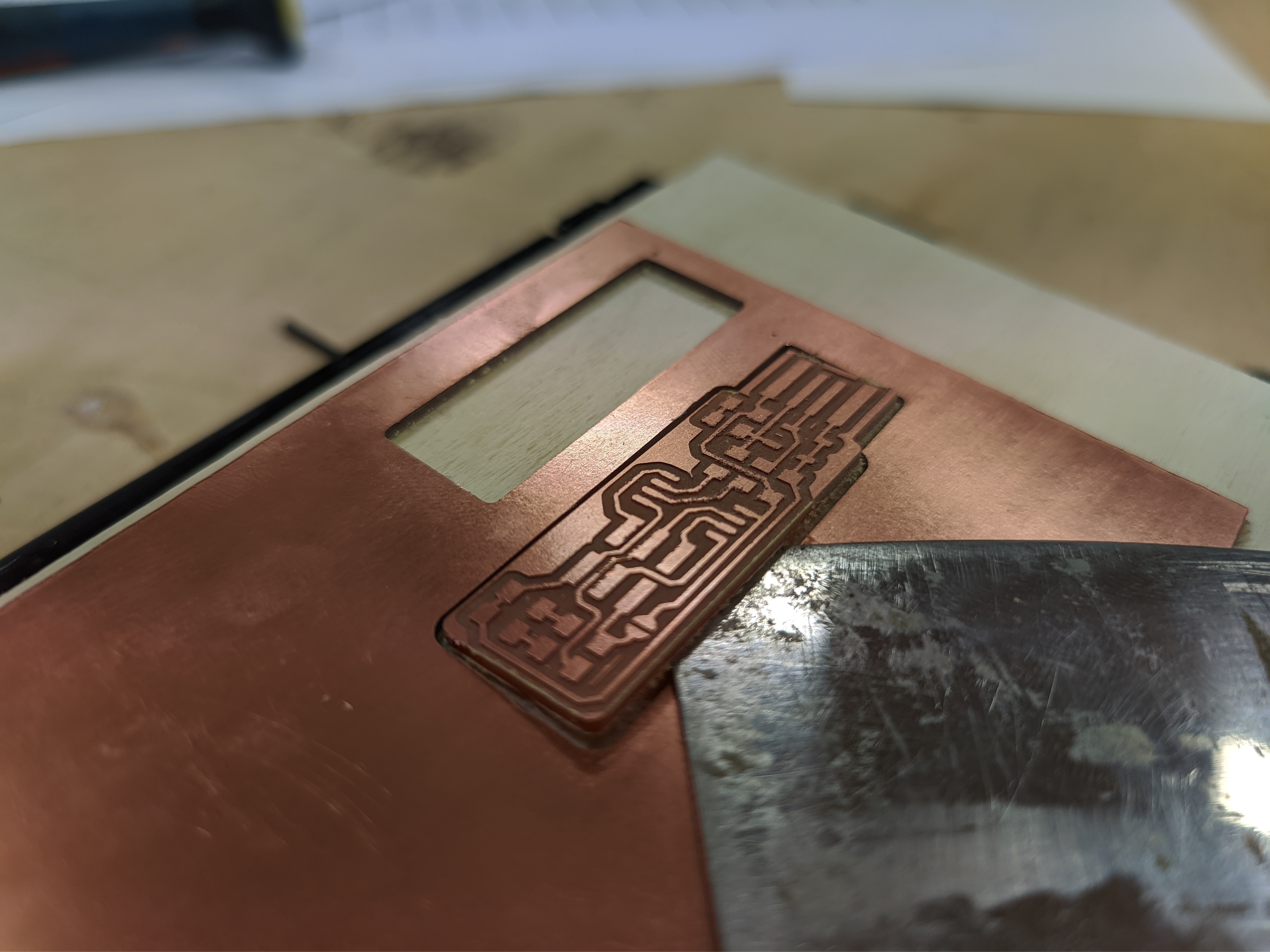
👁 cutting out the board
👁 extracting the board
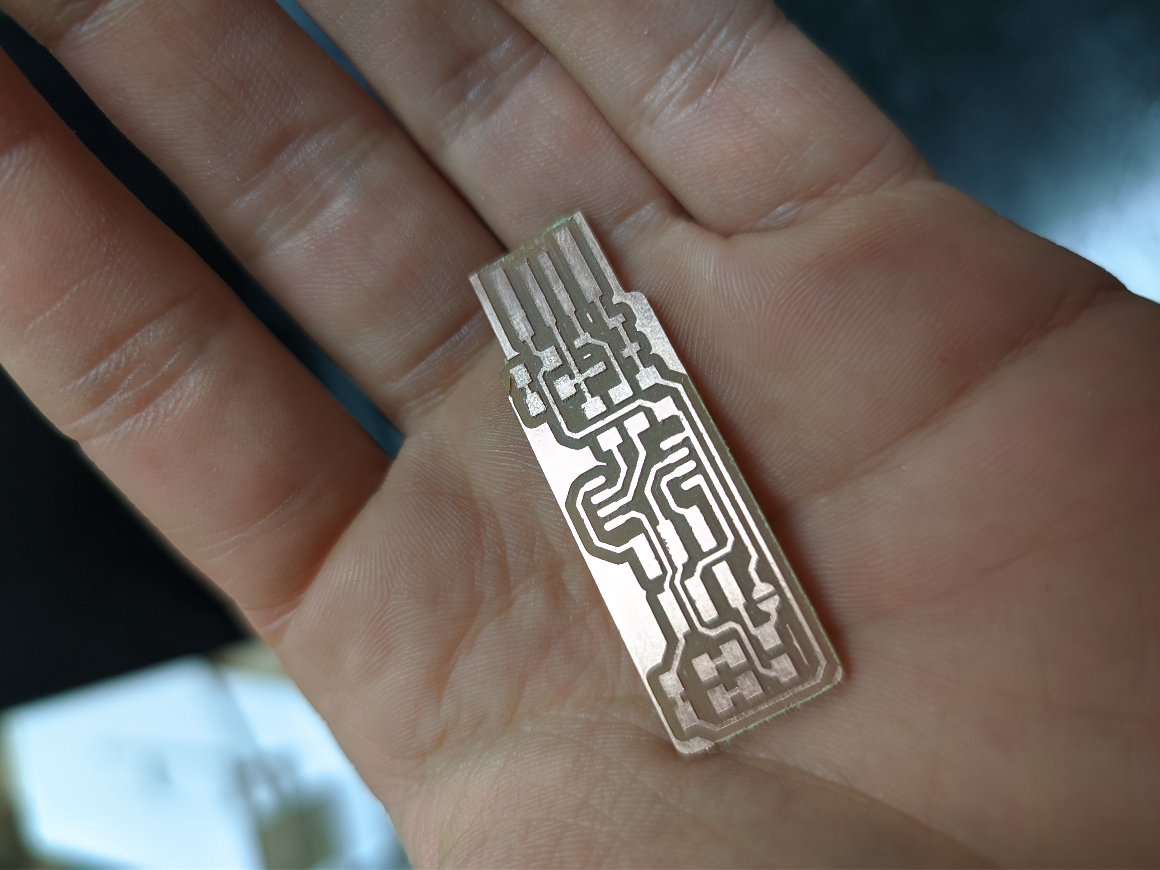
👁 holding the result
Soldering
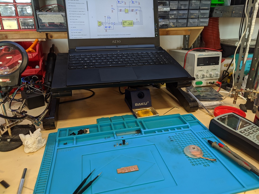
From this point everything is ready for soldering. The last thing to do, but not the least, is to prepare the workspace.
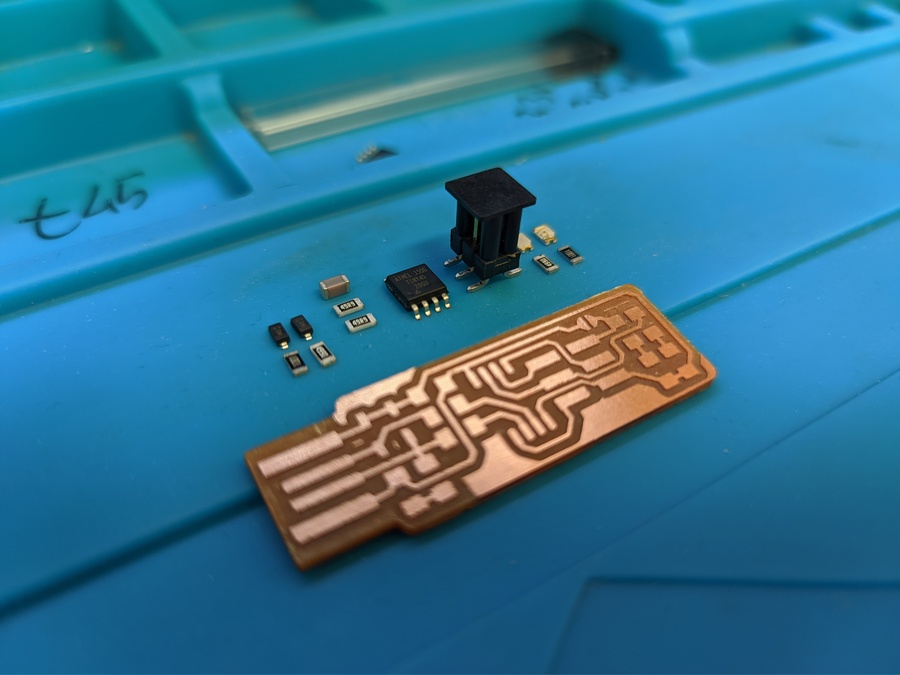
Gather the components
Here is the list of needed components
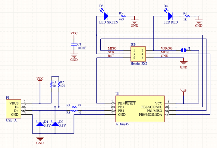
◆ 1x ATtiny45 (or ATtiny85) ◆ 2x 1kΩ resistors ◆ 2x 499Ω resistors ◆ 2x 49Ω resistors ◆ 2x 3.3v zener diodes ◆ 1x red LED ◆ 1x green LED ◆ 1x 100nF capacitor ◆ 1x 2x3 pin header
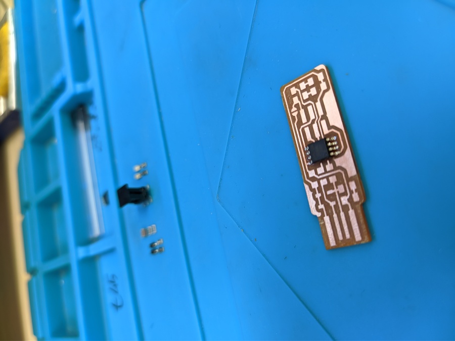
▼ Collect all the components
▼ clean the surface from fat and other unwanted substances
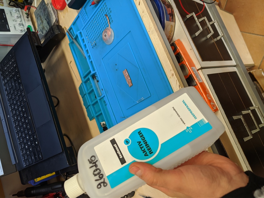
I’m using isopropyl alcohol to remove unwanted substances
▼ place all the components in ordered way
here I’m placing everything on the table in the same positions they should be soldered on the board. I’m doing this just for clarity and to train manipulating with tweezers.
▼ put electronics scheme before eyes to recheck if needed
 ▼
▼
 ▼
▼
ATtiny 45
Start from the hardest parts and from those that have orientation, from center and out
▼ heat up an iron and take a tin wire ▼ preheat one corner leg’s pad with iron ▼ place tin-wire tip on the pad
I’m not using flux for this board because it corrodes copper, but it’s harder for tin to snap on the copper surface. In this scenario it’s better to target copper pad with tin wire rather than iron.
▼ carefully move the wire to the iron until it touches
▼ wait tin to flow
▼ release the wire
▼ spread the tin around the pad surface with an iron
▼ release the iron
◔ Repeat for each ATtiny’s leg pad
For this method, all pads must be covered with thin layer of tin. I’s not easy to glue and align the component when all pads have different amount of tin and if its thickness is too high, because hard blobs of tin would interfere with legs preventing proper alignment.
▼ Take ATtiny with tweezers and place it according to the scheme ▼ align all legs and pads ▼ heat the leg that is on top of the corner pad with iron ▼ wait tin to re-flow ▼ slightly push aligning the component ▼ release the iron ▼ wait until sticks ▼ release the component ◉ Component is glued to the board
▼ heat ▷ re-flow and stick diagonal leg ◔ Repeat the process for each leg adding some tin if necessary ⬤ The MCU is soldered to the board now
Polar components
Now solder other components that have orientation property
⏄ 2 zener diodes ⏄ 1 green diode ⏄ 1 red diode
Component orientation can be determined checking marks on them or using multimeter. When the multimeter is detecting voltage the orientation is correct, and the cathode (thicker line on the markings) is on the black (negative) probe.
▼ glue the component ▼ apply tin to the opposite side of the component ▼ add tin to the first side and ensure it holds ◔ Repeat for each diode
▼ check diodes and traces with multimeter
Multimeter should read power flow in one way but not in reverse. In reverse, it reads for a fraction of a second and then stops.
 ⬤ Orientation sensitive components are in place now
Resistors and capacitor
The rest components can be placed in any direction, so I preferred to install them last
◔ Repeat the process as for Polar components sequence ◔ Install the pin header using ATtiny section steps
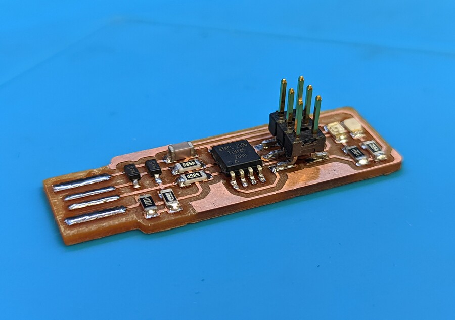
▼ create a tin bridge on the jumper near the ISP header (J1) ⬤ The FabTinyStar is assembled and ready for flashing now
Flashing
Before installing the software, be sure that:
◆ All the components are in place according to schematics ◆ Solder connections should be smooth and stick to the pad as to the pin ◆ Solder should be localized strictly around pad surface area ◆ Multimeter must not read any current the VCC and GND
The software
The flashing process is different depending on the OS. I’m using Windows with WSL in my work-flow. Flashing process on Linux is much easier, but WSL doesn’t fully support USB devices. Though you can use Windows for flashing, installing Linux in dual boot might be even simpler. So, that is what I did. Even on the fresh system no additional configuration is needed. Just run some commands and done!
▼ run
sudo apt-get install avrdude gcc-avr avr-libc make
◉ Linux is ready for flashing
Firmware
▼ Download the firmware Download
▼ unzip and go to the source directory
There are more than one folder in it.
▼ right-click on the empty folder field and open terminal
▼ run make command
👁 now fts_firmware.hex file should appear
▼ run nano Makefile
▼ look for PROGRAMMER ?= usbtiny line
▼ replace usbtiny to programmer name of choice
In my case it’s
avrisp2.
Connection
The precaution measures must be applied to reduce the risks
◆ Use extension cable to remove the strain on board and USB port
▼ connect the programmer and the board to Linux 👁 The red diode on the board should lit-up now
▼ connect programmer to the board
Orientation sensitive! You must align first pin from the board with the first pin on the programmer.
👁 The green light on the programmer should lit-up now
The flashing
Further steps will succeed if everything is done right and all the components are functional
▼ run make flash from firmware folder
◉ The .hex file is written into the ATtiny memory
▼ Disconnect everything from everything
▼ connect the board to Linux machine
▼ run lsusb in terminal
Many things could go wrong, and we need to be sure that board is recognized. For some reason I was not able to discover my unit under Windows system. These issues are listed in FabAcademy’s tutorial, so I decided to install Linux to be sure 100% that piece is working.
👁Multiple Vendors USBtiny should be listed in terminal printout
▼ run make fuses command
⬤ All fuses except the Reset Fuse are set up
Blow the Reset Fuse
Next steps are (almost) not reversible, so be sure that everything is in place and there are no errors encountered during former steps
▼ run rstdisbl
◉ All fuses are now set
▼ Disconnect VCC from Vprog removing the bridge on the solder jumper
⬤ Done! The programmer is programmed now.
Many things could go wrong, but luckily it succeeded. Now I hope I would be able to program something with it!
Links
NOTES: