7. Electronics Design
This week I worked on:
- Learning Electronics
- Learning EAGLE
- Redraw an echo hello-world board
- Adding Components
- Reflection
- Testing the board
- Link to Group Assignment
Learning Electronics
This week I spend the time growing my understanding of electronics. I researched some videos on LinkedInLearning and found several electronic foundation videos:
Some of the videos I found were: 1. Electronics Foundations: Fundamentals by Barron Stone 2. Electronics Foundations: Building Circuits
Breakdown of the videos
In the Electronics Foundations: Fundamentals by Barron Stone, I learned about electricity and how it works. The main take away I got from this course is that, at the end of the day, when working with electronics, I’m just moving a bunch of electrons around using voltages to push them and circuits components to lead them where they need to be. This course was estimated to be 1 hour and 17 minutes.
In the Electronics Foundations: Building Circuits, I learned about designing and assembling electronic circuits. The course was meant to give me the know how’s and the understanding of how circuitry works in order to work with existing ones or design my own.
Learning EAGLE
EAGLE (Easily Applicable Graphical Layout Editor) is a flexible and expandable EDA schematic capture, PCB layout, autorouter and CAM program. To download and install EAGLE, I went to AutoDesk. The installation was quite simple and sooner or later, I was up and running with the application.
To learn EAGLE, I followed a LinkedInLearning course about PCB Design with EAGLE. The course was called Learning PCB Design with EAGLE with Taylor Hokanson. This course is approximately 1 hour and 15 minutes.
Additionally, I followed the FabLab tutorial on Week 6: Electronics Design and received help from my instructor Greg Buckland. Both resource provided me the opportunity to quickly get started with PCB Design in EAGLE. It is also worth noting that Greg, my instructor, often does tutorial session and I used a previous tutorial for guidance on this week assignment.
Redraw an echo hello-world board
To start on the assignment, I opened the EAGLE application.
My PCB design consisted of using the same examples and materials shared on the Fab lab’s Week 6: Electronics Design page. With that said, I build off of the Hello Echo example.
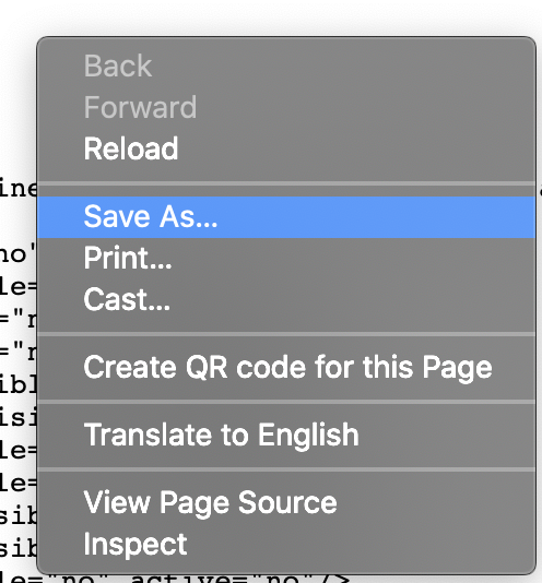
Once I opened the page, I saved the page onto my Desktop by doing “Save As” and leaving the extension to .sch
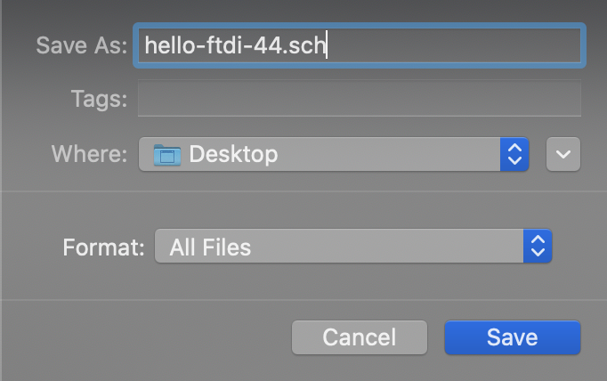
Once the hello-ftdi-44.sch was saved on my computer, I opened EAGLE and created a new project.
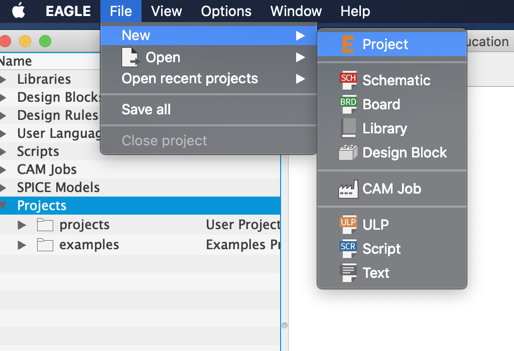
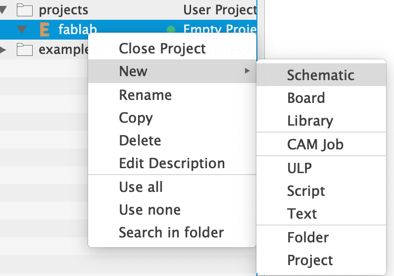
I named my project “fablab.” In fablab, I created a new “Schematic”
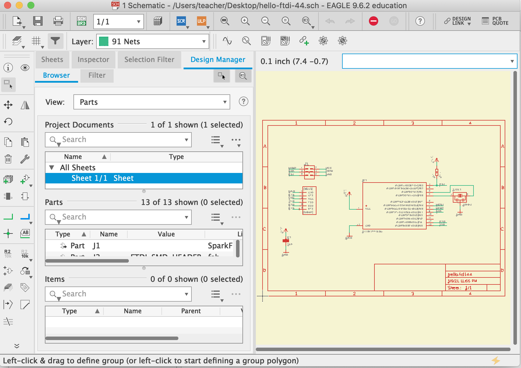
Once I created the new “Schematic,” I opened the Hello Echo in the schematic.
It is worth noting that a schematic, in electronics, is a drawing that represents a circuit by using symbols to represent real-world electronic components. The most basic symbol is a conductor (traces) which is illustrated as a line. If wires connect in a diagram, they are shown with a dot at the intersection.
It is also worth noting that:
- Current => Flow of charge through a conductor
- Voltage => Force that generate the Current
- Resistance => The opposition to Current that is provided by a material, component, or circuit.
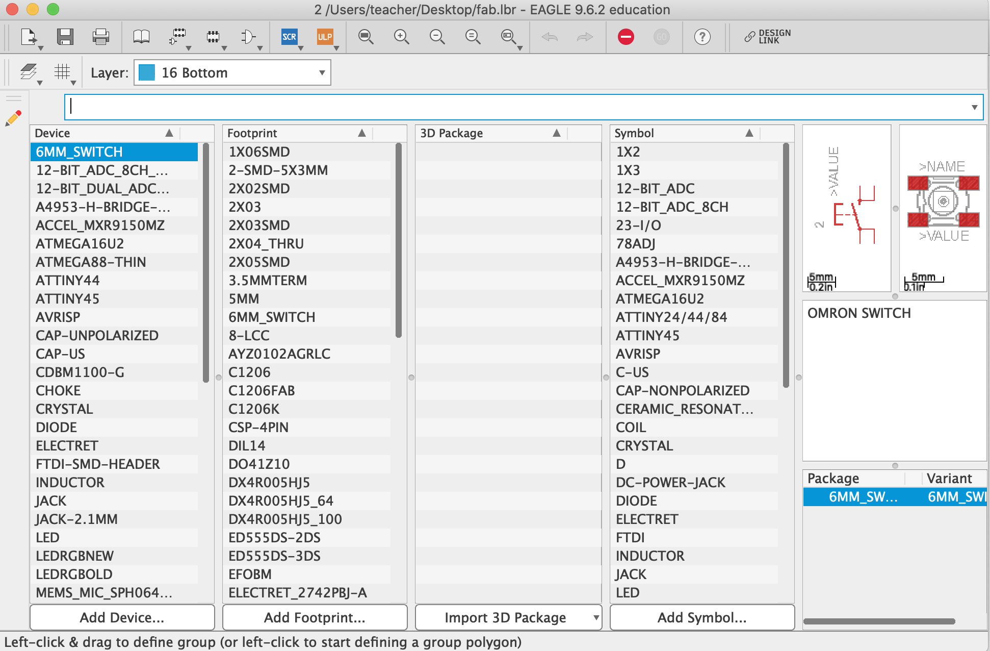
The next step was to add the Fab Lab library to EAGLE’s libraries. The Fablab library can be obtained with this link, FabLab Library
The Fab Lab Library will ensure that I do not get lost in the Eagle’s library. To download the Fab Lab library, I selected “Raw” and took me to a new page with all the raw code. From there, I right-click to “Save As” (Saved as default file - .lbr).
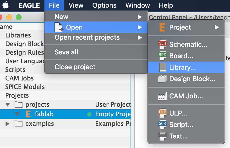
Once the file was saved, I went back to Eagle and selected File > Open > Library:
Now, I have all the Fab Lab components available to me.
Eagle has two windows that you use simultaneously to design a board:
- Schematic (.sch) - logical components
- Board Layout (.brd) for the actual board that we mill
There are 2 ways to interact with Eagle:
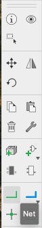
- Graphical Icons Toolbar: You can use the icons in the left-hand toolbar, mouse over them to see what they do. (enabled by default).
- Command Line: You can start typing a command at any point, then select the item in the schematic / board that you wish to interact with, see section on commands below.
If you are interested in using the Command Line, here’s a list of the EAGLE commands: Commands
Being new to EAGLE, I decided to use the Graphical Icons Toolbar
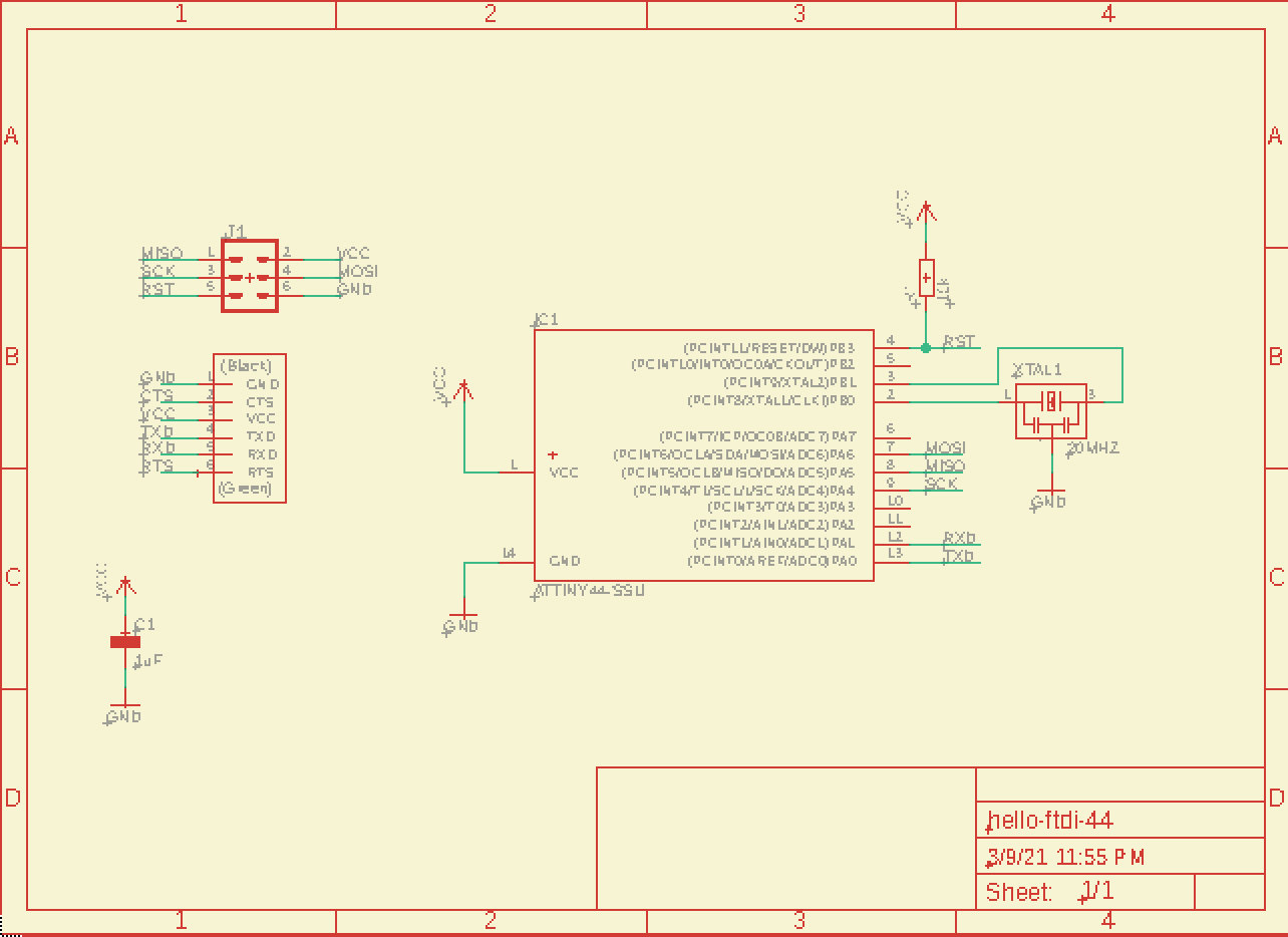
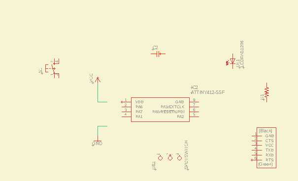
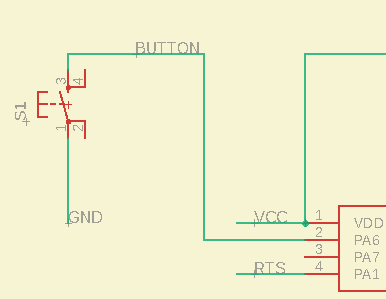
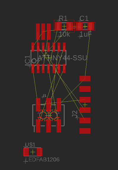
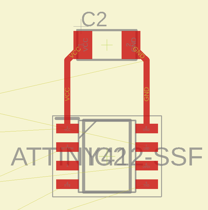
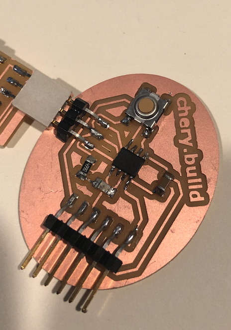
In the Hello Board, below are the parts that were already on the board:
- 6-pin programming header: for programming the board
- microcontroller: attiny44A. Once the microcontroller is programmed, the program stored in non-volatile memory. This means that it will remember the program.
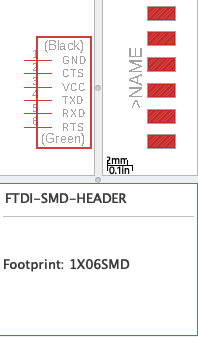
- FTDI header: powers the board and allows board to talk to computer
- 20MHz resonator: external clock. The attiny has a 8Mhz clock but the resonator is faster (increase the clock speed of the processor) and more accurate.
I will be adding the following:
- Resistor
- Button
- Ground
- VCC
- UPDI
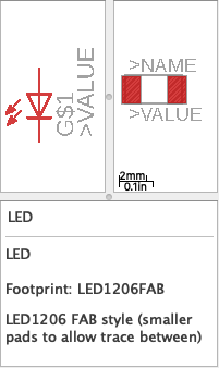
- LED (Light Emitting Diode)
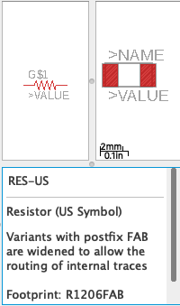
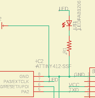
- Resistor (value 499 ohms) Purpose: current limiting resistor
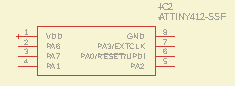
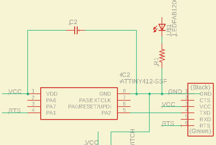
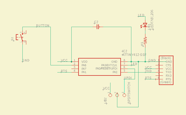
Side note, it was suggested that I switch out the ATTiny44 for the ATTiny412. The ATTiny412 is more relevant and has a better support for components. That said, I replaced the ATTiny 44 schmatic with the Attiny412
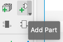
Originally, the Attiny412 was not in the Fab library nor the EAGLE library. So, I installed if by selecting Add Part > Open Library Manager*:
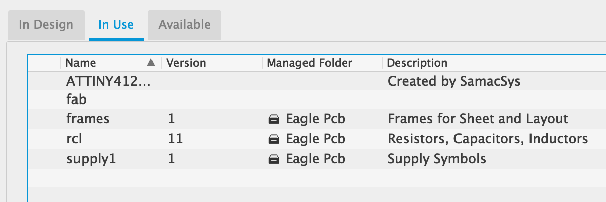
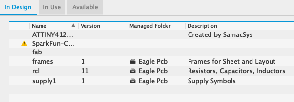
This opened a panel where I had the ability to remove Libraries. I removed the Libraries that I will not be using for this week and added the Attiny412 library. The result was:
To add a library, you select In Use > Browser ** and open the library that you want to use.
So, now, I need to remove the Attiny44 with the Attiny412 and reconnect the connections to the components, the VCC, and the Ground (GND).
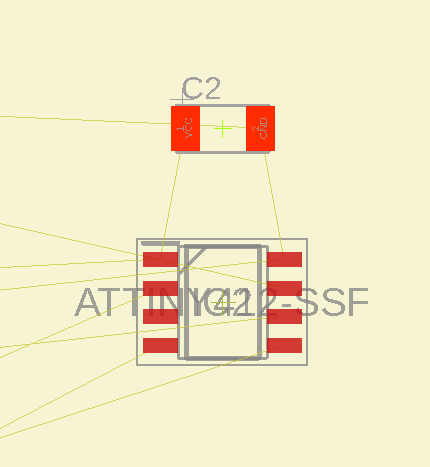
Adding Components
To add a component, select “Add Part” from the Toolbar to the left of the application.
I added the following components:
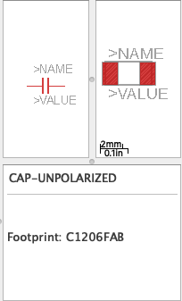
Added CAPACITOR from the fab library:
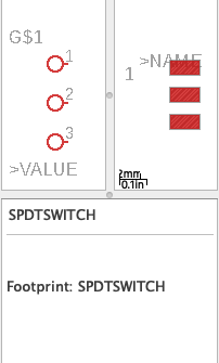
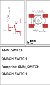
Added SWITCH from the fab library for my UPDI connector:
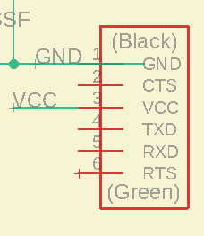
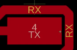
Added FTDI connector from the fab library:
Added BUTTON from the fab library:
Added LED from the fab library:
Added RESISTOR from the fab library:
After I added all the necessary components, I reorganized the components on the schematic.
Connecting The Components:
For connecting my components, I used Net:
The process I used to connect everything were: 1. Starting with GRD 2. Connect all the GRD Up 3. Go to Power (VCC/VDD) 4. Connect all the powers up 5. Different components and work on each of them
In short, the process I did was Ground -> Power -> Components
Connecting GRD:
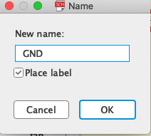
I also wanted to connect the CAPACITOR to Ground (GND). So, I created a Net but, because my schematic started to get cramp, I created the Net to the CAPACITOR on the other side of the page and named the Net GND using:
This allowed me to connect CAPACITOR to ground without having to have the Net go around all the other components.
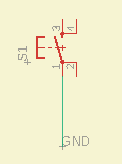
Now, becane I named the Net GND, where the Net is named GND means that those Net are connected electrically.
Connecting Power (VCC/VDD):
Similar to what I’ve done with Ground (GND), I created a short Net from VCC and named the Net VCC:
Now, I have a cleaner/prettier connection
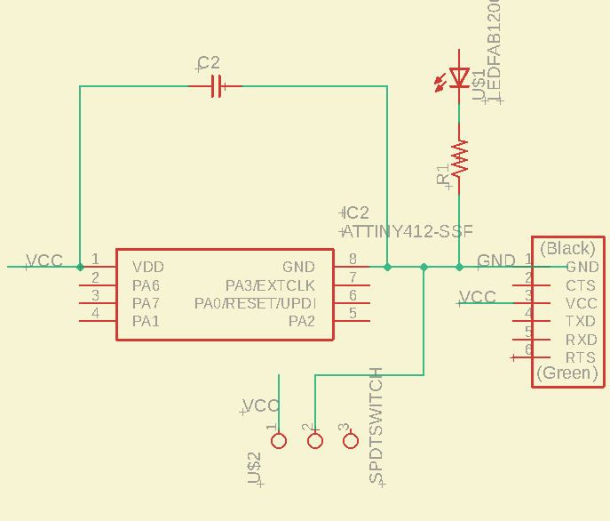
Connecting TXD:
I connected TXD to PA4:
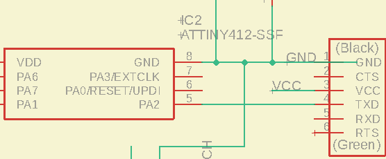
Connecting RTS:
I connected RTS to PA1:
Also, something to note: Dots on the Net means that the lines are electrically connected. No dots, no connection.
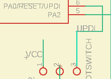
Connecting UPDI Pin:
I moved a Net to make space for the UPDI connection.
Connecting LED:
For the LED, I connected it to the PA3/EXTCLK
Connecting Button:
For the Button, I connected it to the PA6
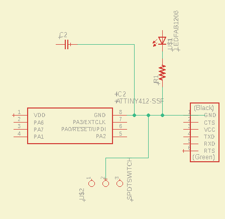
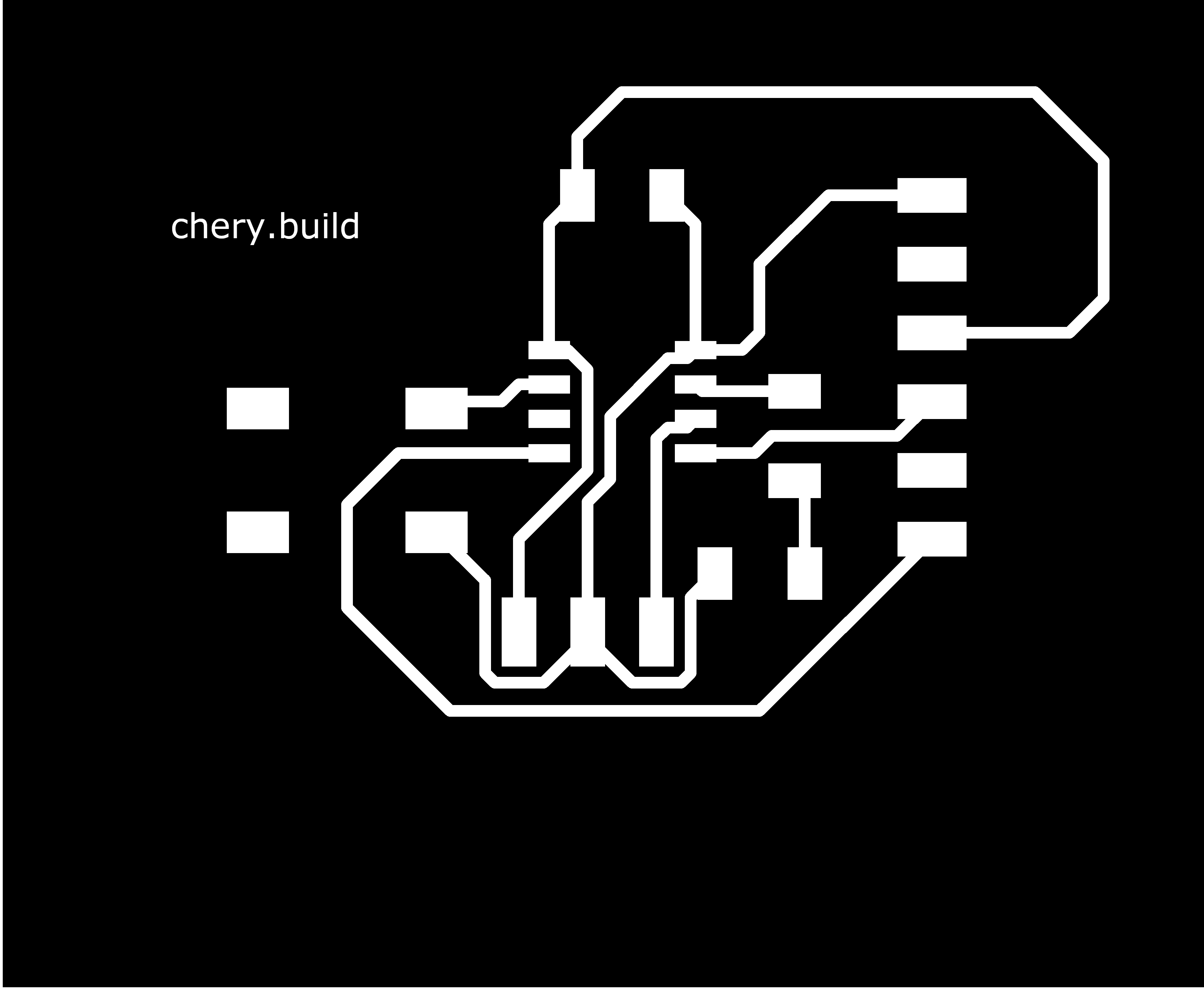
Final result:
Now, the next step is switching to BRD view by selecting:
-
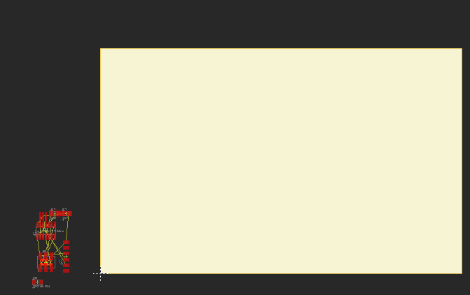
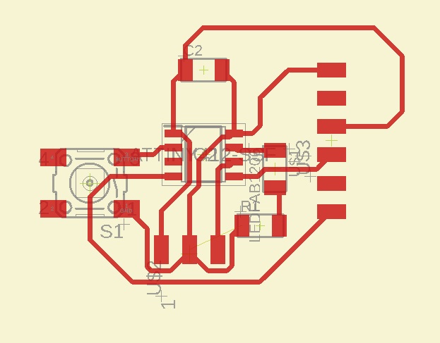
I moved the ATTiny412
-
I moved the Capacitor and routed using the route tool
Route Tool:
With the Route tool, I set the width to 16:

I then routed the Capacitor to the ATTiny412:
- I moved the rest of the components and routed using the route tool:
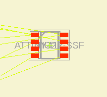
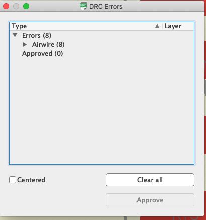
I noticed that the clearances were very small when ti comes to routing. So, I decided to change the Design Rule Check (DRC) found within TOOL > DRC.
DRC (Design Rule Check) => Is the set of rules that is used to check rather or not the board that you design can actually be manufactured.That said, the Fab lab have their own design rule check can can be downloaded here: Link
The result of checking the DRC gave me:
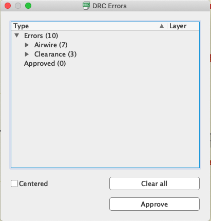
The Airway is okay to have. But, be concerned about the Clearance. The Clearance means that the mill might create an electronic connection between those two circuits.
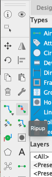
To fix it, select Rip-up:
I ripped up one clearance and the DRC resulted in:
To prep my board for milling, I went to the Layer Setting tool to remove the unnecessary items.

In the layer setting, you can set which layers are visible and which are not visible.
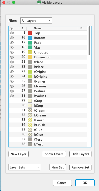
In the setting layer, I worked only the Top layer and made only visible: 1. Top 17. Pads 18: Vias
Finally, I went into File > Export > Image.
For the image setting:
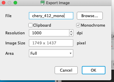
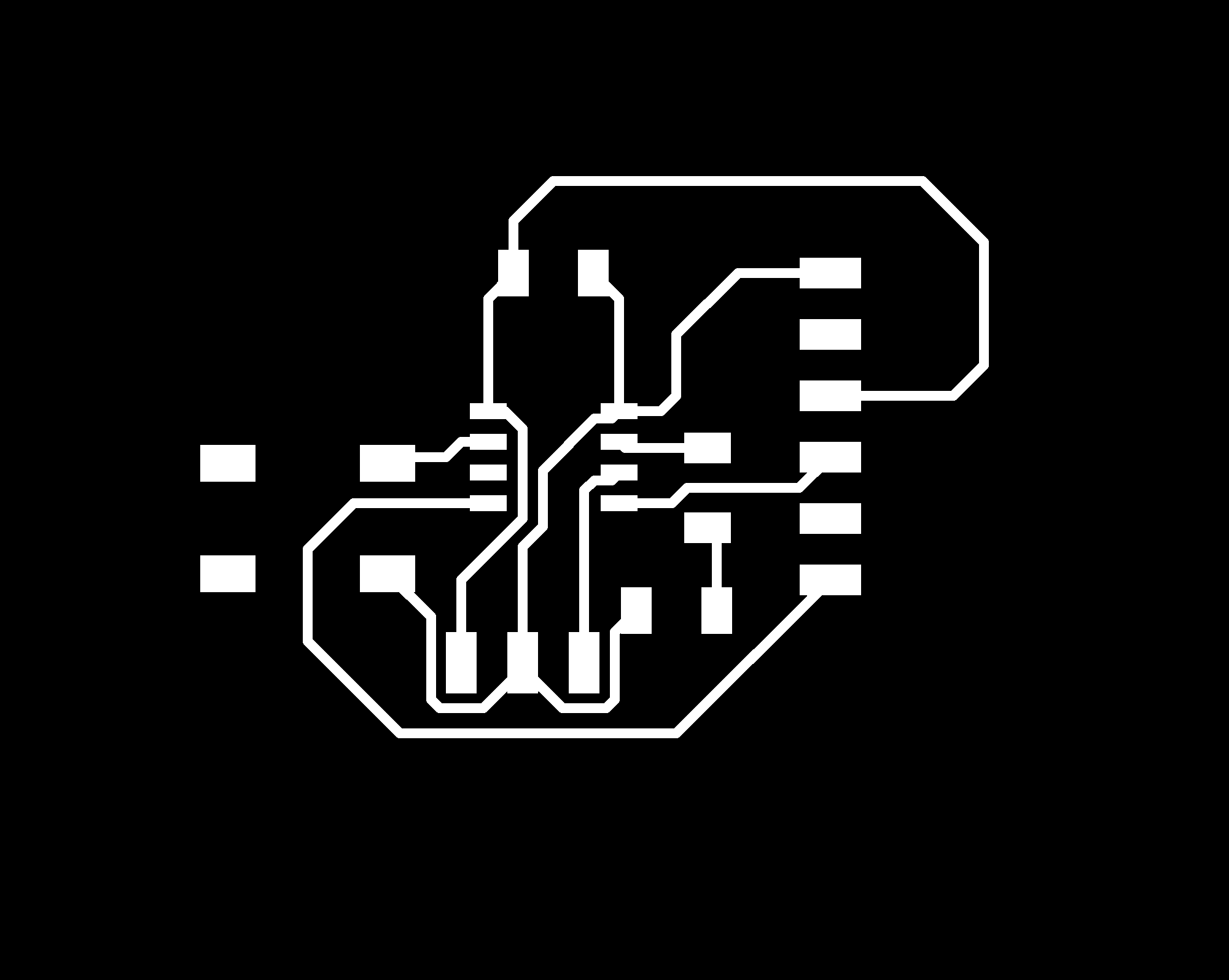
Final outcome:
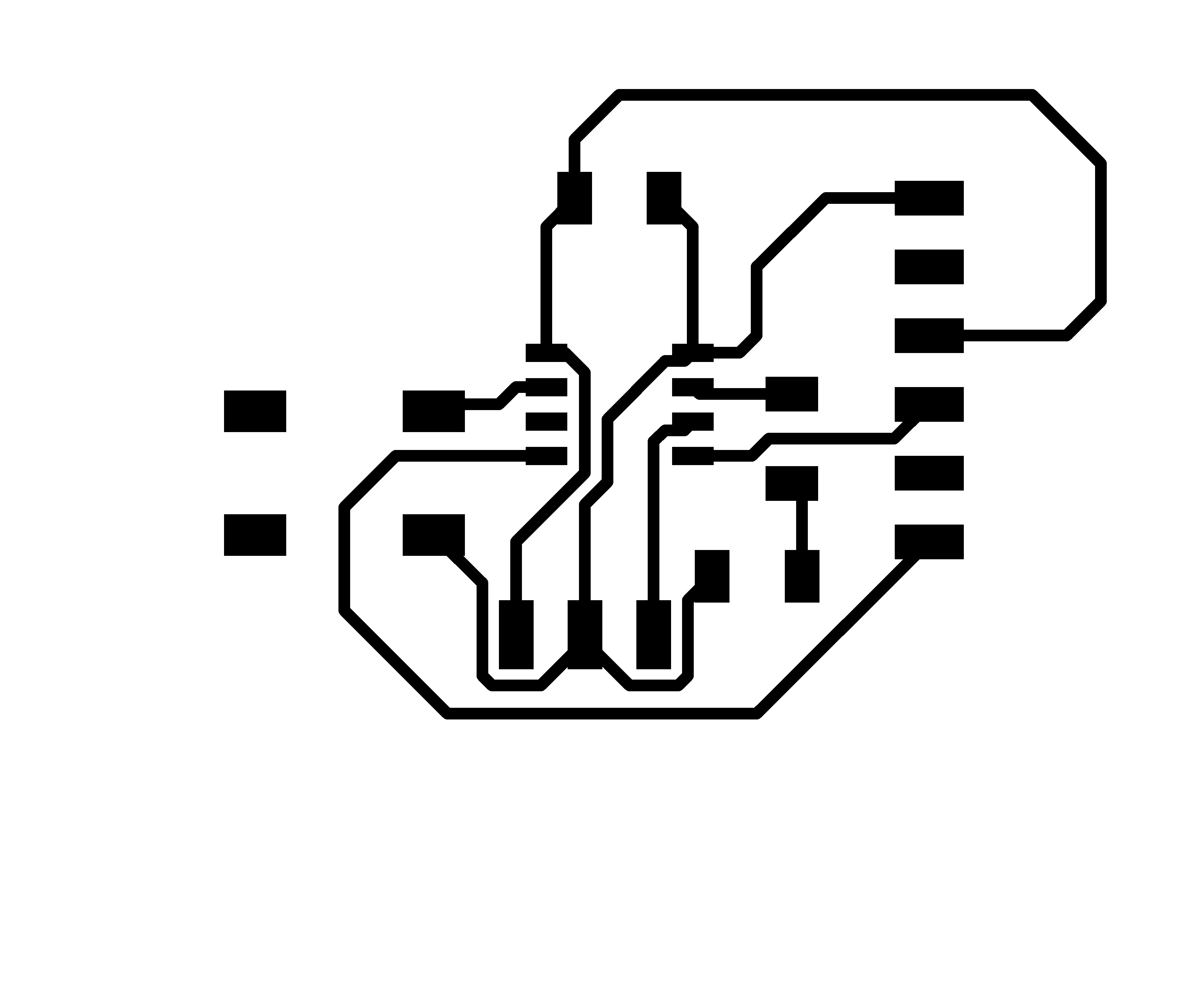
For some reason, the image was inverted. So, I user PineTools to invert the png. The resul was:
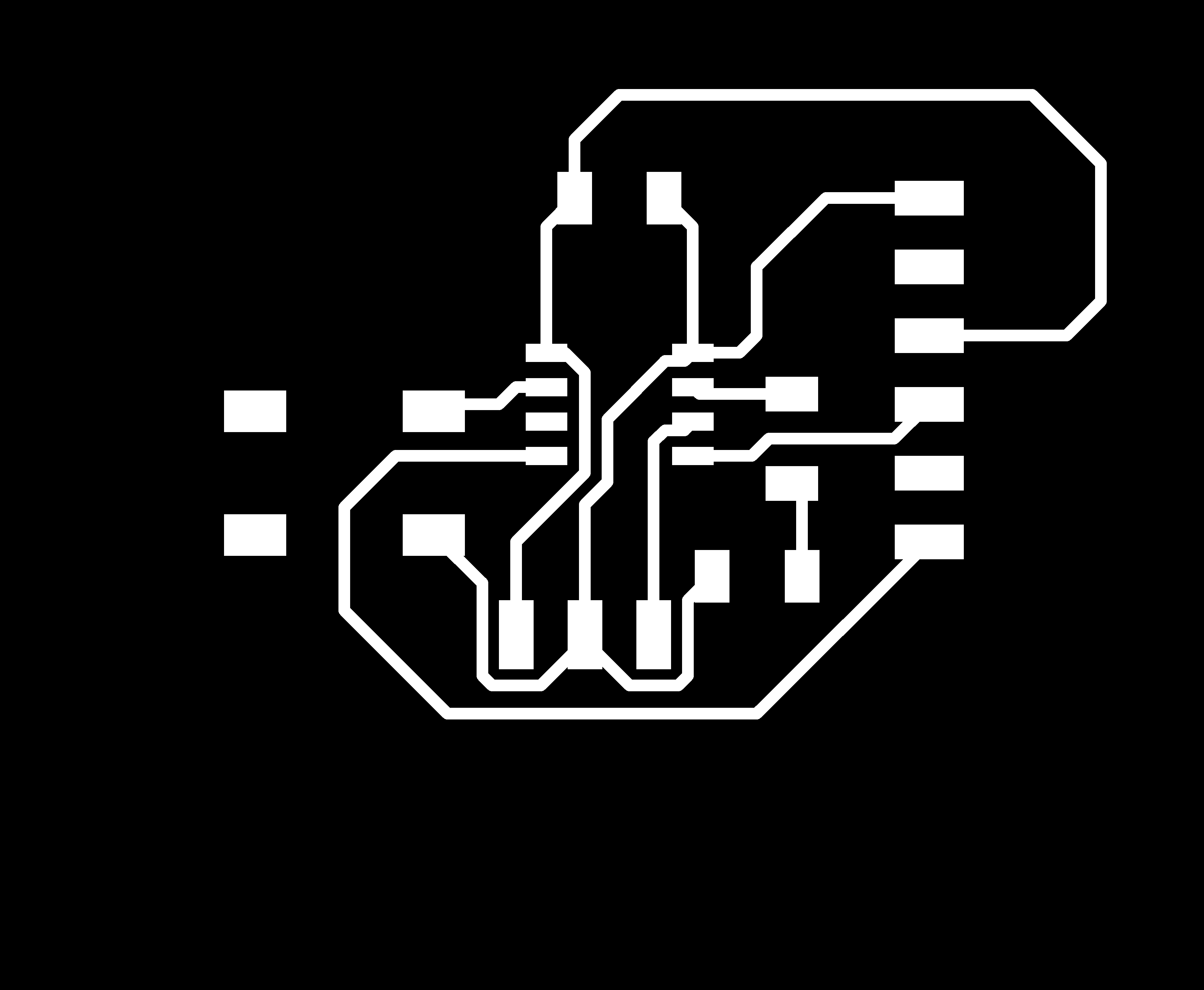
Getting it Ready for Milling To prepare my PCB for milling, I used Gimp.
-
Upload the .png file into Gimp.
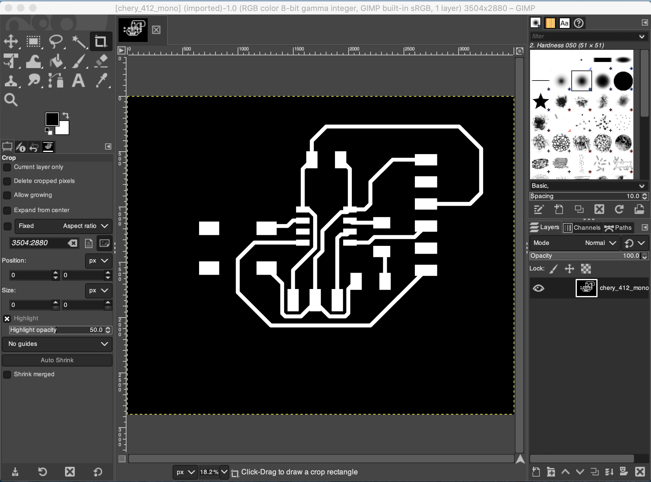
-
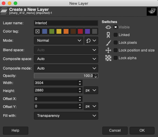
Add a Layer and have the “Fill with:” be Transparency.
-
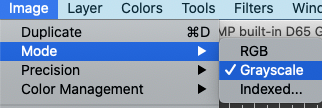
Go to Image > Mode > Grayscale so you can see what’s going on in the background
-
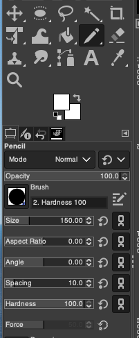
Grab the Pencil Tool and make it a Hard Round Brush and set the size to 150.00
-
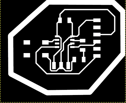
Draw the shape you want to cut out around the PCB’s trace. Make sure you are on the new layer you created
-
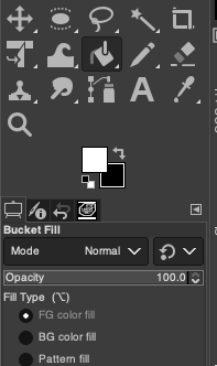
From there, I selected the Bucket Tool to fill in the shape.
-
After doing the above steps, I select File > Export As
Reflection:
I realized that my PCB needed work. That said, I was able to schedule some time with Greg and we was able to help me redesign my PCB. With his help, I was able to create a new design.
Before Greg Help:

After Greg Help:

From there, I went to the lab to print out my PCB:
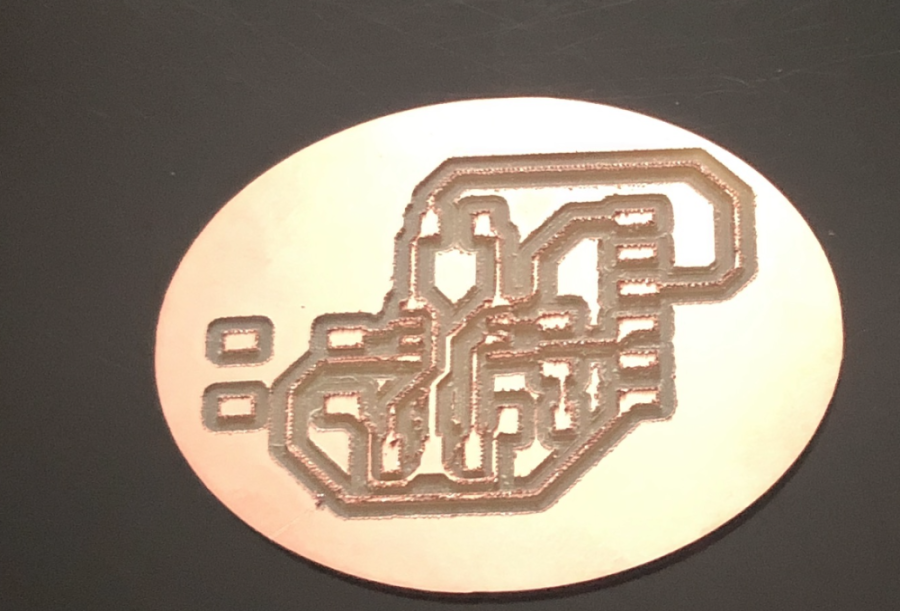
After finishing my electron design, I was able to get some feedback on my design. In the feedback, it was identified that the 1/64 mmill was towrds the end of its functionality. This was identified due to the Traces that came out. I was not confident in the process and decided to redeign the cut and and cut it out. The redeign and the cut of the PCB design can be found in the Week09.
Testing the board
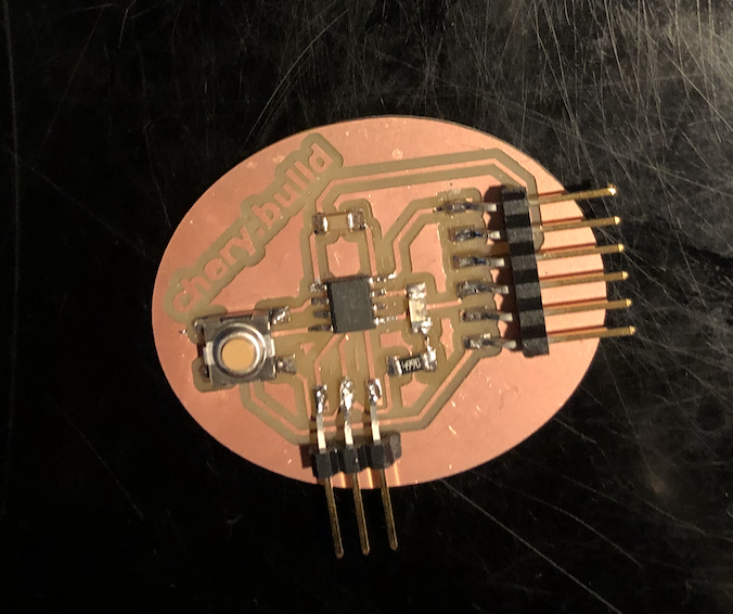
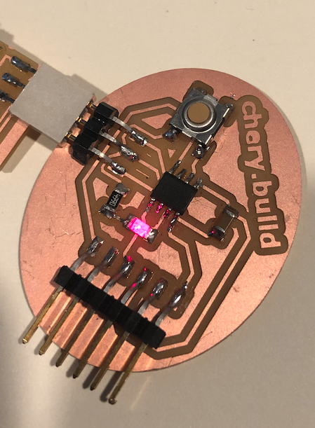
I tested the board by verifying that, when clicking the button, the LED lights up. In order to perform the test, I needed to load some code onto the board.
To get the programming working, I needed a 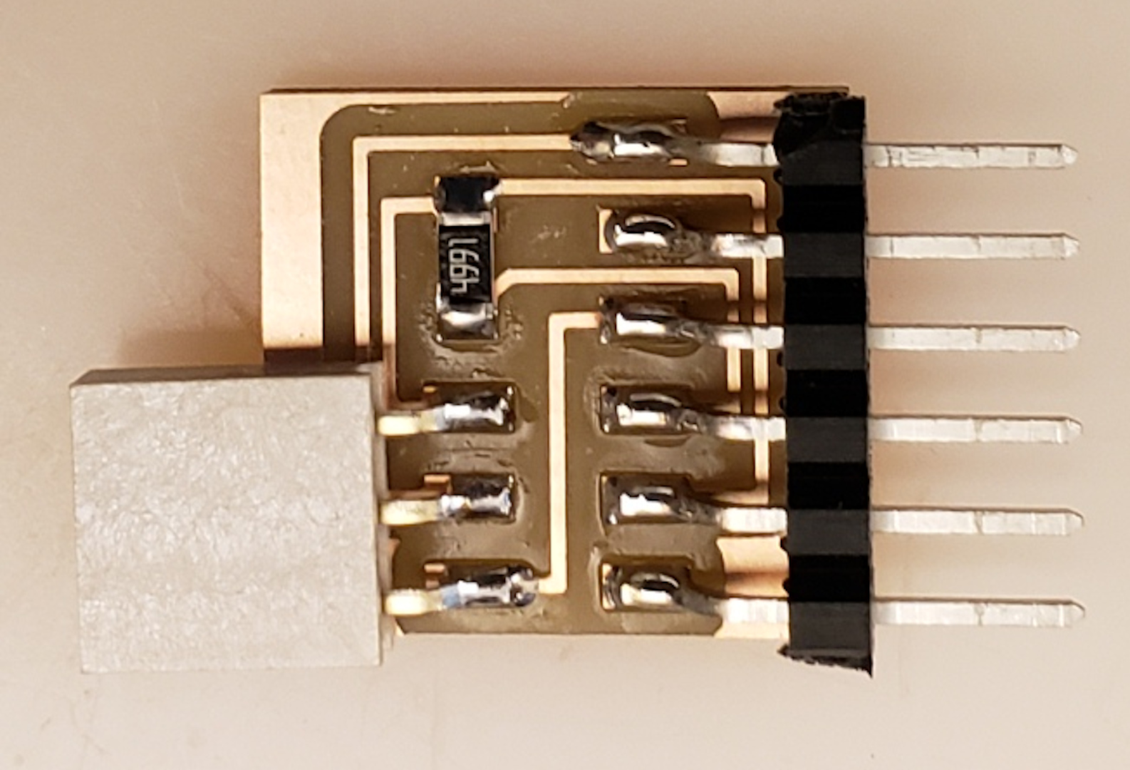 . This adapter was inspired the
 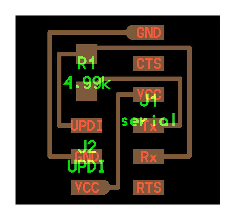 using the following
  and
and  .
.
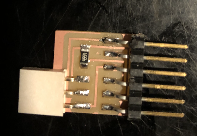
Once I created the adapter, I downloaded the Arduino IDE to begin programming.
To program my board, I needed to first understand how the UPDI adapter, my PCB board, and the FTDI adapter works. I reached out to one of my instructor, Greg Buckland, where he explained the process of embedded programming.
Once I gained an understanding of the process, I was able to test the board by writing a small amount of code that would get the LEF to light up. The results can be shown below:
Link to Group Assignment
This week group assignment was to use the test equipment in our lab to observe the operation of the microcontroller cirvuit board. Group’s Page