6. Electronics design
Week06 will be about Electronics Design. I continue under lockdown (sigh…) and hopeful I can start my run in the Lab early April.
As I’m at home, I’ll invert the assignments again and redraw an hello-world board first and then analyze it with the tools at hand, in this case a multimeter.
Assignments
- Group project:
- use the test equipment in your lab to observe the operation of a microcontroller circuit board
- Individual project:
- redraw an echo hello-world board
- add (at least) a button and LED (with current-limiting resistor)
- check the design rules, make it, and test it
- extra credit: simulate its operation
6.1 (Re) Designing an hello-world board
My first assignment this week was the redesign of an hello-world board, such as this one :)
…and no…I’m not going to do anything fancy or artistic sorry :)
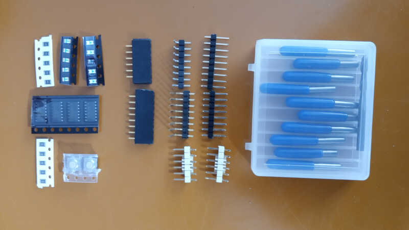
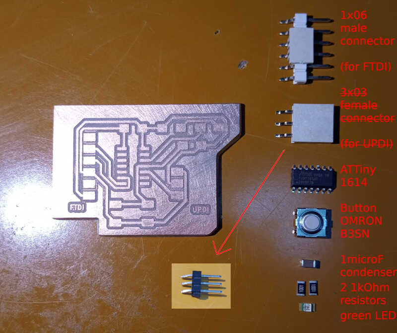
To do this I received from my local instructor André the following components:
- 4 ATTINY1614-SSFR micro controllers
- 2 Tactile push buttons
- 5 SMD Green LEDs
- 5 SMD Blue LEDs
- 5 SMD \(1K \Omega\) Resistors
- 5 SMD \(0 \Omega\) Jumpers (to bridge some traces if needed)
- 2 5x0 Pin Right Angle (for the FTDI connector)
- A few pin connectors to play with
- and some v-bits to be destroyed :P (no, I didn’t scratch the MDF of the milling machine yet!)
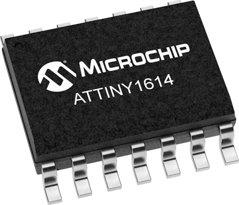
My first step into the world of electronic design was to inspect the mysterious hello world boards everyone talked about during class. I have chosen the ATTINY1614 MC mostly due to their versatility and available arduino libraries.
I quickly went through the ATtinies MC datasheet and no…i didn’t read the 598 pages :)
For a $1 chip it has loads of features. I’ll name here a few that caught my eye. The rest are in the first two pages of the datasheet.
- 20 MhZ AVR CPU (faster than my first PC, a 386SX @ 16 MHZ :O )
- Memories
- 16 KB In-system self-programmable Flash memory
- 256 bytes EEPROM
- 2 KB SRAM
- Write/erase endurance:
- Flash 10,000 cycles
- EEPROM 100,000 cycles
- System
- (excellent) Clock options:
- 16/20 MHz low-power internal RC oscillator
- 32.768 kHz Ultra Low-Power (ULP) internal RC oscillator
- 32.768 kHz external crystal oscillator
- External clock input
- Single-pin Unified Program and Debug Interface (UPDI) - I hope I can use my ftdi board from week04 to program this one through UPDI :)
- (excellent) Clock options:
- (loads and loads of) Peripherals
- One 16-bit Timer/Counter type A (TCA) with a dedicated period register and three compare channels
- Two 16-bit Timer/Counter type B (TCB) with input capture
- One 12-bit Timer/Counter type D (TCD) optimized for control applications
- One 16-bit Real-Time Counter (RTC) running from an external crystal, external clock, or internal RC oscillator
- Watchdog Timer (WDT) with Window mode, with a separate on-chip oscillator
- One USART with fractional baud rate generator, auto-baud, and start-of-frame detection
- One master/slave Serial Peripheral Interface (SPI)
- One Two-Wire Interface (TWI) with dual address match
- Philips I2C compatible
- Standard mode (Sm, 100 kHz)
- Fast mode (Fm, 400 kHz)
- Fast mode plus (Fm+, 1 MHz)
- Three Analog Comparators (AC) with a low propagation delay
- Two 10-bit 115 ksps Analog-to-Digital Converters (ADCs)
- Three 8-bit Digital-to-Analog Converters (DACs) with one external channel
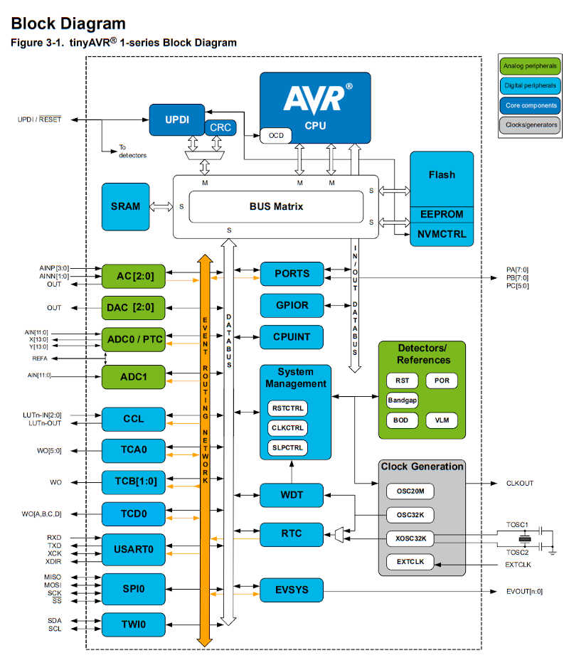
An embedded MC is an impressive device packing lots of powerful stuff. It has many elements of a normal computer packed into a very small package: CPU, volatile/non volatile memory, I/O ports, clock generation…as well as other features, such as signal detectors with references, ADC and DAC…and so on. This can be observed in the Block Diagram of the tinyAVR-1 series.
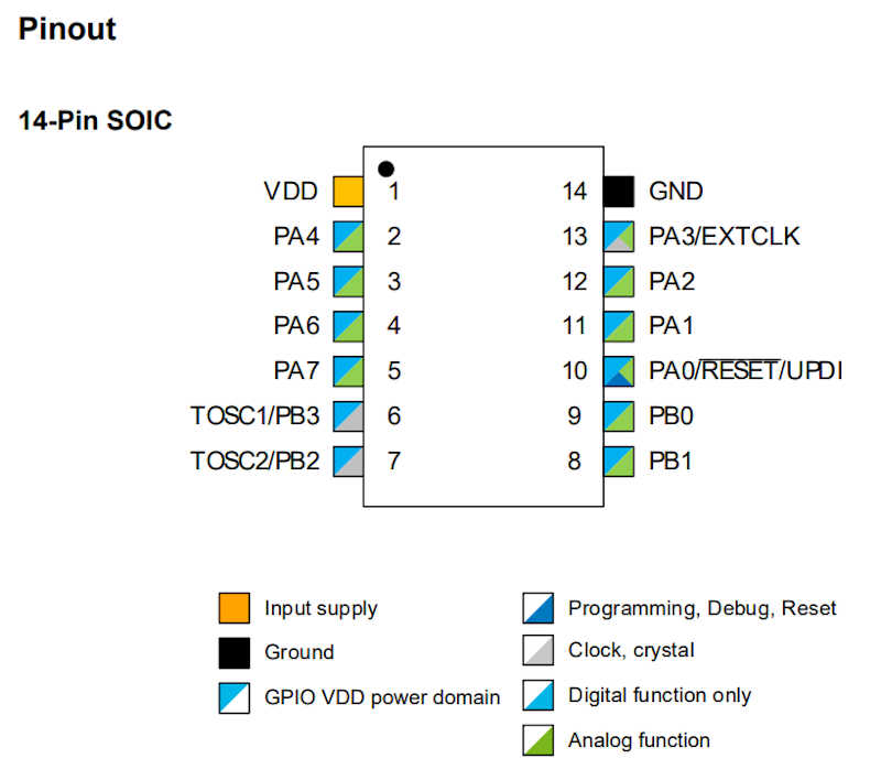
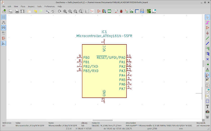
It is very important to check the pinout to know where to plug things. In my case, I have a 14-pin SOIC as shown below.
For now, I’ll leave it at that. I will need to crunch through this datasheet soon enough!
Designing Neil’s ATTiny 1614 Board
The starting point will be Neil’s ATtiny1614 board design. The info is on the Embedded Programming page. Search for ATtiny1614 and you’ll get there. It’s the second reference.
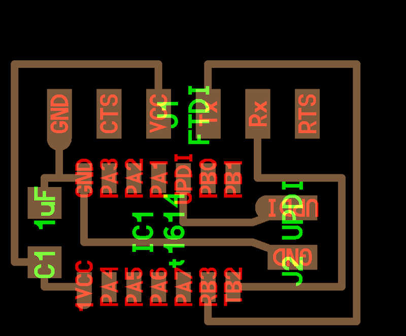
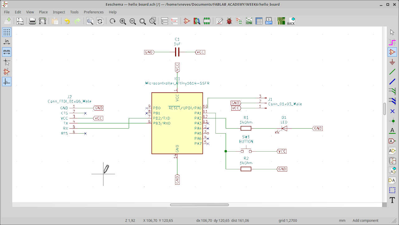
From here I took the Neil’s schematic, shown below, and replicated it in Kicad. Kicad will be the program of choice for electronics design.
Doing some very straightforward reverse engineering, I could replicate the circuit easily. But the idea here is to redraw the board! What will be the best approach? Let me think for a while…
First I created a new project on Kicad and called it hello_board. After creating it, I had two choices: i) to check out the PCB Layout or ii) the PCB schematics. I’ll start by drawing the circuit on the schematics, using the available FAB Footprint and Symbol Libraries.
The Symbols on the one hand are the schematic functional representation of the component, giving important information related to I/O ports and their functions. It is possible to connect symbols with wires in the Schematic Layout Editor. The Footprints on the other hand are the outline of a component that is mounted on a circuit board. It contains the pins, the device and sometimes text markings and values related to the component.
The FAB Libraries were previously cloned from their gitlab repository and installed in a convenient directory. Is it important to regularly update the git using git pull at the lib location.
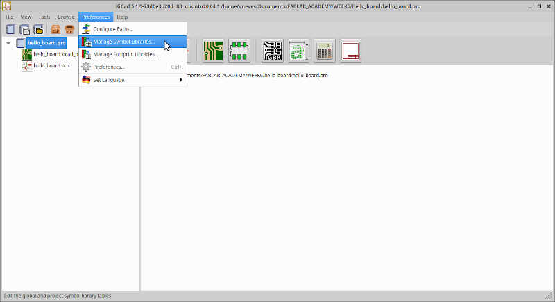
To install the libraries I needed to go to Preferences/Manage Symbol Libraries and Manage Footprint Libraries.
Then,
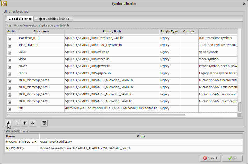
- in
Symbol Libraries/Global LibrariesI clicked on the plus signal on the bottom left corner of the window and addedfabas the nickname of the new library, adding the following Library path:homedir/kicad_lib/kicad/fab.lib.
-
in
Footprint LibrariesI did the same thing, also callingfabto the new library and the following path:/homedir/kicad_lib/kicad/fab.pretty. -
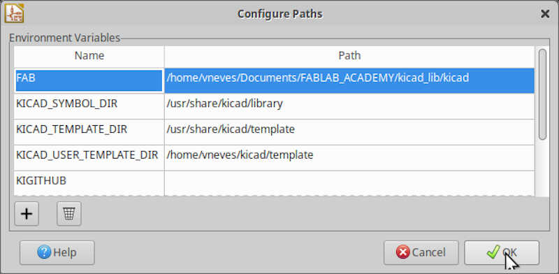
In the
Preferences/Configure Pathsmenu, I added capitalFABfor the environment variables and added the path of the Fab Kicad Libraries:/homedir/kicad_lib/kicad. This way kicad will know where the FAB libraries are located.
After this initial setup I laid out the components from Neil’s hello-board:
- 2x01 Pin array for the UPDI connector - I saw immediately I was going to replace the original 2x01 pin for a three pin version, so that I could feed 5V from my USB to UPDI programmer, done in Week04, to this board. The UPDI will be used to program the 1614.
- 6x01 Pin array for the FTDI connector - I’ll need the FTDI connector to communicate through the serial port with the 1614.
- ATTiny 1614 IC.
- 1 \(\mu F\) Capacitor.
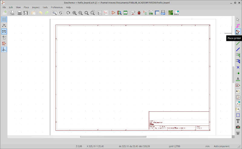
The first thing to place in the Schematic Layout Editor (Tools/Edit Schematic) is the 1614 IC. To do that I clicked on Place Symbol, the third icon on the right
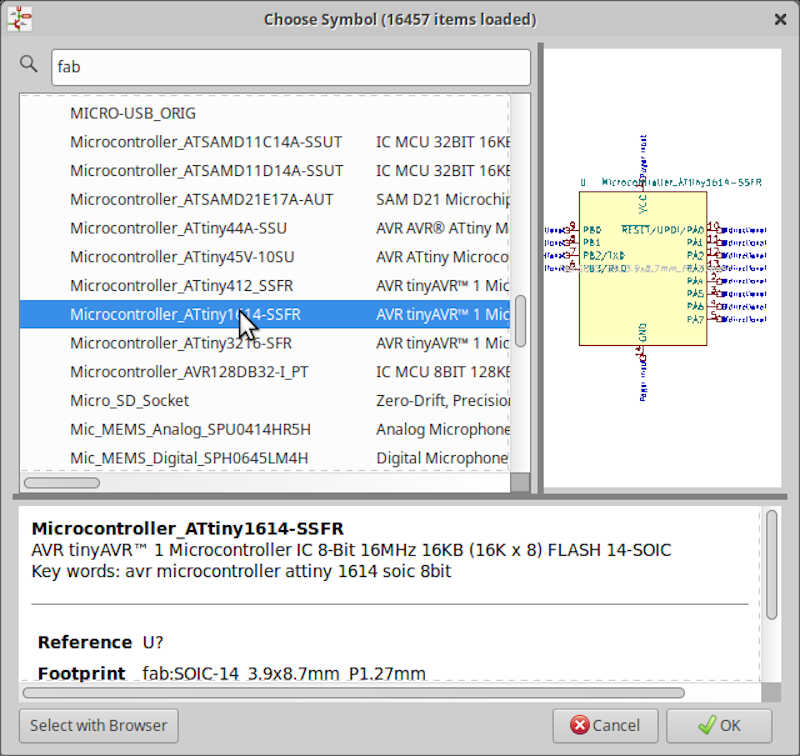
Then, I clicked on the empty schematic and the Choose Symbol window appeared. I wrote fab, to go directly to the fab symbols and chose the ATtiny1614 as shown in the picture.
I placed it at the center of the schematic, deselected the Place Symbol tool with the ESC key, clicked on the label U? and changed it to IC1. You can change the names of other labels in a similar way.
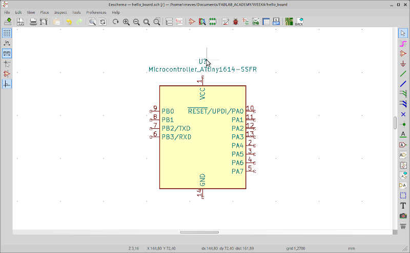
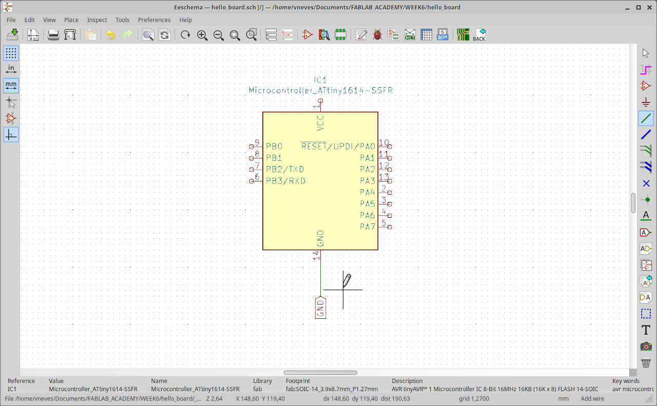
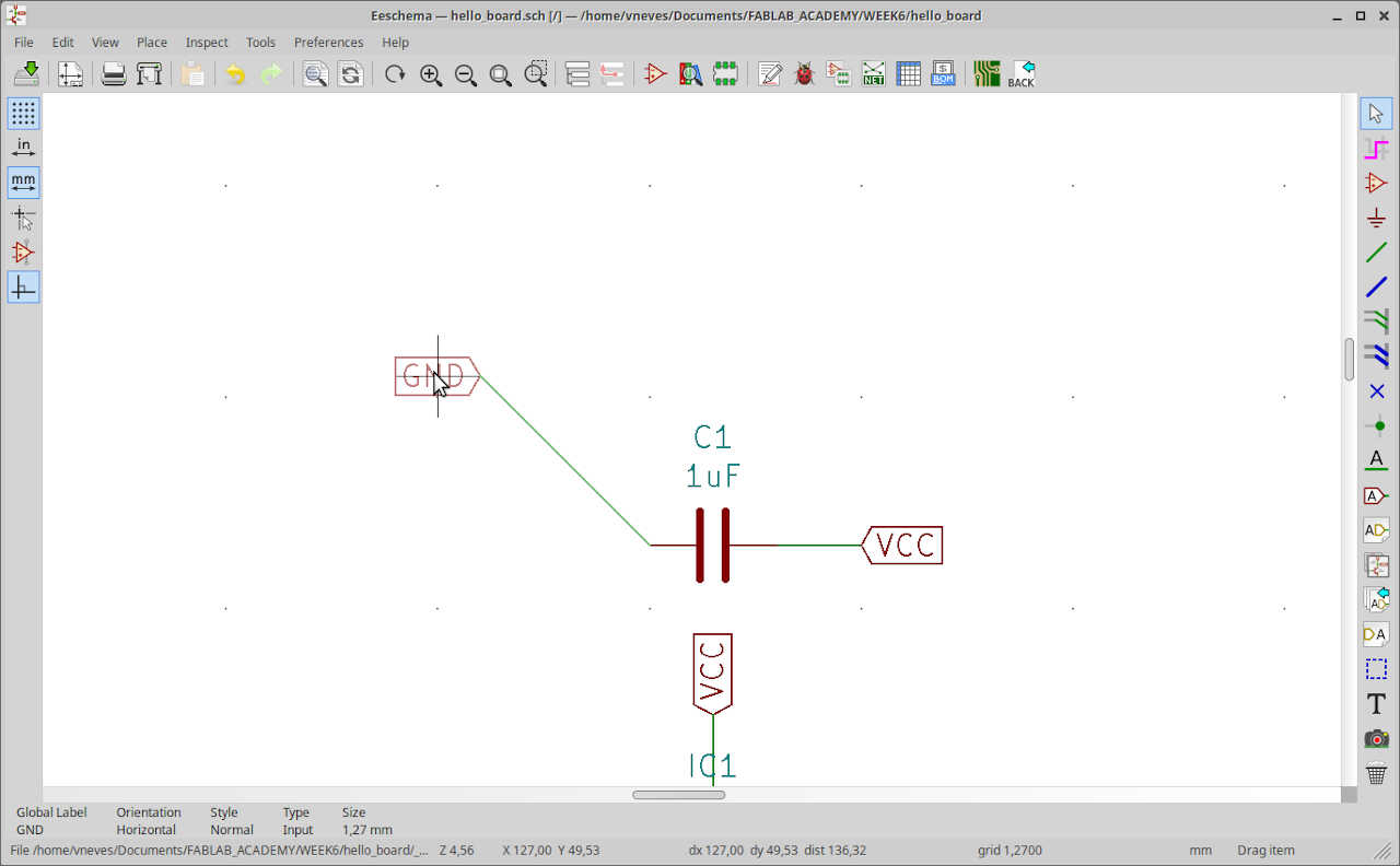
Next, I placed a global label named GND on pin 14 (GND) of IC1. To do this, I clicked on the global label icon (9th icon on the right, from the bottom up), chose a place near pin 14 and wrote GND on the Global Label Properties and with Down orientation.
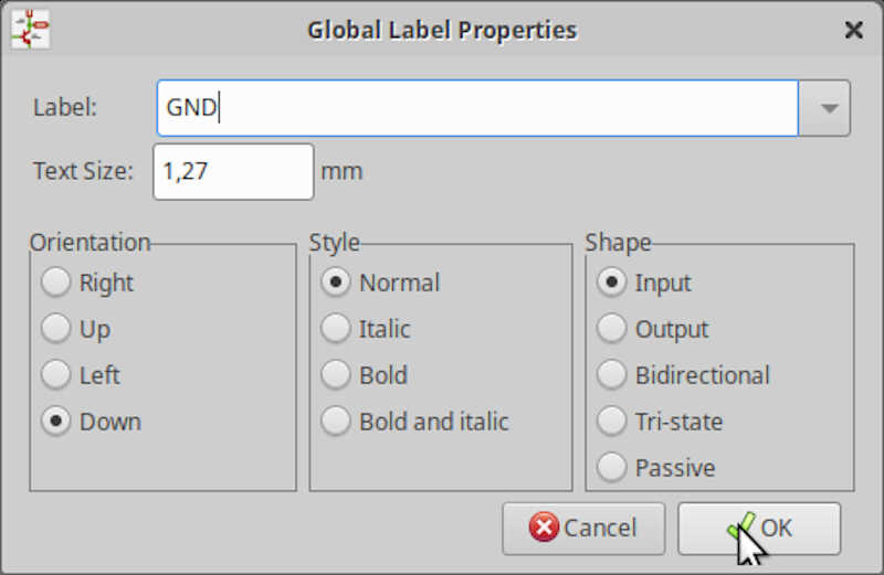
Finally I placed a wire between the GND Label and pin 14 of IC1 by clicking on the wire icon first (5th icon on the right) and clicking on the terminals of both symbols. In fact you don’t need to place wires here. Just add the label directly to the pin ;)
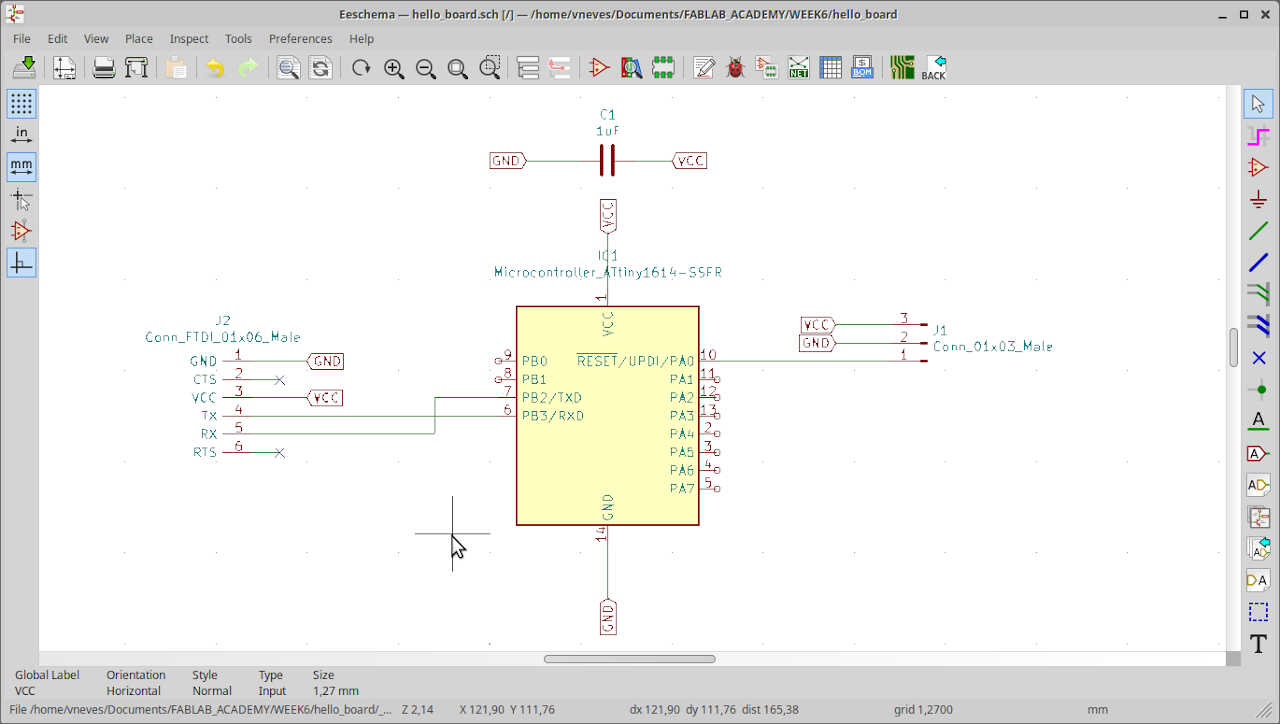
Then, I added two male connectors: a 1x06 male FTDI connector (J1) and a male UPDI 1x02 connector (J2). This way we can communicate with the IC with both FTDI and UPDI communication protocols. Take care to choose only fab components. You can rotate your components with the R key. I also added a 1 \(\mu F\) capacitor that will be used as a decoupling capacitor to stabilize the voltage provided to the IC. I’ll call it C1 and add a value of 1uF. To add this value, I clicked on the C character below to the C1 one and edited it.
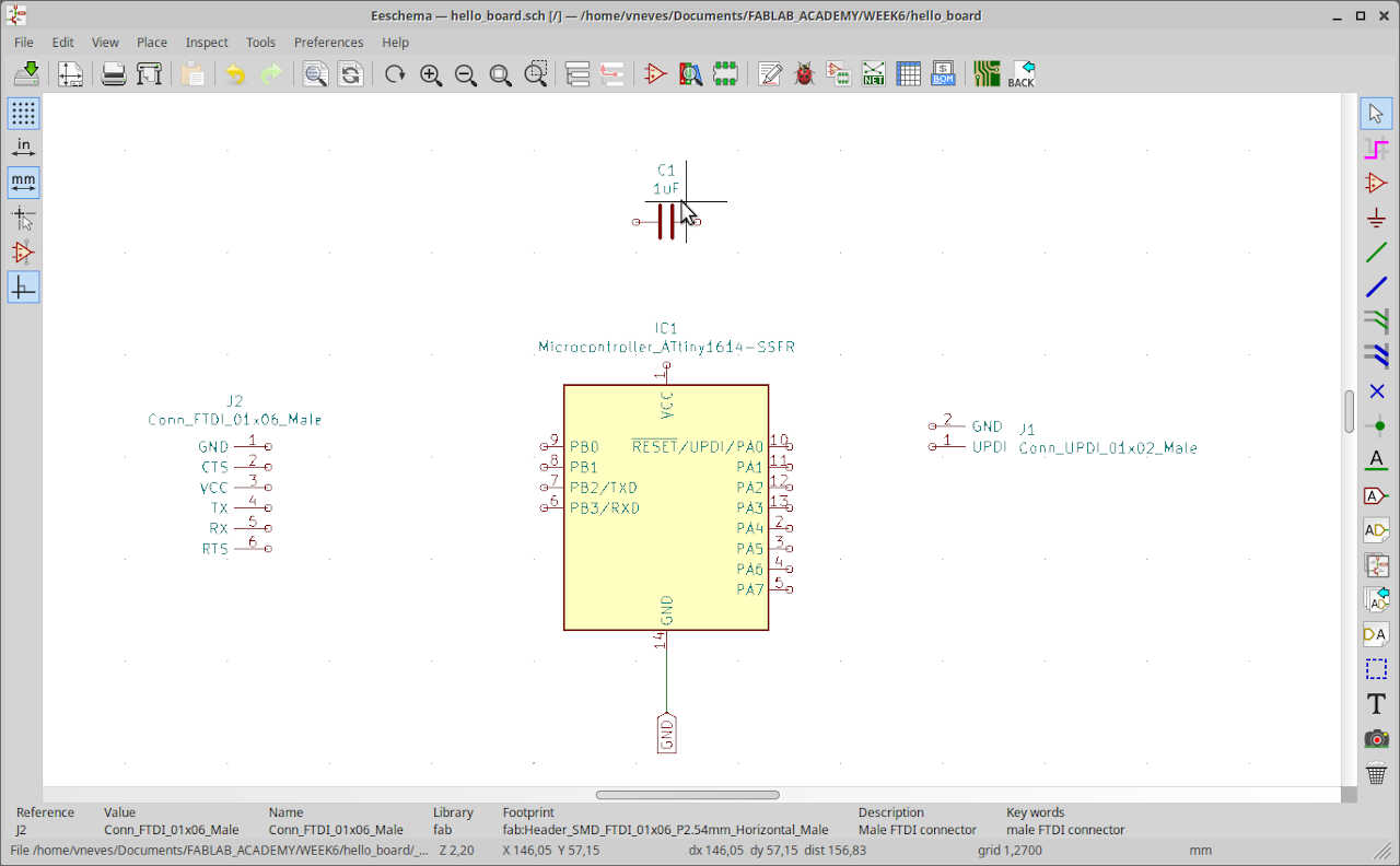
Now I will connect everything, closely following Neil’s board shown above. First I added another global label named VCC so that I could place all VCCs together.
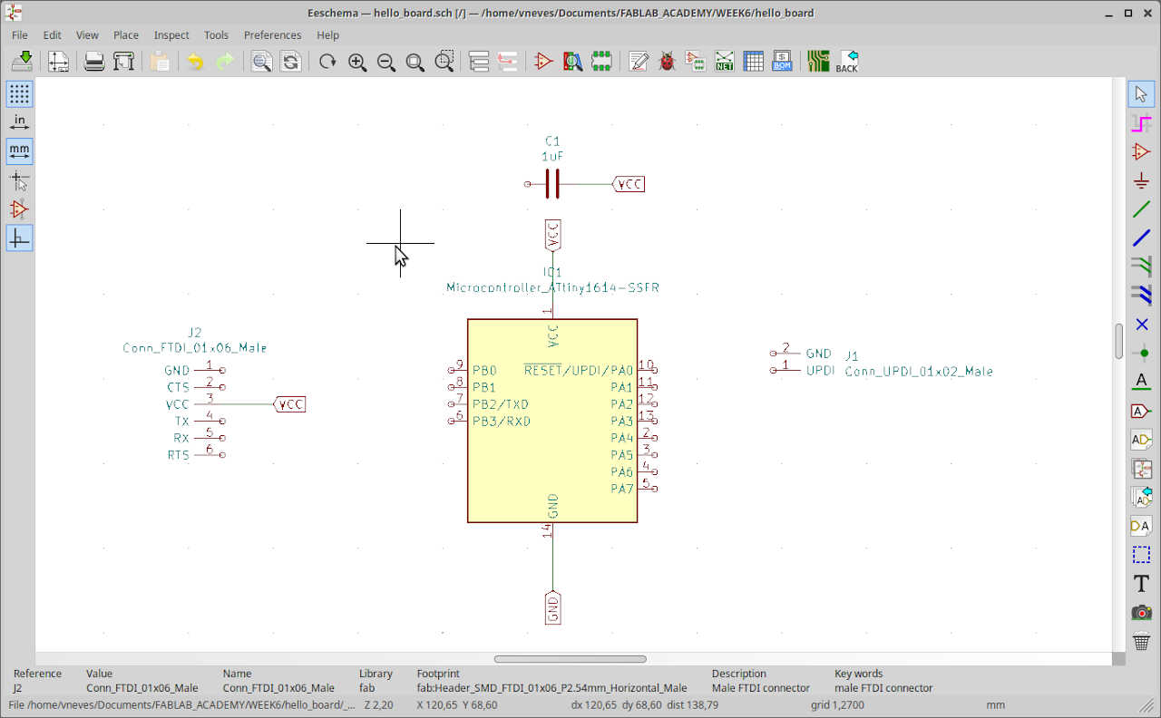
Then I connected everything else. I also replaced the 2-pin connector with a 3-pin one. Note that you can also flag non connected pins using the Place no Connection Flag tool. It is the 9th symbol on the right, the blue cross. I will not place this flag on the IC because I want to add some stuff on it yet. I’ll leave that to the end.
Another very useful command is drag. Instead of moving you can right click on the component and choose Drag or by left clicking on the component and using the shortcut G. Differently from moving, the drag preserves the connections.
Redesigning the 1614 board
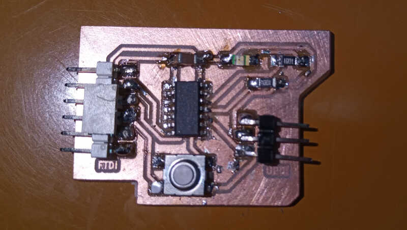
It is time to redesign the board! I’ll add a press button and a LED. Both components will have a 1 \(k \Omega\) resistor in series to limit the current that goes through them. I picked the components from the fab library and added them to the board in the following way:
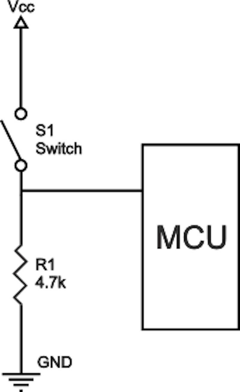
- The press button will be connected to PA1 with a 1 \(k \Omega\) pull down resistor. This means that when the button is pressed the signal will be the VCC signal and when the button is released the signal will be zero, as the resistor pulls down the input voltage to zero. The following picture shows the diagram that will be implemented.
- The LED diode will be connected to PA2 with a 1 \(k \Omega\) resistor in series. The resistor is here to limit the current provided to the diode, thus preventing its burnout.
I chose these two pins to place the components on different sides of the board. The final diagram is shown in the following picture.
From here, I generated a netlist to export the components and its connections to the PCB Layout Editor.
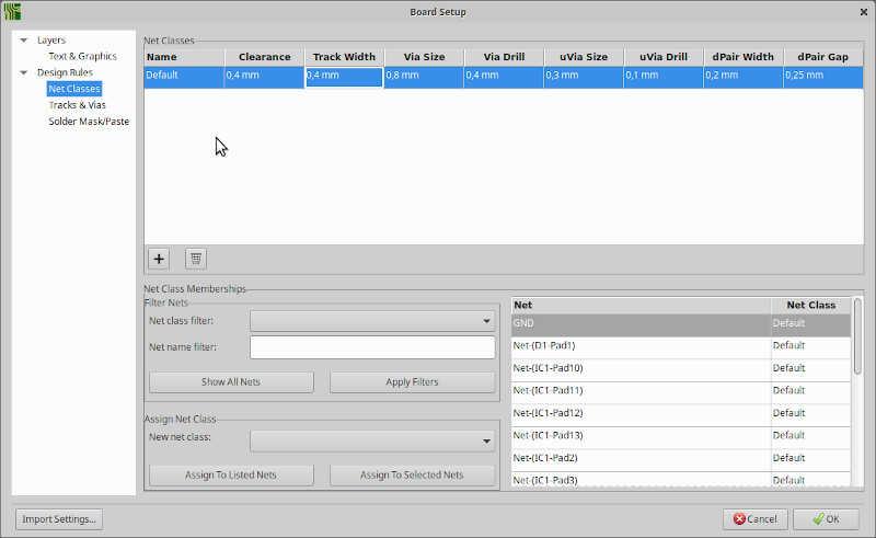
Now I need to set up the design rules. To do that I ran the PCB Layout Editor and clicked on File/Board Setup. From here, I changed both Clearance and Track width to 0.4 mm.
Then, I loaded the Netlist and clicked on Update PCB.
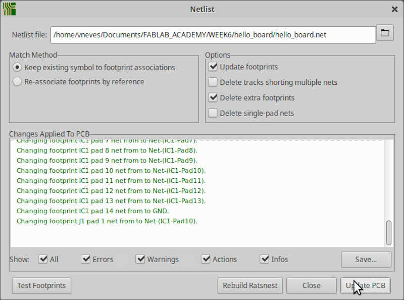
All the components and their connections appeared on the PCB board layout.
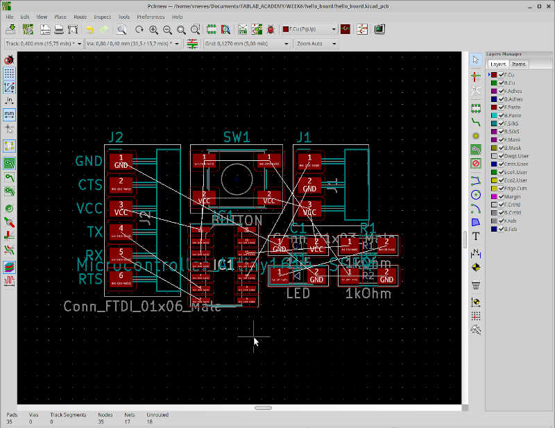
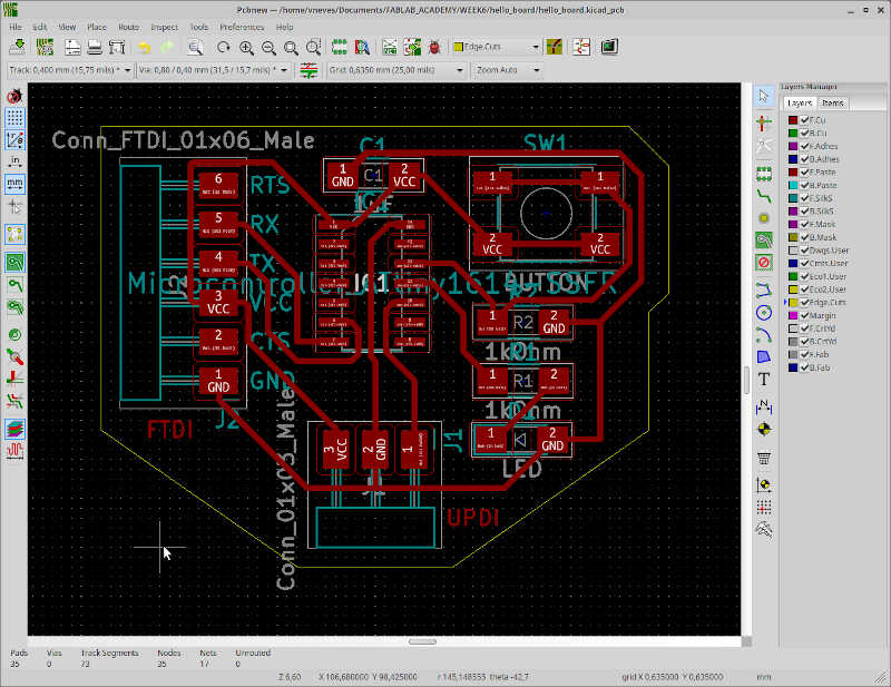
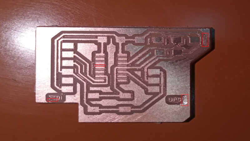
Now I need to arrange the components according to the design rules. After a while I ended up with the following design. I also added the words FTDI and UPDI near their respective connectors by using the Text Tool (the 7th icon with a big T from the bottom on the right). This design was inspired by the very helpful pages of Adrian’s Adrianino page and Fablab Kali Electronics designs.
Unfortunately I noticed that my 1x03 connector that I did on week04 and this one have their pins switched. :O. When I changed the VCC pin to 1 and the UPDI data pin to 3 I could not make all the connections anymore so I had to reconfigure the design of the board.
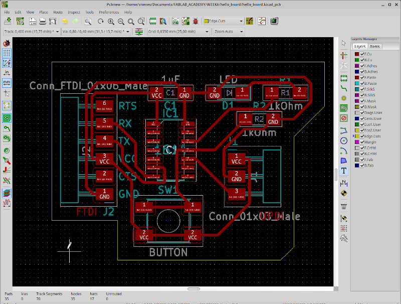
Now pin 1 is VCC and pin 3 is the UPDI comms pin. This change would bring other problems as we will see later on. :\
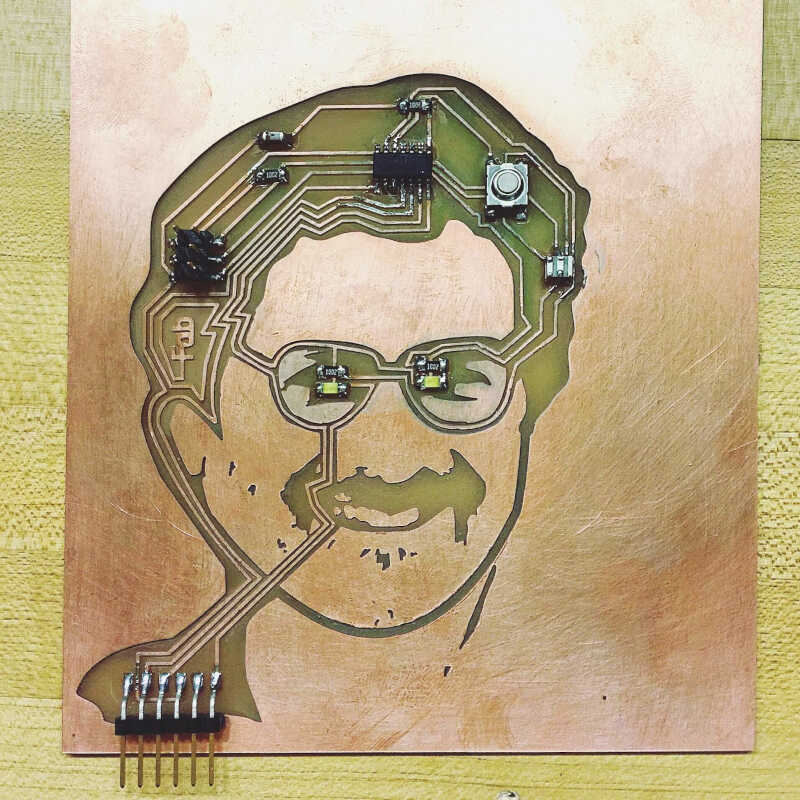
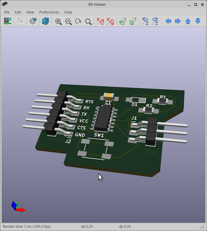
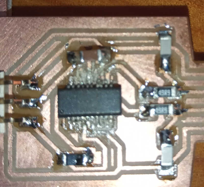
The final board in 3d looks like this. The button and the led are missing, I guess there are no 3D representation of them at this time. I am now ready for the board production!
6.2 Hello Board Production
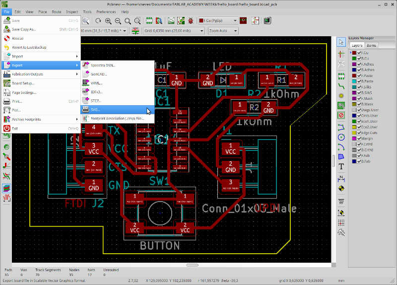
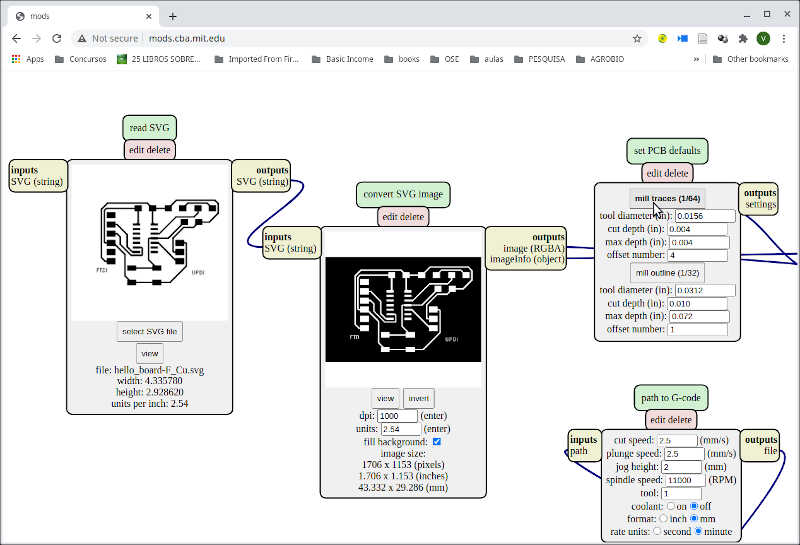
Before producing the board I needed to export the necessary traces and interior .svg files to feed in MODS in order to obtain the GCODE files for milling.
In the Kicad PCB Layout Editor I clicked on File/Export/SVG.
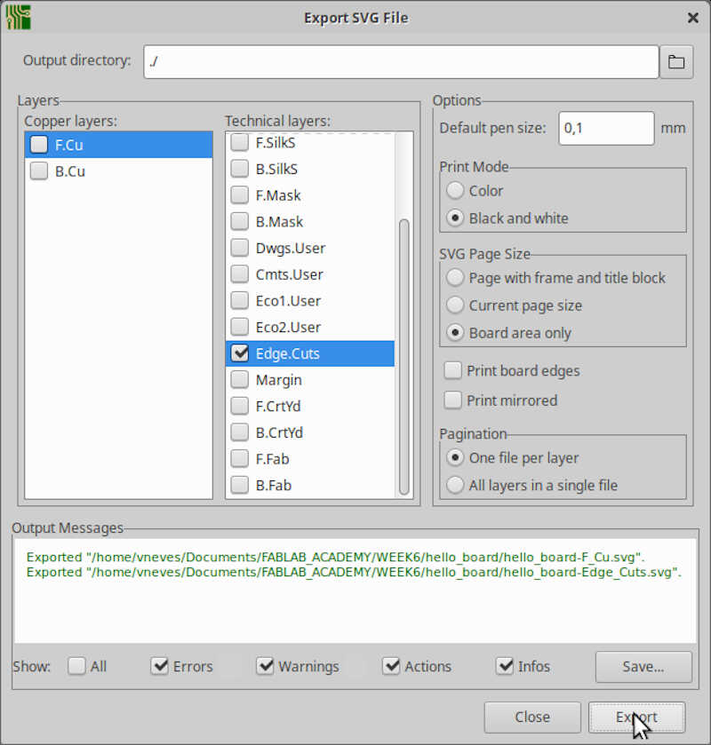
Then I exported two files:
- The first one with the traces, using the options shown in the following picture
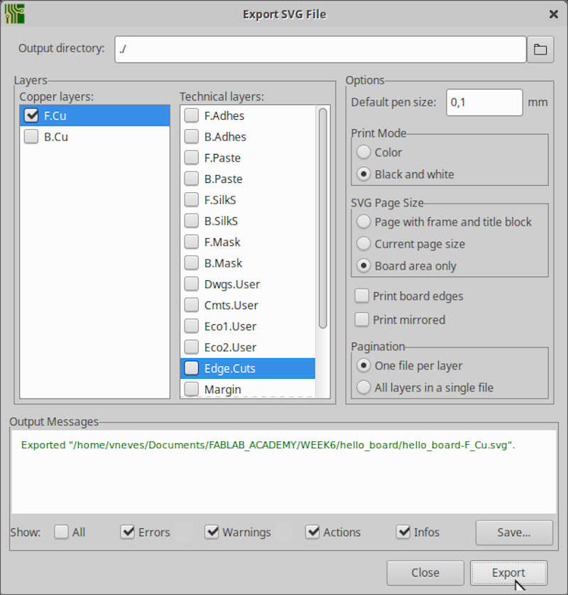
- The second one with the interior, choosing only the
Edge.CutsTechnical layer.
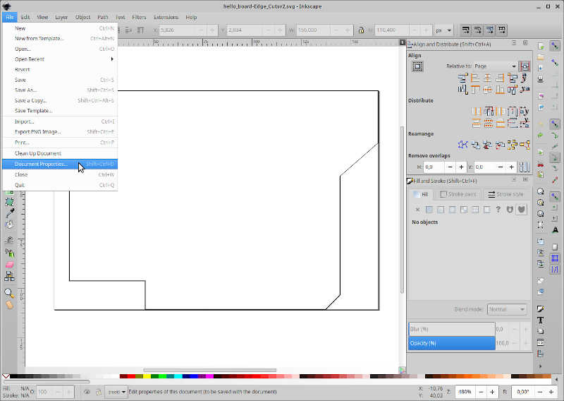
Before importing the files to MODS I needed to change the interior file, because the edges in the limit of the image will not be recognized by MODS. I also need to fill the interior with the black color. I opened the file in Inkscape and clicked on File/Document Properties.
Here, I added one mm on Width and Height of the page.
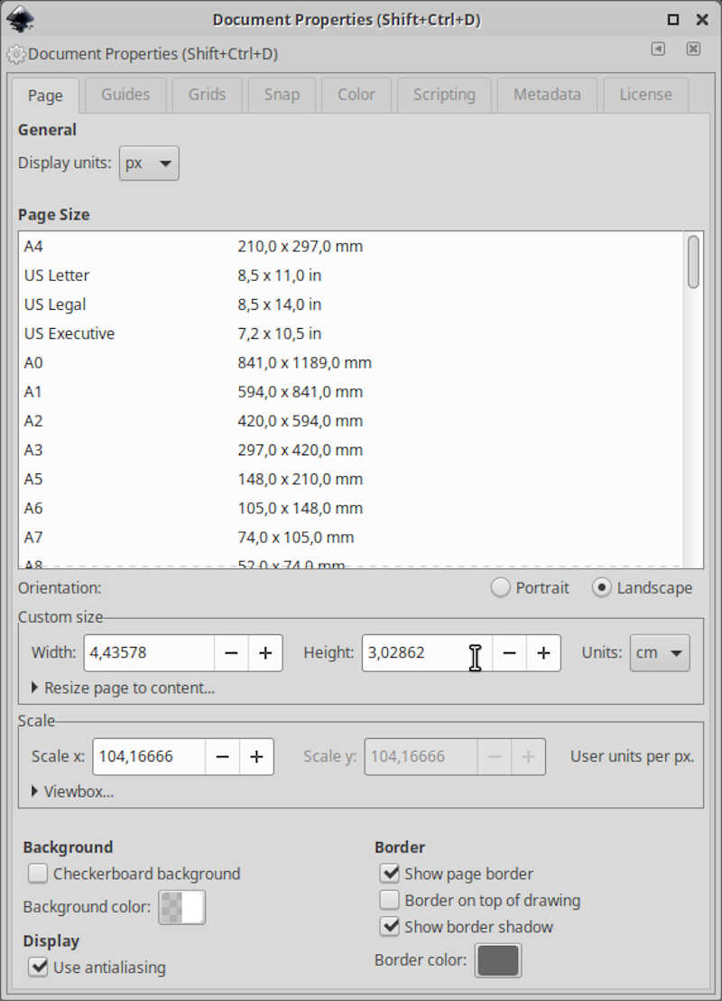
This action enlarged the canvas by 1 mm.
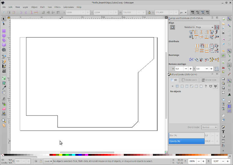
Then, I centered the figure using Align and Distribute (shortcut: CTRL+SHIFT+a) and clicking on Center on vertical axis and Center on horizontal axis. This is always done Relative to: Page.
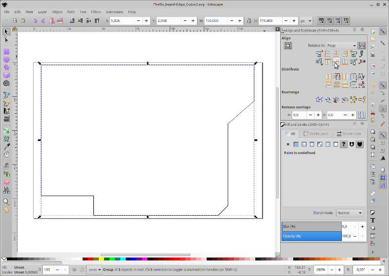
This action was needed to separate the board edges from the canvas borders. When doing the milling I need to bear in mind that I may need some adjustment not to mill diretly into the traces due to this 1 mm change.
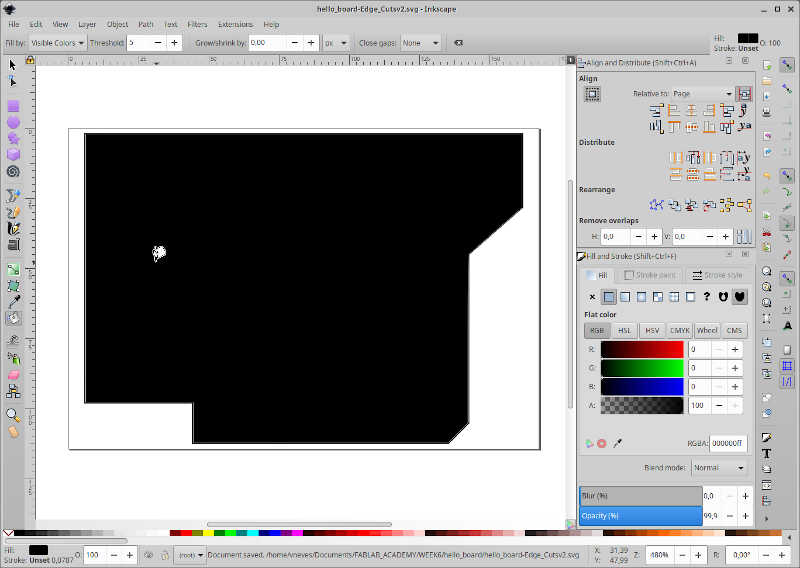
Finally, I had to fill the interior of the board with ink (Fill bounded areas tool - shortcut *U*). I chose black, so I will need to invert the colors within MODS later, because it recognizes the edges within the white borders.
From here, I went to MODS, and chose with the RMB programs/open server program/G-code: mill 2D PCB svg.
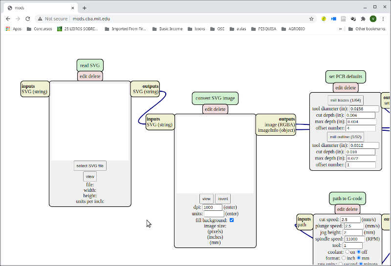
Then I opened the traces .svg file, inverted it on the convert SVG image box, and chose mill traces 1/64 on the set PCB defaults box.
The chosen parameters for mill raster 2D and path to G-code boxes are shown in the following picture.
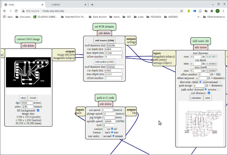
Note: Here I used offset stepover: 0.7 because I wanted to observe if having a greater offset would improve the milling (it didn’t!).
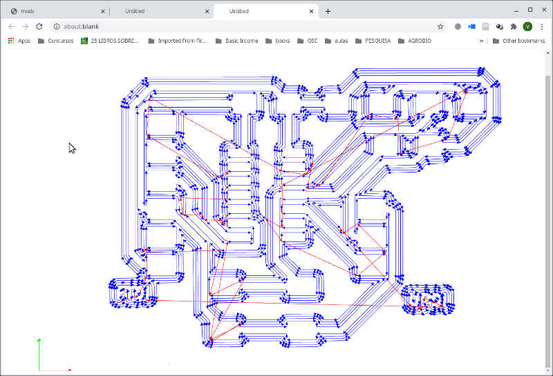
Finally I clicked on calculate on the mill raster 2D box to obtain the .nc GCODE file.
For the interior file I followed a similar workflow. I chose the modified interior .svg file, inverted it, and chose mill outline 1/32 on the set PCB defaults box.
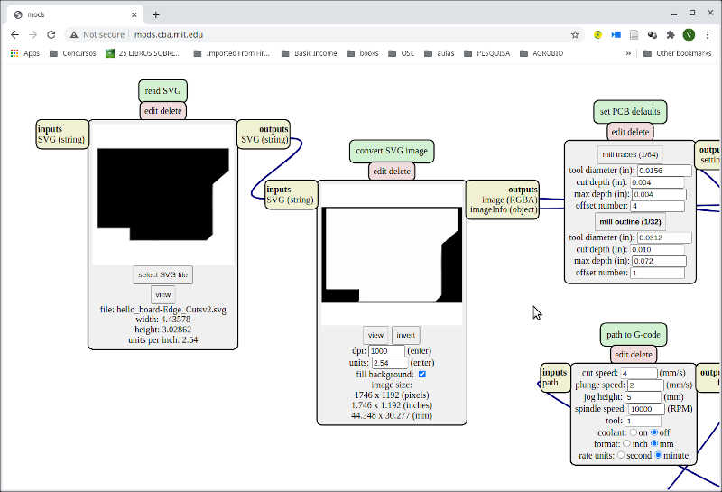
Then I chose the parameters as shown in the following picture…
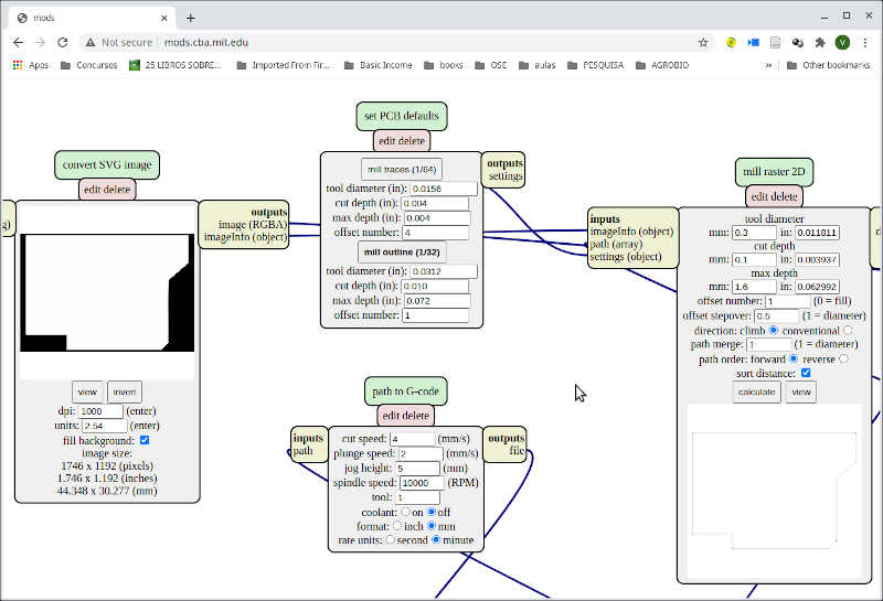
…and clicked on calculate to obtain the .nc GCODE file.
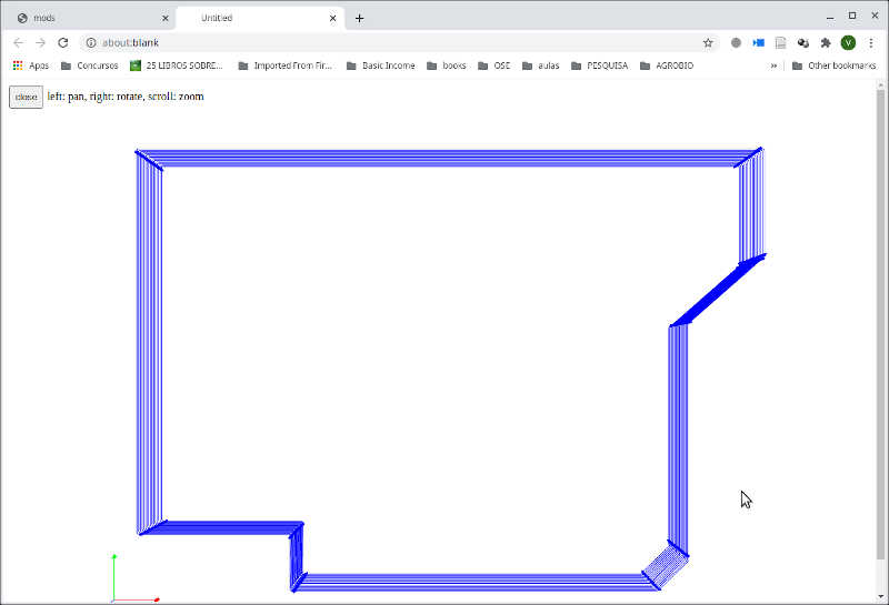
From here I went down to the workshop to mill the board.
I followed the electronics production workflow of week04. I opened Candle and first loaded the traces file…
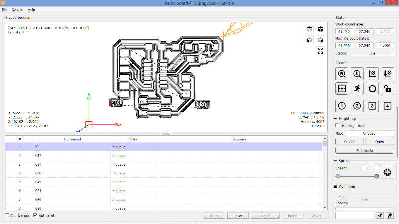
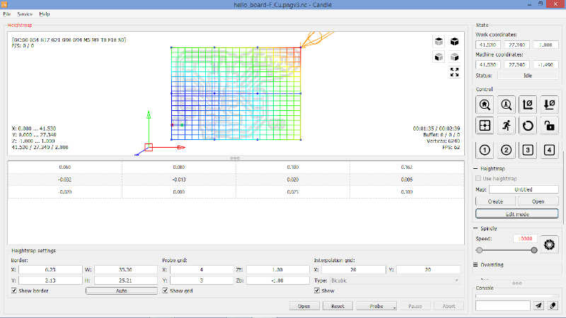
…did the auto-leveling routine and applied it to the board…
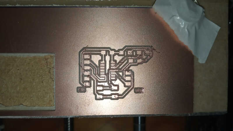
…and obtained the following board.
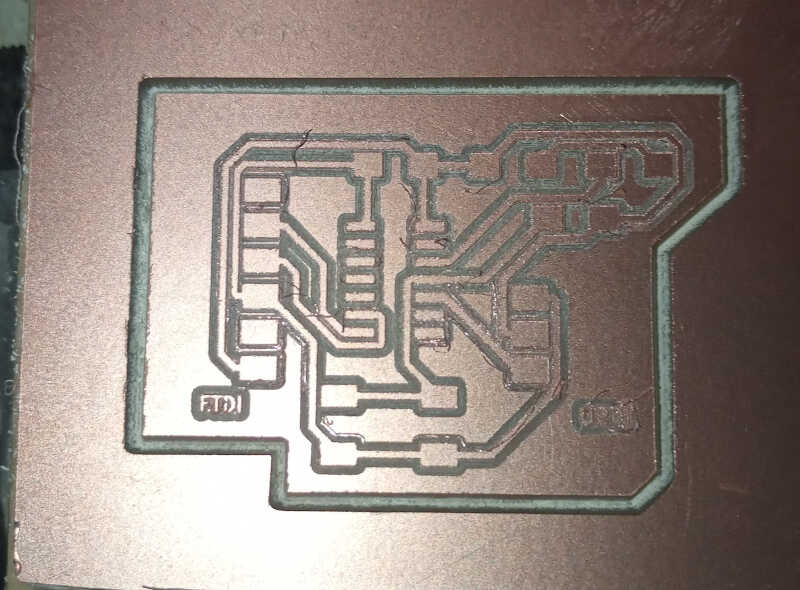
I observed that there were a lot of unmilled areas, as shown in the following picture, and my hypothesis is that the 0.7 threshold for the offsets was too high.
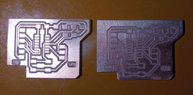
To fix this, I repeated the process, but this time with the usual 0.5 value for the offset stepover parameter. This time the milling came out much better. :)
After cleaning up with the inox wool, I could compare both boards. I chose the latest (on the right hand side) to place the components.
First, I lined up the components I would use. Ok, I didn’t use a 3 pin female connector but a male one and I already had soldered the MC when I noticed it :) I had to bent the 1x03 pins a little so that they could sit on the board.
This time I tried a different technique to solder the MC. First, I placed solder in all pads…
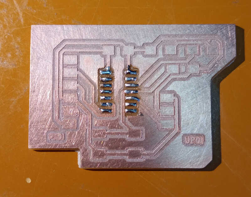
…then I soldered pin 1 (top left), then pin 8 (bottom right) to fix it and finally everything else. In general I just placed the solder iron for 5 seconds on each pin to let the solder make the connection to the pins. It worked quite well!
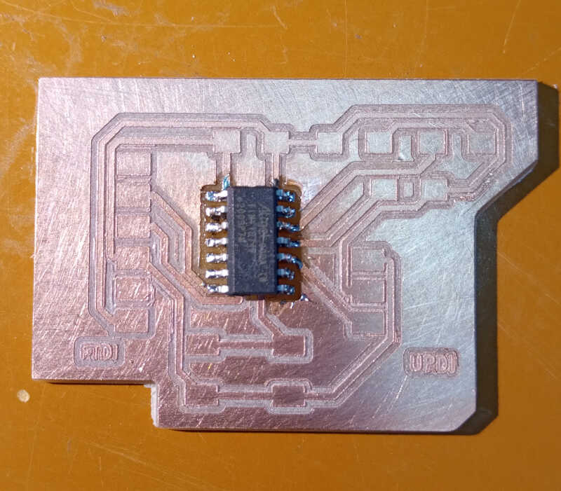
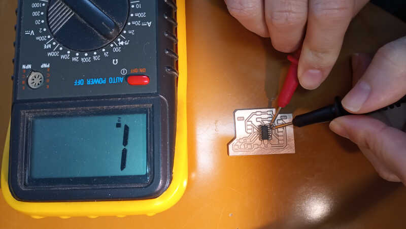
I checked for continuity above and below the pins and between the pins and on the traces they are supposed to make contact with. I also checked the continuity of VCC and Ground tracks/pads.
When everything checked out ok, I went on to place the other components. Yes I know, it doesn’t look so good…I need to practice soldering more!
6.3 Programming…no…debugging! :O
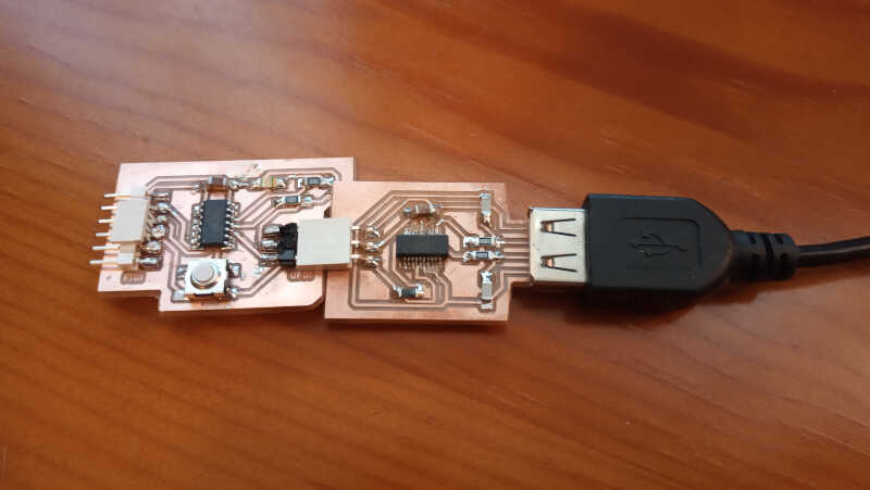
With the two boards produced I could now try and program the 1614!
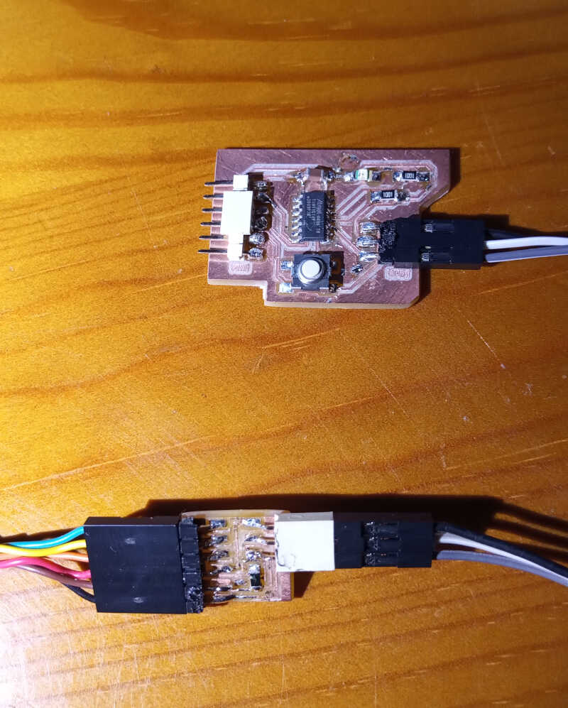
To program the board I just needed to plug in to the USB of my computer and then connect both boards via the UPDI pins, as shown in the picture. And yes…collision alert! They are overlapped and don’t fit well! This is what I was talking about! When I changed the design I forgot to take into account the connection between the two boards! :O
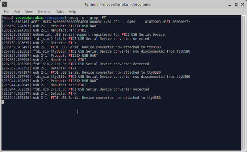
To check the presence of the FTDI board, I typed
dmesg -w | grep 'FT'
and obtained the FTDI data I was looking for. I used grep to obtain only the output related to FTDI.
Let’s try to program then! After doing some research I found some fablab students pages, namely Nadieh’s and Adrian’s and I obtained the instructions and details I needed to try it out! I also used the information contained in the week08 embedded programming page regarding the attiny 1614.
The first step was compiling the hello world program provided by Neil as a test. I copied the .ino file to my computer and installed the latest version of Arduino IDE.
In order to program my ATTiny 1614 later on with this IDE and to use its serial monitor I also installed in it the megaTinyCore libraries. To do this I went to File/Preferences and added the Additional Boards Manager URLs as
http://drazzy.com/package_drazzy.com_index.json
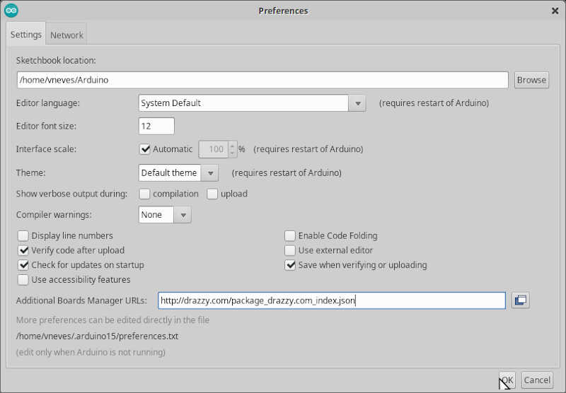
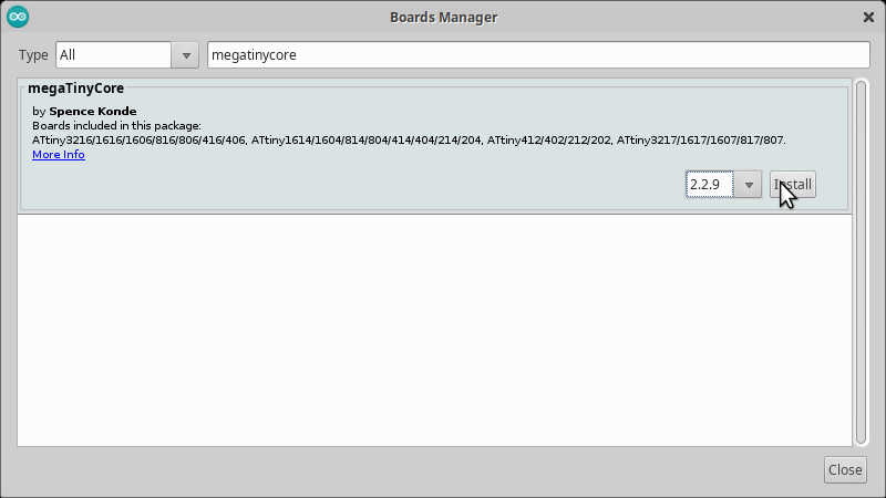
Next, I went to Tools/Boards/Board Manager…
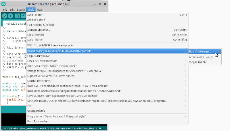
…searched for megatinycore and installed it.
Let’s leave it at that for now. I compiled the program by clicking on the verify icon, the green tick icon on the top left.
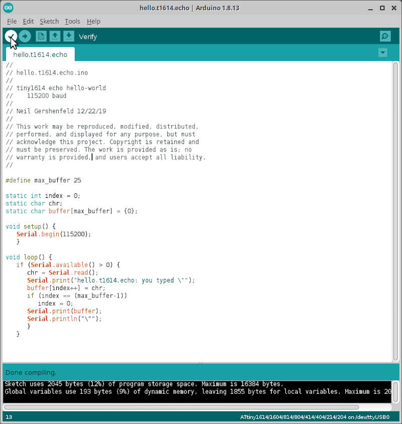
Then I exported the compiled files with Sketch/Export compiled binary to a convenient directory. Here I found the sought over .hex file!
I chose to compile with pyupdi, a python UPDI driver for the tinyAVR and megaAVR devices. To install it I just typed
pip install https://github.com/mraardvark/pyupdi/archive/master.zip
at the command line. I had python 3 and all needed dependencies previously installed on my computer.
With this file in hand and with the information of the USB port (ttyUSB0) given by the dmesg command as well as the name of my MC, I typed in the command line
pyupdi -d attiny1614 -c /dev/ttyUSB0 -b 57600 -f hello.t1614.echo.ino.t1614.20c0.u5V.mD0.hex -v
where c is the COM port, b is the baud rate, f is the hex file you want to program and v is a verbose flag for pyupdi.
Unfortunately it failed…and I couldn’t fix it…this day! The output shows a
link UPDI not OK
and
UDPI initialisation failed
at the end.
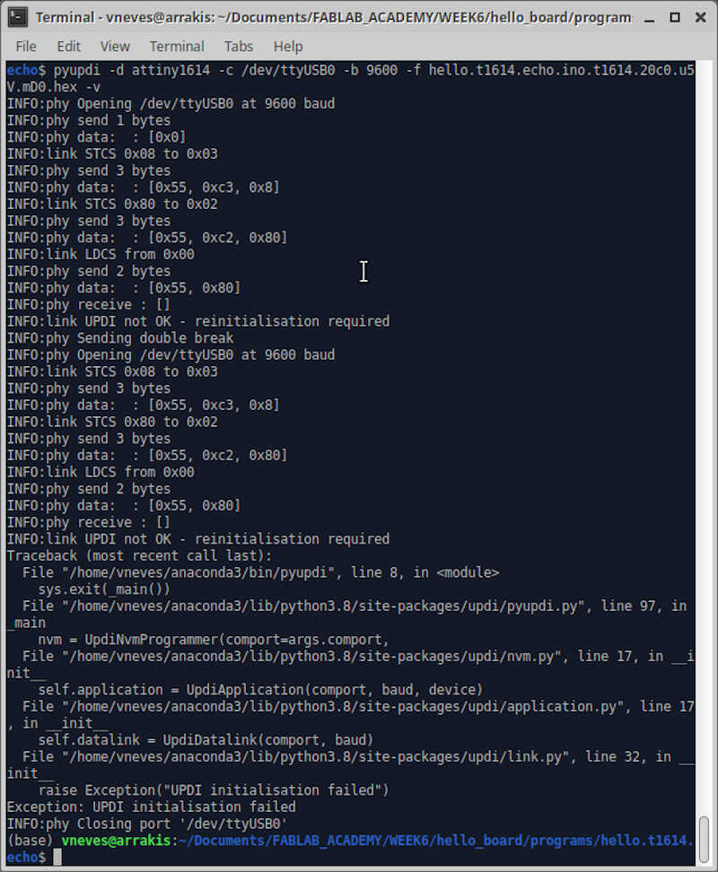
To fix this at the time, I tried to upload it with Arduino IDE (failed, outputting a similar error) and then I tried to debug both boards.
In the FTDI board I found there were three pins making contact. They are so close together! I drove them apart (again!) and tried to insure they would ever never touch again by driving a wedge with the cutter between them (I know…horrible and cruel stuff!).
After triple checking everything was ok, I move to the other board and everything checked out ok. So both boards were behaving in terms of continuity.
Then I checked the voltage of my ATTiny board…and it was irregular giving values at the 5V input pit and at pin 1 of the MC of 0.5 to 3.5 volts. So something was off!
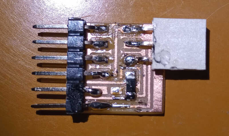
After a while I concluded (?) the problem was in a cold solder in the 1x03 female connector. The picture shows a close up view of the pins and they really are just on top of the solder.
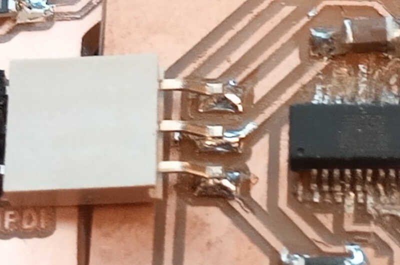
Soon, the connectors went loose and detached from the board, so I need to re-solder them once I finish this diatribe! ;)
To test my “conclusion” (I should politely say hypothesis!) I went on to mill a three pin hello.serial-UPDI.3 board as shown in the week06 Fab Academy page. This way I could connect this board to the provided FTDI cable I have here and to the hello board. I downloaded the board, traces, and interior .png files so I could use them directly with MODS.
I quickly went through the usual workflow with MODS and Candle. The final result was this very tiny board that I show here:
- After the milling
- After sanding the sides and removing some leftover lines with the hand cutter
- After soldering everything
Finally I connected the USB FTDI cable to the serial-UPDI board and this one to my ATTiny 1614 hello board. I checked the 5V lines with the multimeter and everything was checking fine! Note that I had to use the three male-female jumper cables here because the connections between the VCC pin and the UPDI pin on both boards are switched! This was just for test and I can easily do another FTDI-UPDI board with the switched pins.
I went back to pyupdi and typed the command I mentioned before in the command line…
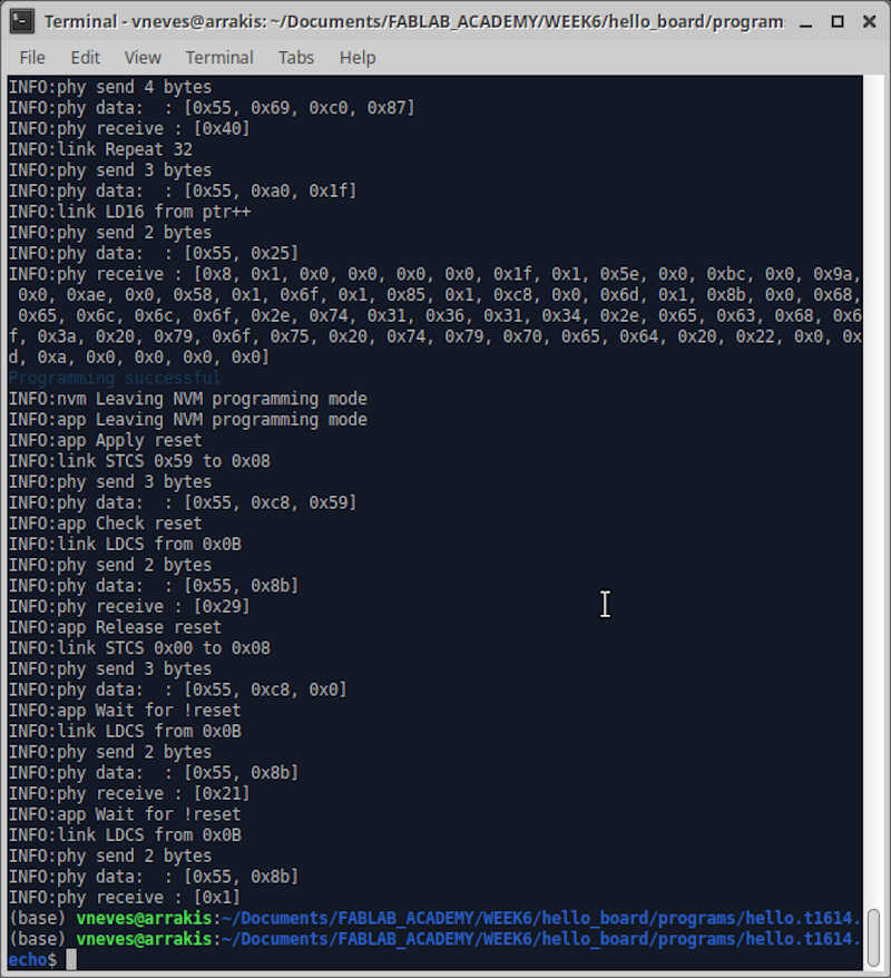
…and IT WORKED! :D The UPDI link was established, the compiled .hex file was transferred to the board in a few seconds and the the Programming was successful! Did it work?
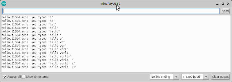
To test it, I opened Arduino IDE and went to Tools/Serial Monitor.
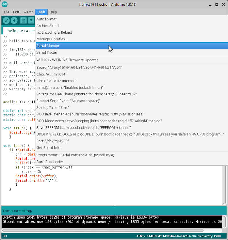
Here, I chose the No line ending option at the lower right corner of the image and typed sequentially
hello world! :)
and the board showed it is alive. Great!
I leave it here for now. More programming on week08 coming up! ;) And I have a FPDI board to debug! :D And also need to learn to solder properly… :P