7. Electronics design
This week I worked on designing an electronic board using Eagle software; a design tool for designing printed circuit boards. I found working in this software was very simple due to its graphical interface which made it easier for a total beginner like myself. You can install Eagle for free from here
When designing a PCB from scratch one must go through a specific workflow as follow:
Schematic diagram > Board Design > Fabrication
You will then need to test if your PCB is working by using the test equipment. For more information click here Below I’ll explain each step and show how I made it.
Pre Designing Step: Loading a Library
Before starting my schematic design I made sure to have the fab library and design rules installed in my software. To do so, I followed the following steps
1- I downloaded both files from here
2- I copied the files and pasted them in their location
Documents > Eagle > Libraries > fab.lbr
Documents > Eagle > Design Rules > fab.dru
3- I opened Eagle > New Schematic > Library (from the tool bar) > Open Library Manager and then I followed the steps as shown in the video Below
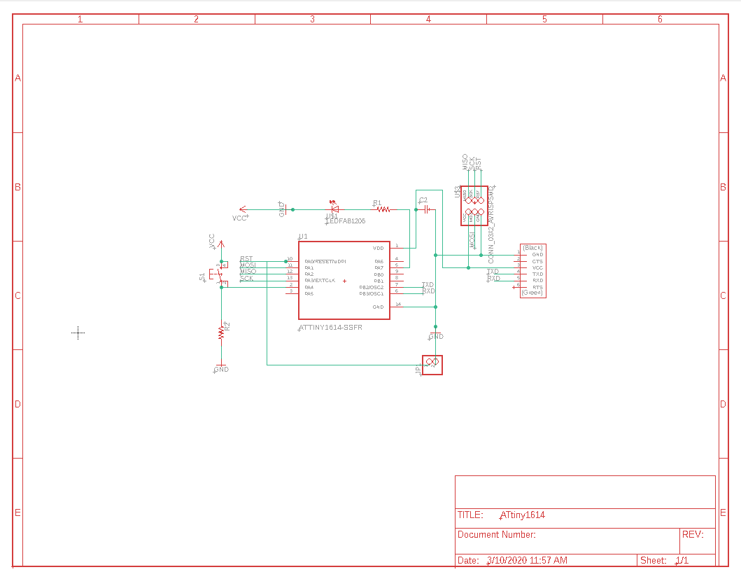
I. Schematic Diagram
A Schematic is a diagram of the components you need in your circuit and lines that represents the connection between them. It is important to know that this diagram doesn’t necessarily corresponds to the organization of the components of the finished physical board.
I chose to redraw the hello.t1614.echo board
To start your schematic design, you will need to add the components of your circuit and then net them together.
The below video will explain the steps I went through to draw my schematic
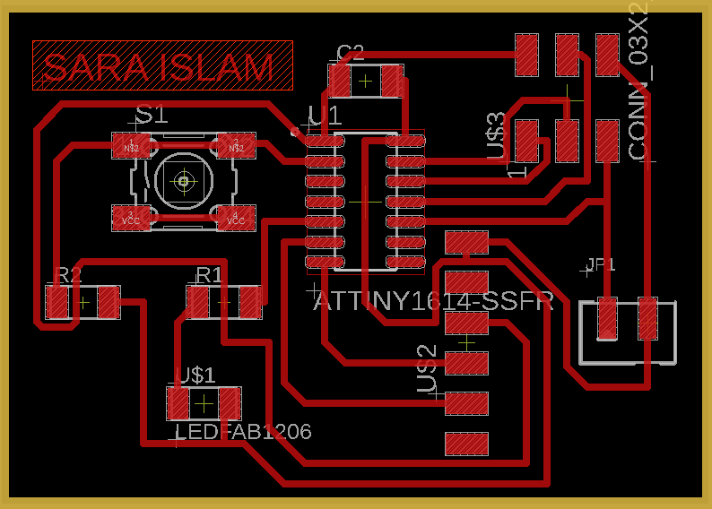
My Schematic Diagram
II. Board Routing
In this step we add the actual wires which connect our components according to the design rules. This step represents the final look of the PCB.
The following video shows how this is done after finishing the schematic.
My Board Design
Problems Faced
when running DRC, I noticed that I had some errors and tried to fix them. Below are examples of the problems I faced and how I overcame them
Problem 1: Clearance Error
Action taken: I increased the space a little bit between the lines that were too close and rearranged the components were necessary
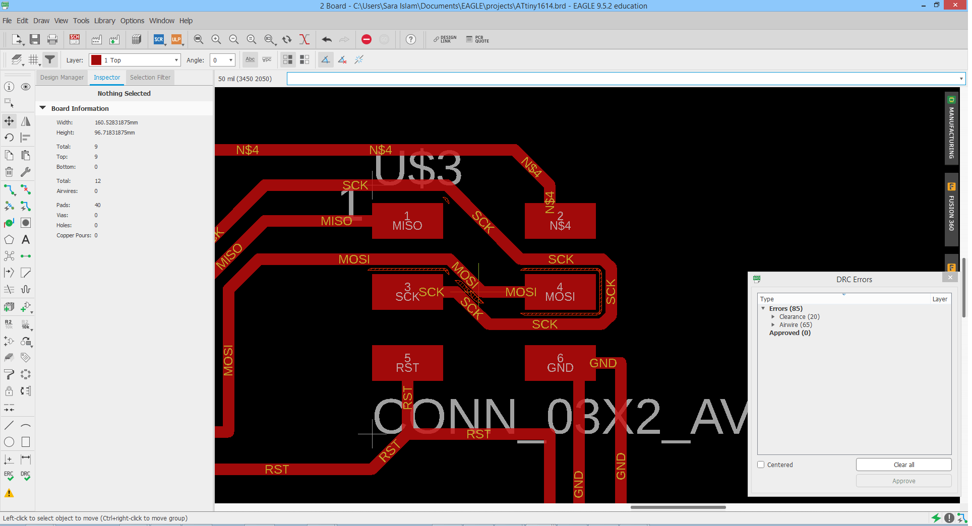
Problem 2: Airwire Error
Action taken: I double checked if I had any airwires but couldn’t find any therefore I just approved them all.

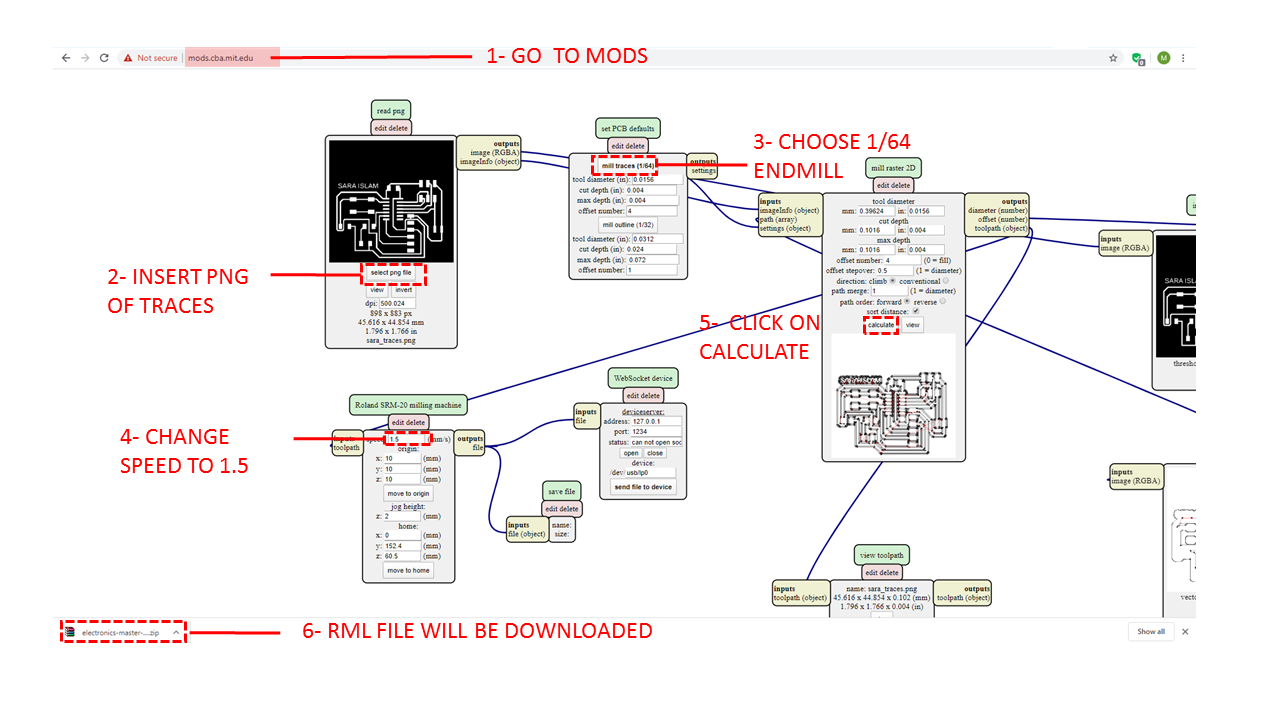
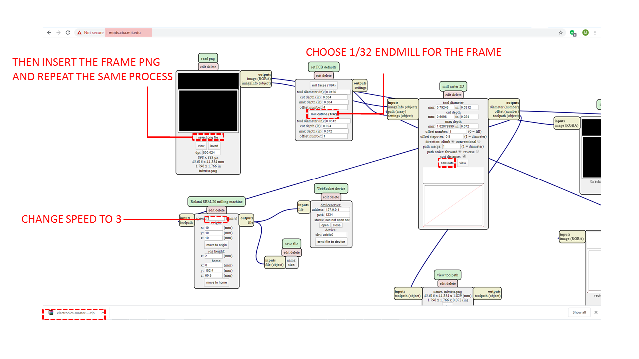
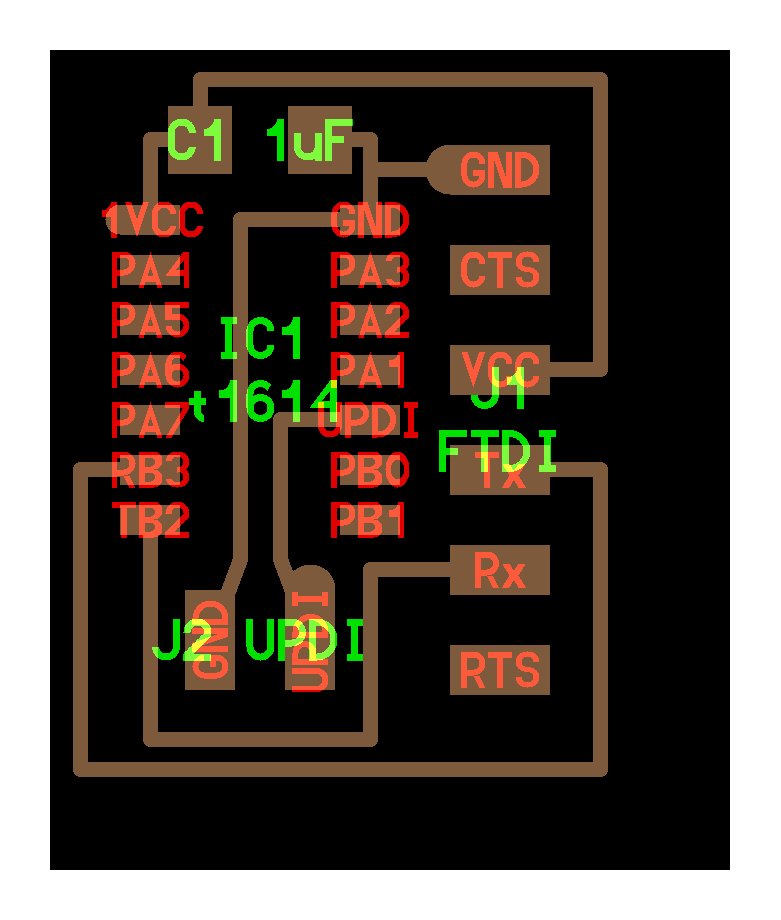
II. Fabrication
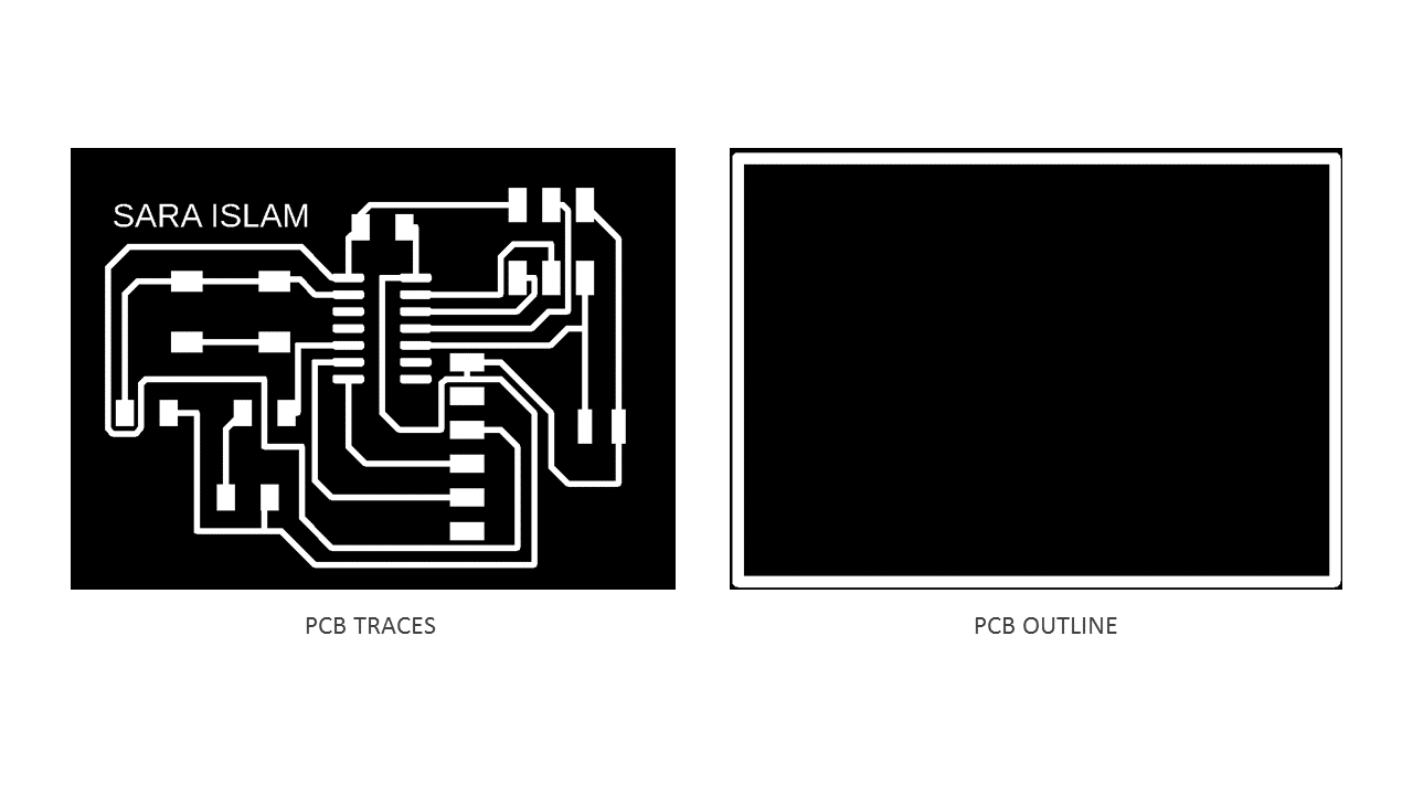
A. Exporting .png files from Eagle
After routing my board I exported it to a png. format in order to be able to mil it. The following video explains the steps in where I exported 2 png. images. The first one is for the traces and the second one for the outline of the PCB.
Here are my exported files
B. PCB Milling
After exporting my files to .png, I then used Mods to convert the files to .rml so the milling machine can take it. I did that for both images with a slight change in the settings. For more details about Mods and the Milling process, go to my Electronics Production Assignment