7. Electronics design
Abstract
Design and fabrication of a microcontroller circuit board and test the circuit board to observe its operation. I have used Autodesk Eagle Version 9.3.1 for the design of the microcontroller board which is described in the Electronics Design schedule. I have redrawn the circuit echo hellow-world board with the addition of a button and LED. Furthermore, group work is done by test equipment in our lab to observe the operation of a newly developed microcontroller board.
Individual Project
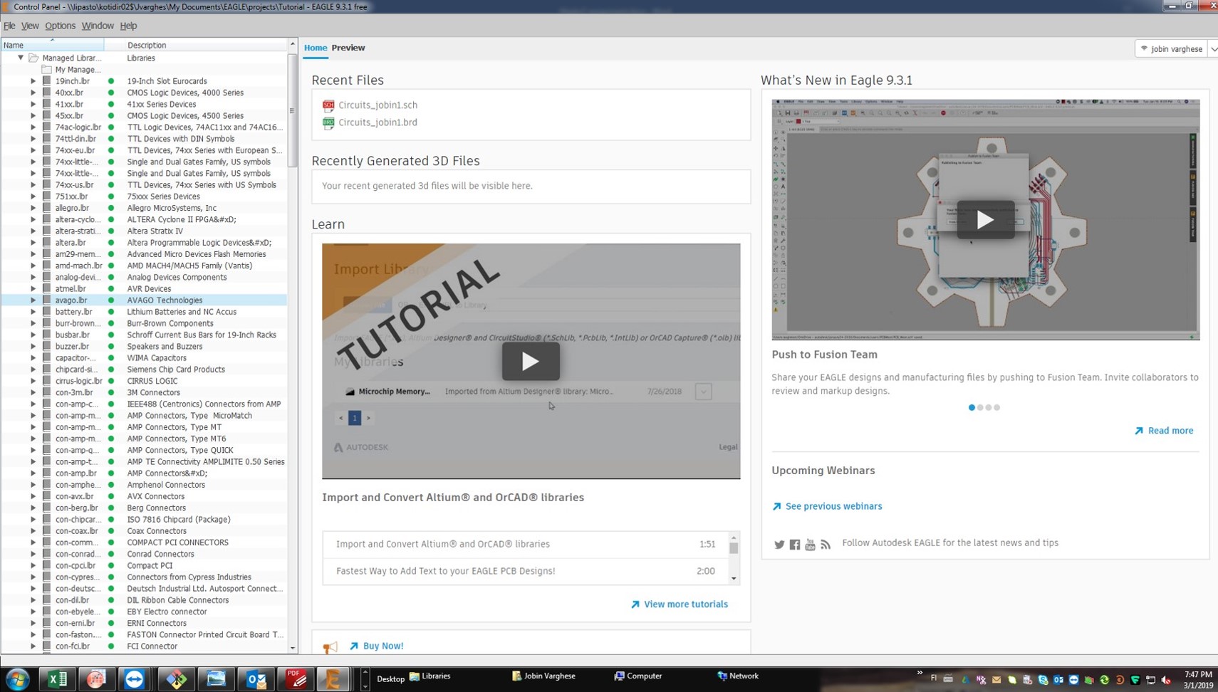
Download the software Autodesk Eagle Version 9.3.1 and install it. I downloaded the fab.lbr from libraries and set the path. See the screenshot below,
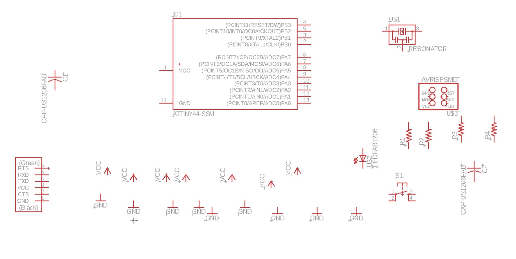
These are the components used in the Eagle FAB library see the list below
- 6MM_SWITCH
- LEDFAB1206
- CAP-US1206FAB C1-1uF; C2-10nF
- RESONATOR (20 MHz)
- ATTTINY44-SSU
- Supply (VCC)
- GND
- RES-US1206FAB (R1-10kohm, R2-1k ohm, R3-49.9kohm, R4-49.9kohm)
- AVRISPMD
- FTDI connector
See the below figure which presents the components for schematic
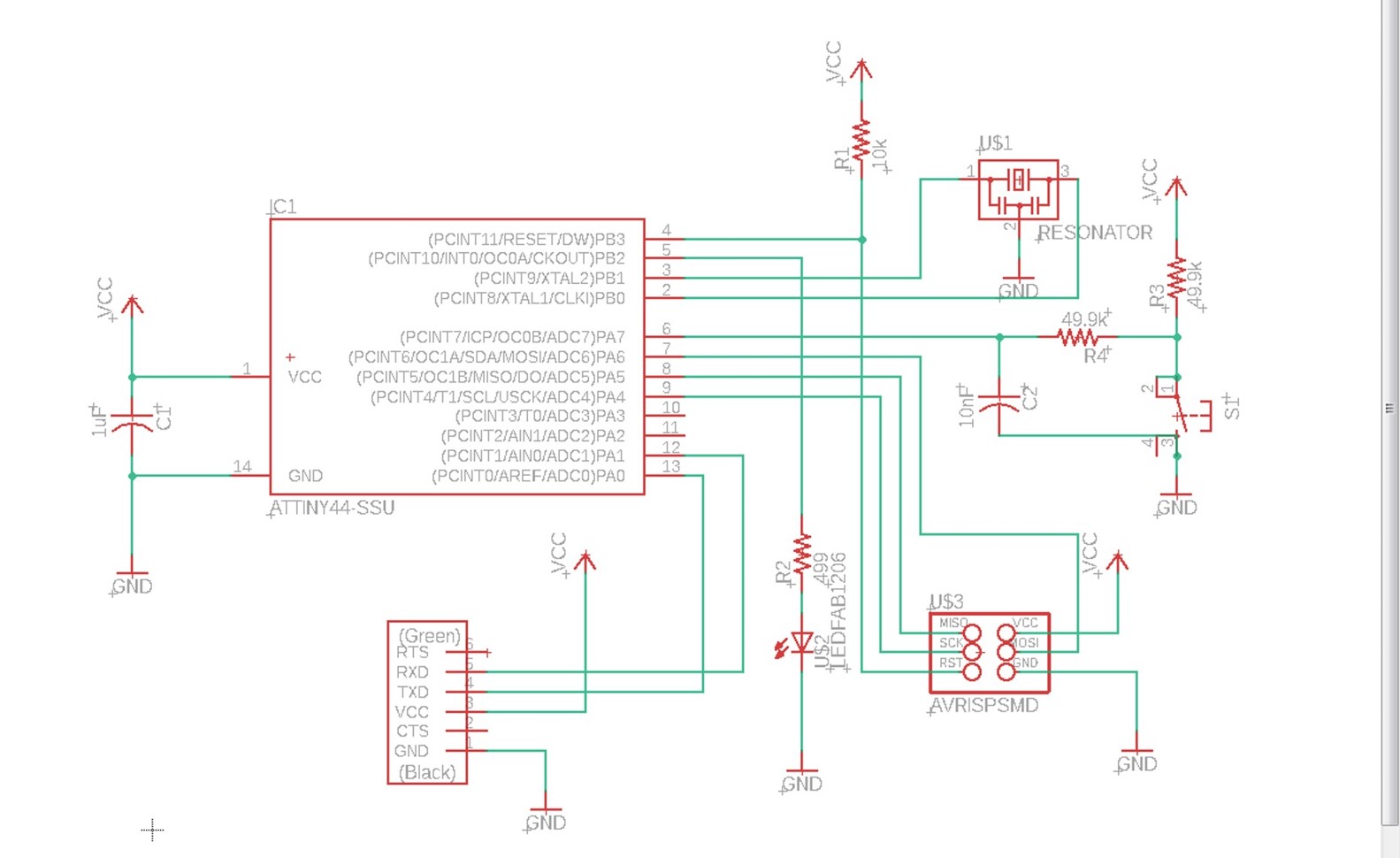
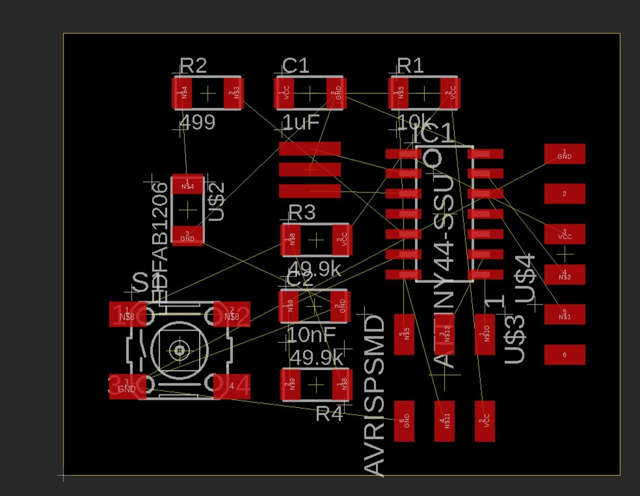
Added all the components GND, resistors, capacitors, VCC multiple times. Draw the line using the Net tool. The green line connected is just connected only two points, while the green dot in the multiple crossing connections. I have finally added components and values based on our list suggested by our local circuit expert Antti. Extra button and LED are also inserted in the controller circuit board as per the assignment requirements. See the connection in the below figure.
Next step is to generate/Switch to board design. See the generated board in the below figure,
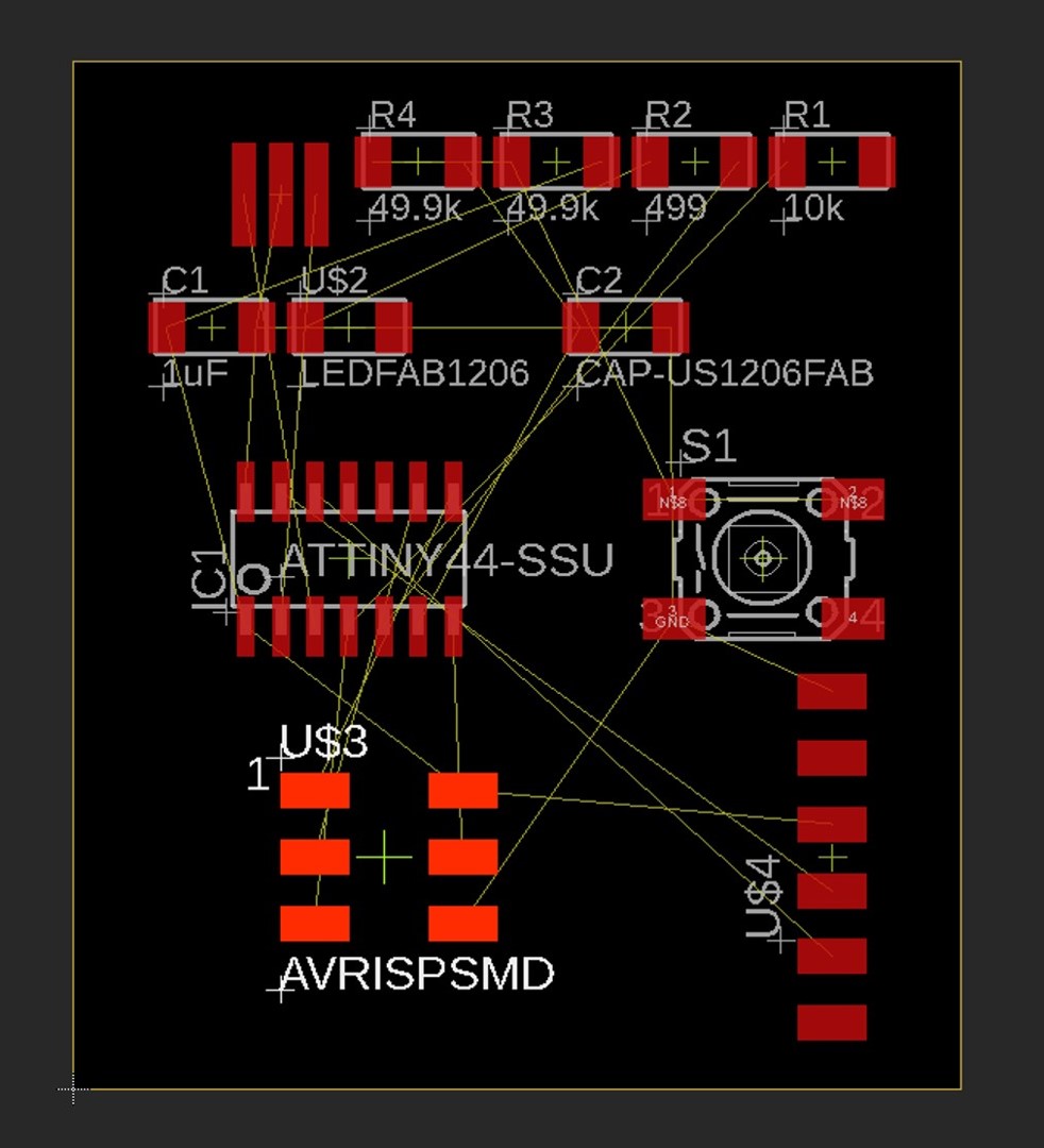
Rearrange all the components before making connections. See my component placements in the below figure
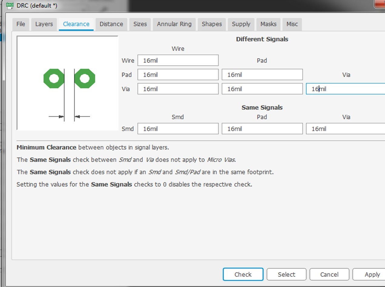
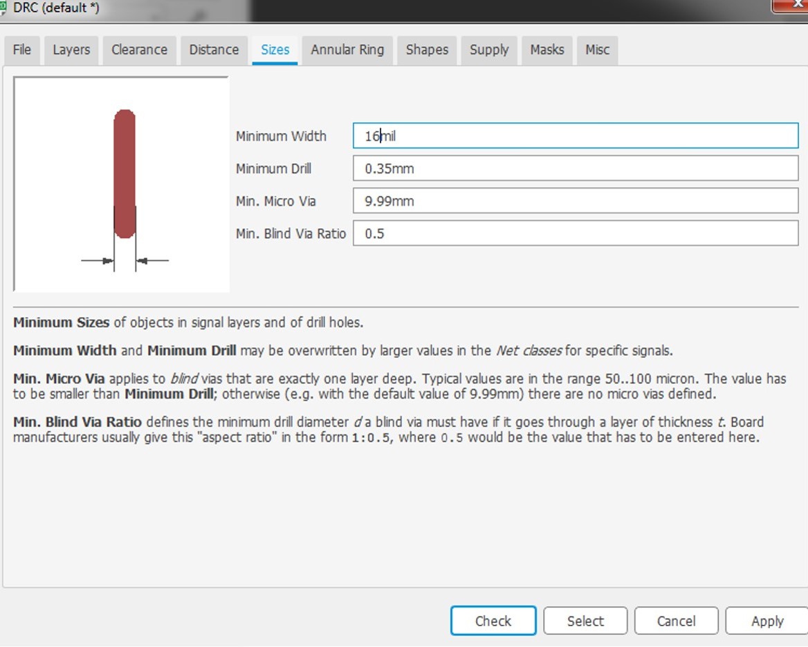
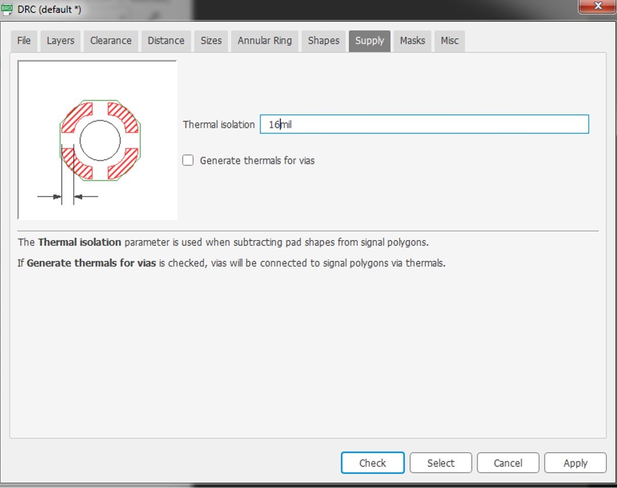
Next step is design rule for routing. Oulu fab lab uses 16 mil suggested for using 0.4 mm V type milling bit. Which is changed in the DRC window-clearance (all changes all default values such as wire, pad, via, different signals and same signals to 16 mill)-Size-minimum, Supply-thermal isolation 16 mill. See the screenshot below,
Clearance
Size
Supply
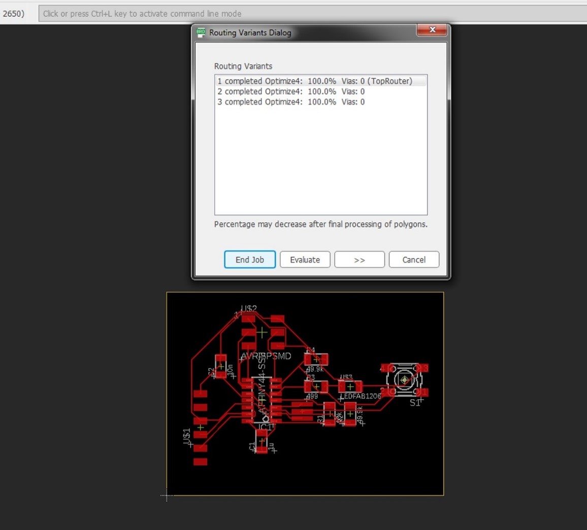
Then, I started to click autoroute and click end job to get 100% perfect connection. See the figure below,
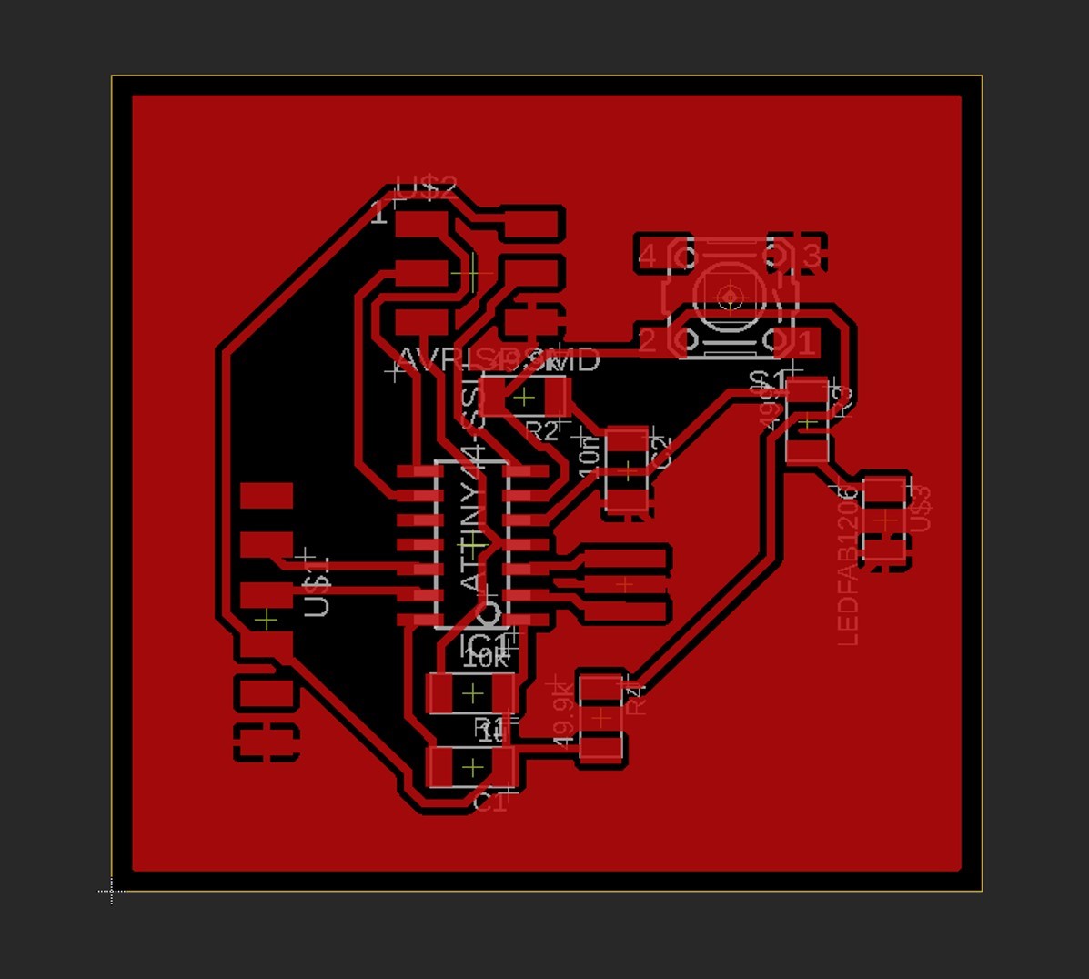
Select polygon icon for the ground plane and name as GND, Followed by Ratnet icon to create the ground. See the below figure when the ground was ready.
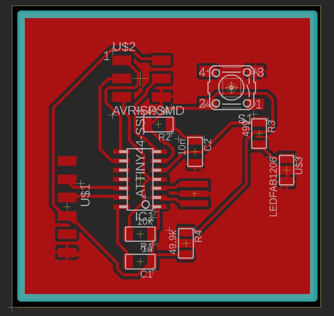
Next step is to prepare interior layout and board. Milling border is adding by using the Line tool and set the line width to 40. Change layer by Top 1 to Milling 46 and draw a blue line to the border edges. See the screenshot below,
When exporting milling image, use a layer to select only top 1 layer for trace and only milling layer for the outline.
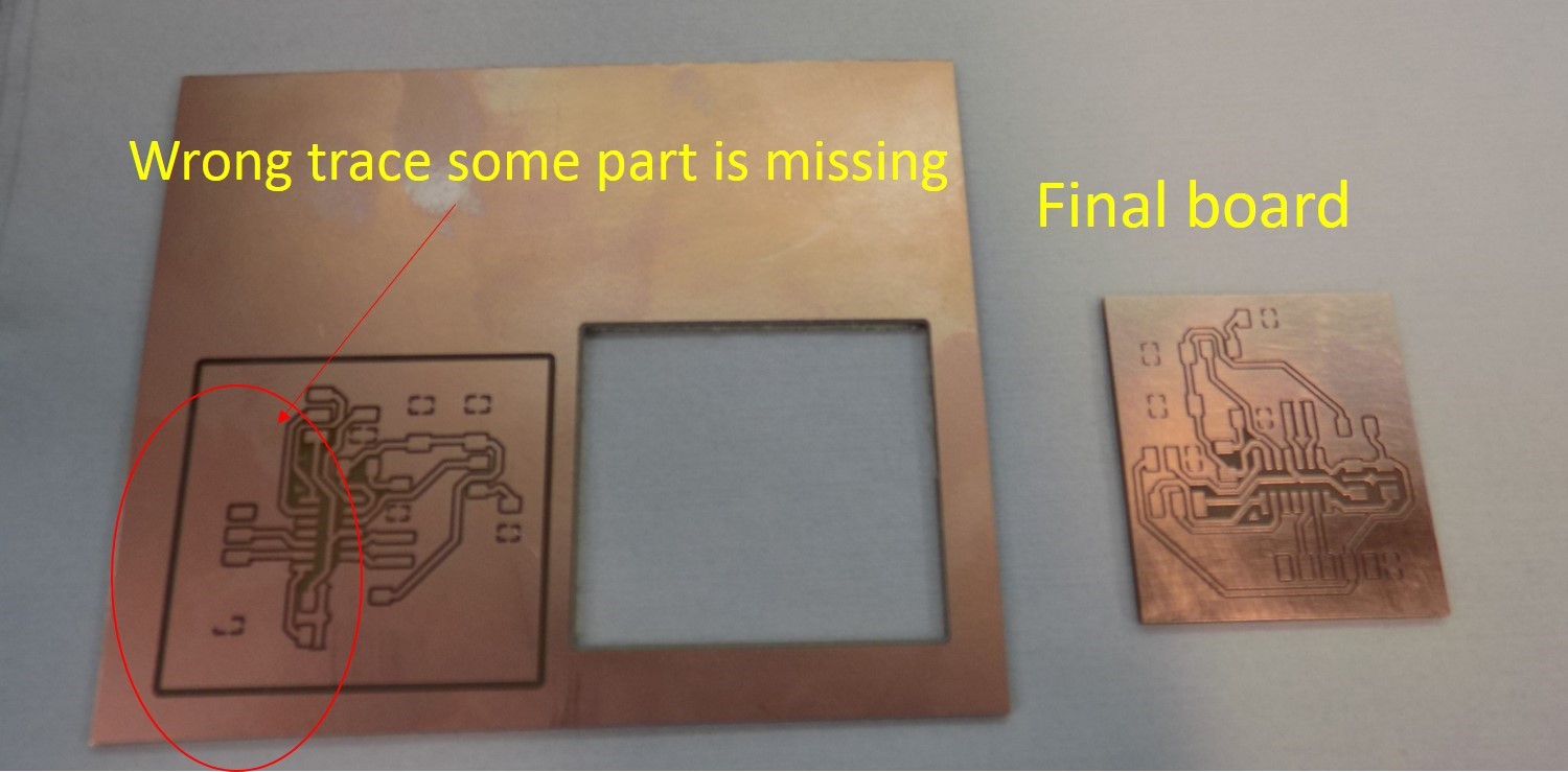
Calculation of milling done with FabLAb mod program same as that of week05 assignment. I used the mod program to make rml file for trace and cut. For this board, I use V-type milling bit with a tool diameter of 0.2-0.5 mm and cut depth of 0.1036 mm and make rml file. Which should not trace properly, see the uncompleted board in the below figure. Then I change cutting depth in the mod to 0.1056 mm and make new rml file for calibrating the trace for V bit. Which is recommended by our local instructors. See the final board in the below figure
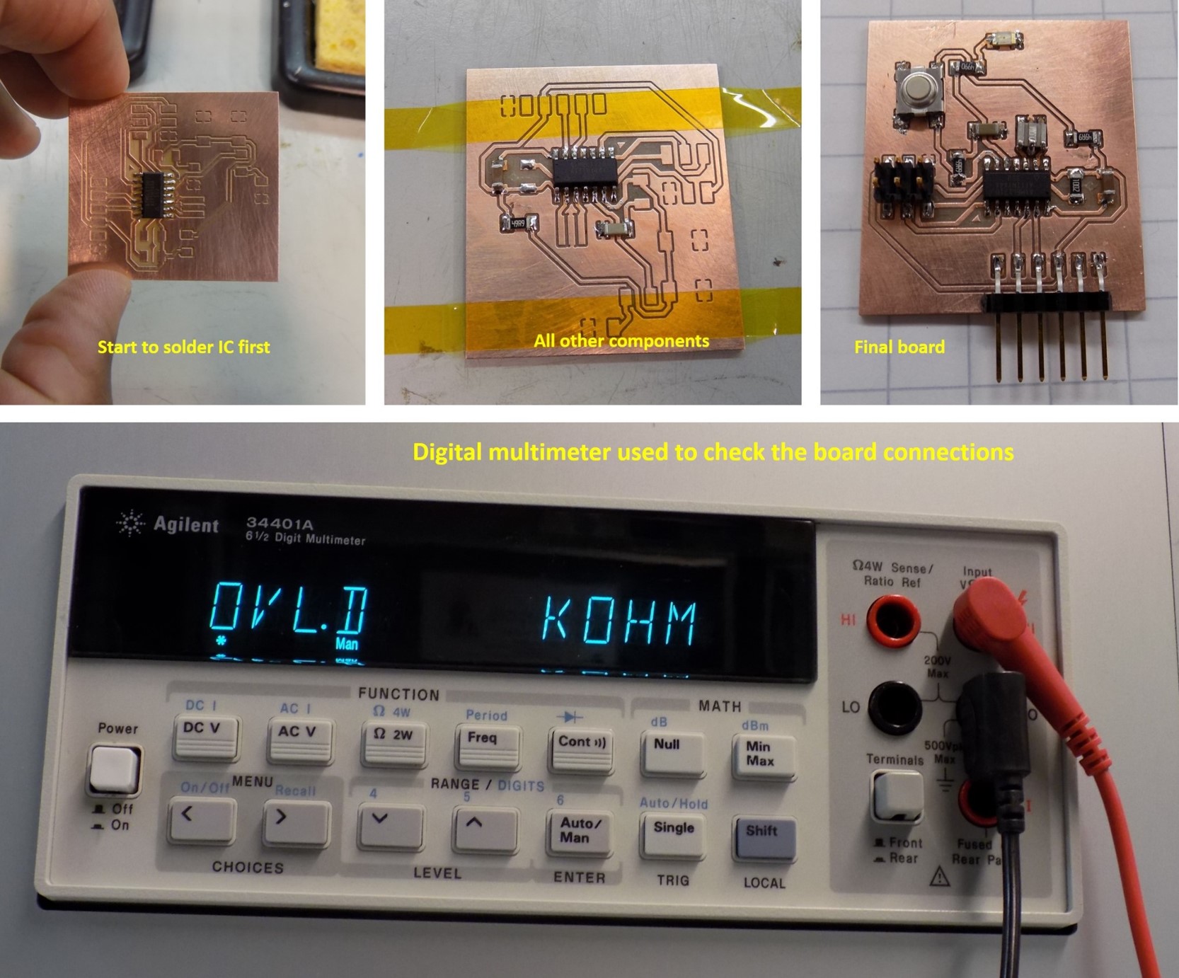
After milling the board start to collect all the component based on my design recommendation and solder the board. See the Week 5-Electronic Production See the figure below,
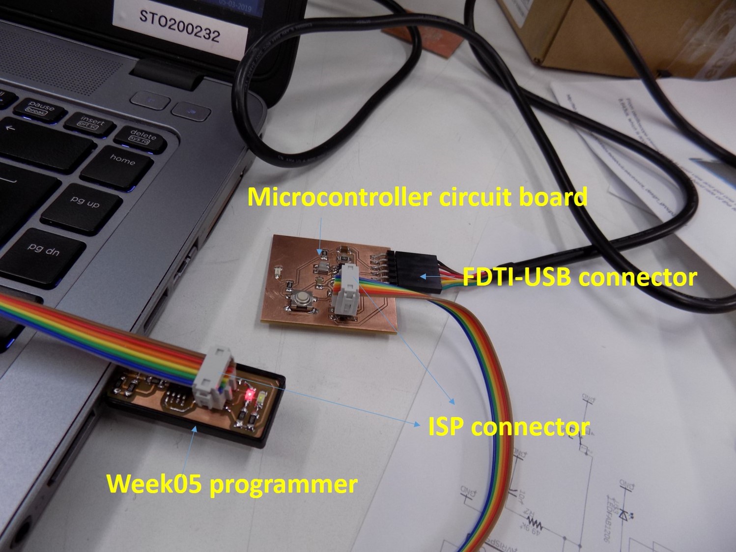
Next step is to programme of my developed board. I used USB/FTDI cable to connect the new board and ISP cable between the boards. Double check the orientation of the cable between the boards. This is a really important part, this may cause damage to your board. So clearly check the board before connecting with ISP. See the figure below for the connections.
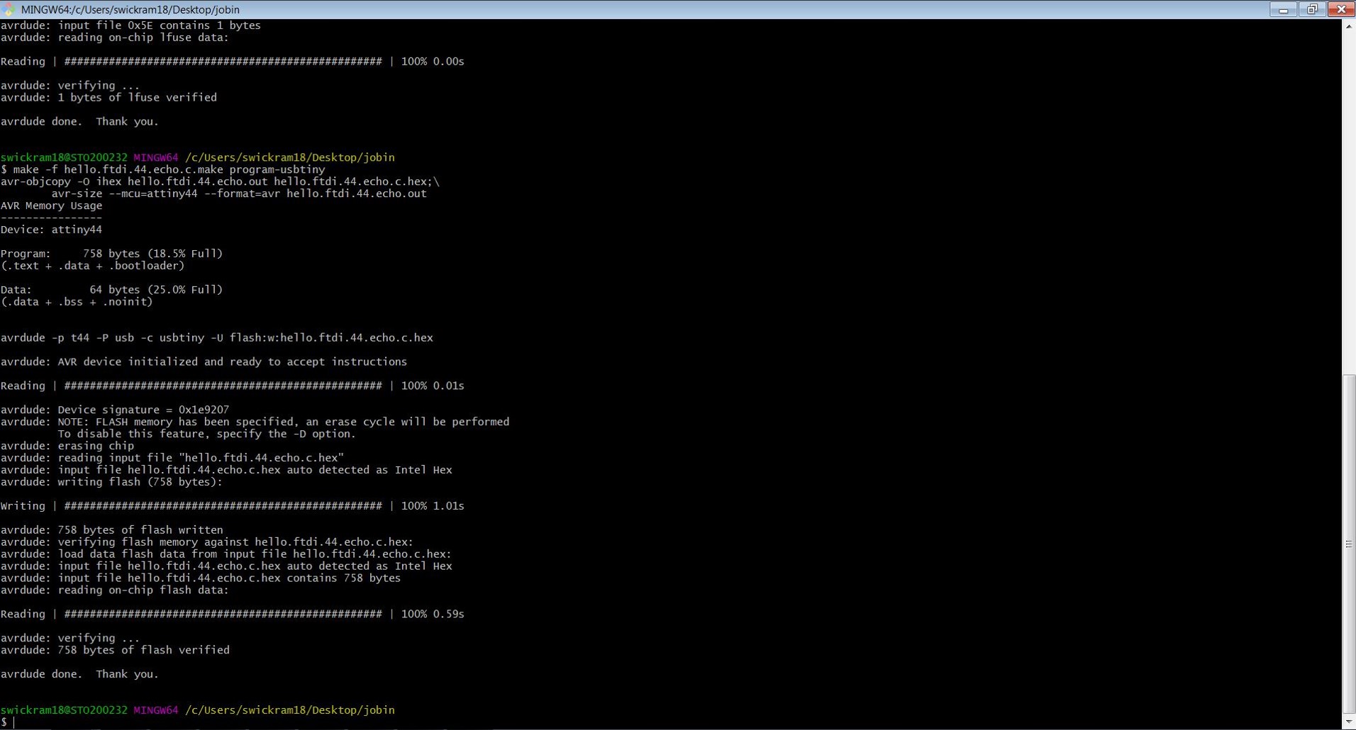
Next step, I need to make a .hex file for flashing, So I downloaded the recommended code and make files and run the command–make –f hello.ftdi.44.echo.c.make—
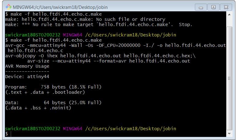
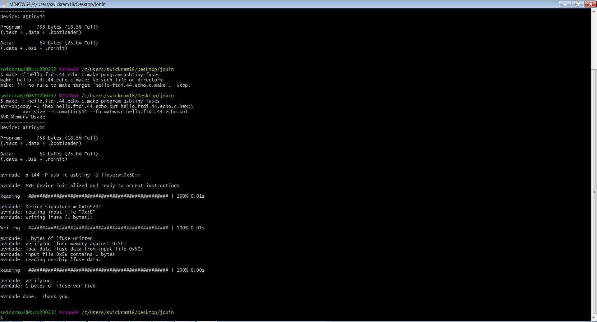
Followed by setting fuses to make the board ready with the command: –make –f hello.ftdi.44.echo.c.make program-usbtiny-fuses—
Finally flashing the developed microcontroller with the command: –make –f hello.ftdi.44.echo.c.make program-usbtiny—
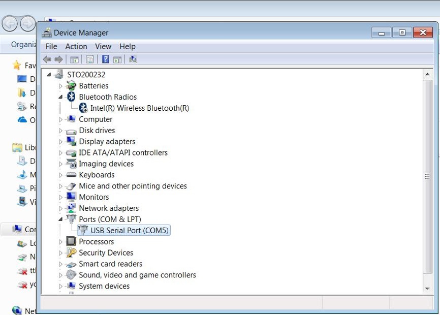
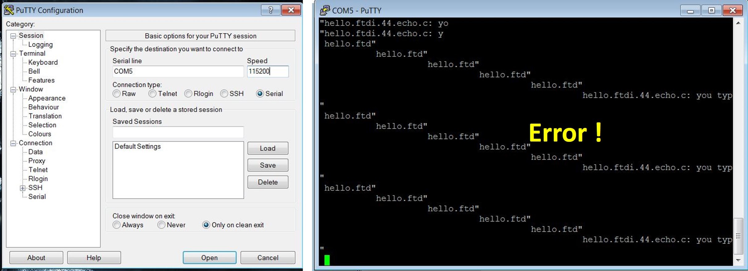
Next step is to test the part. Remove my programmer and left the hello world board attached to USB port. Checking which COM port it was attached. Install putty for control the COM port and see the controller work.
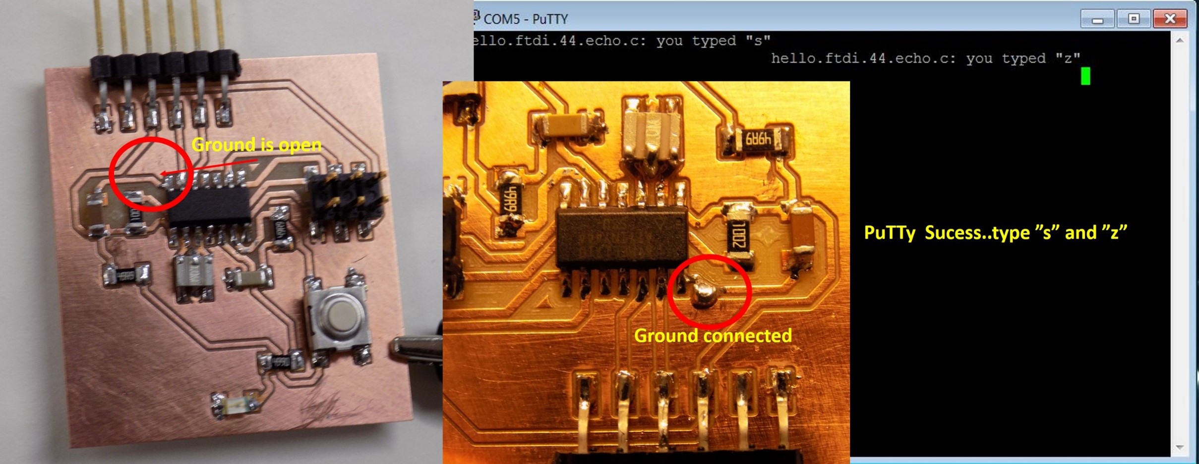
Next step using putty to connect COM5 with 115200 speed. Unfortunately, putty window hanged and does not have any information typed. Some error occurred. Local instructor Antti help me to rectify the problem. IC ground is not connected properly. Then solder it to the nearest ground which is less than 1 mm apart, and it is easy to connect. See the figure below,
After soldering ground, it starts to work properly. I succeed with Hellow world microcontroller programming module. See the below figure with the corrected board and Putty working by type letter “s” and “z” in the keyboard which is shown in Putty. See the figure below.
Group Project
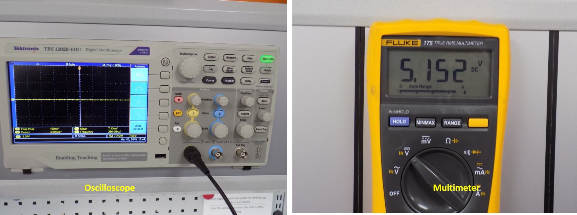
My group member is Yasir Shafiullah and Sahan Sandeepa Wickramaarachchi. Group work for this week was using test equipment in the Fab Lab Oulu in order to test ours on microcontroller circuit board. We had tested our board using multimeter individually first beforehand. Hence, we use one common board to test for measuring the signal using an oscilloscope. See figures of the instruments used for checking the developed board
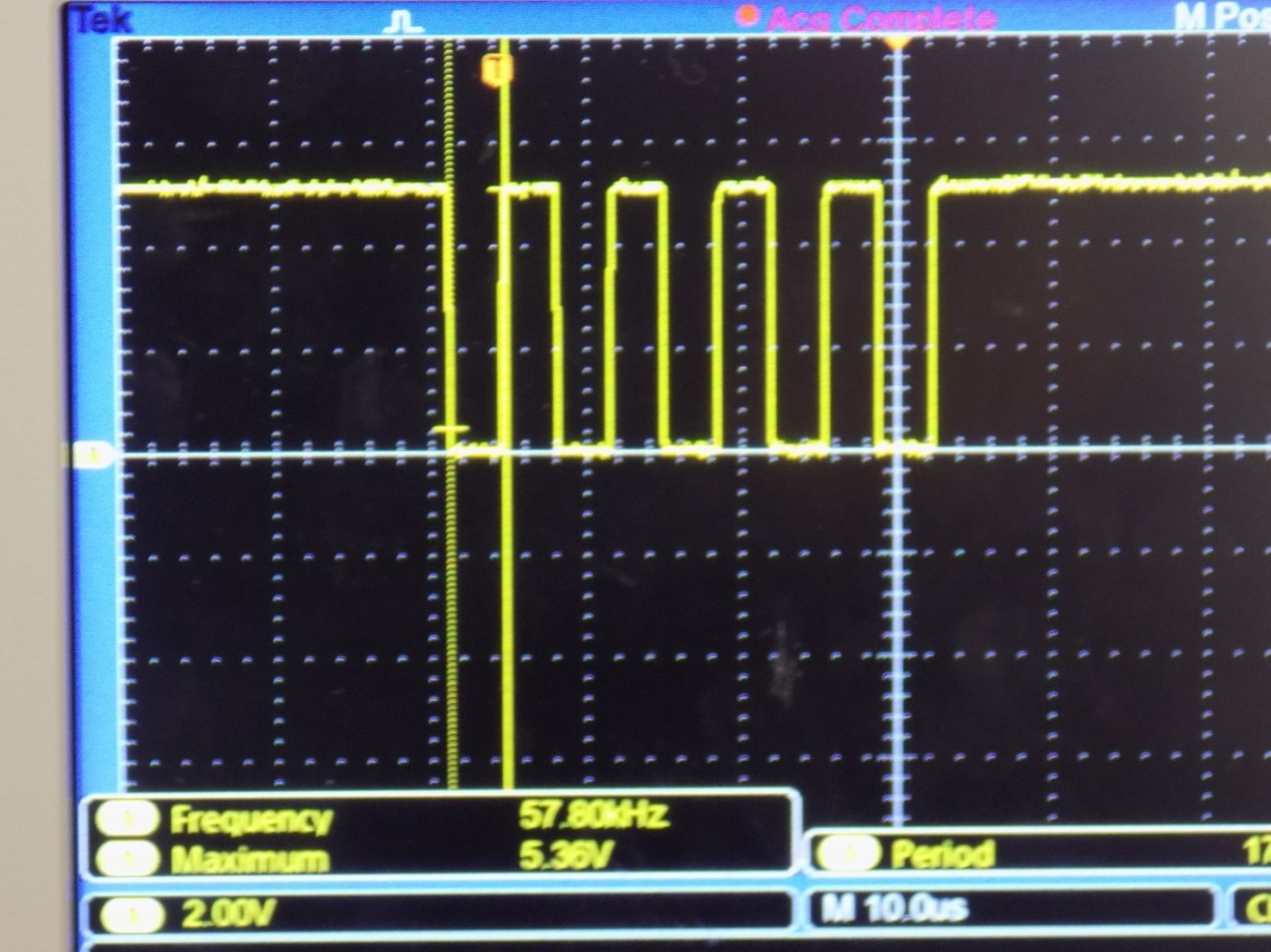
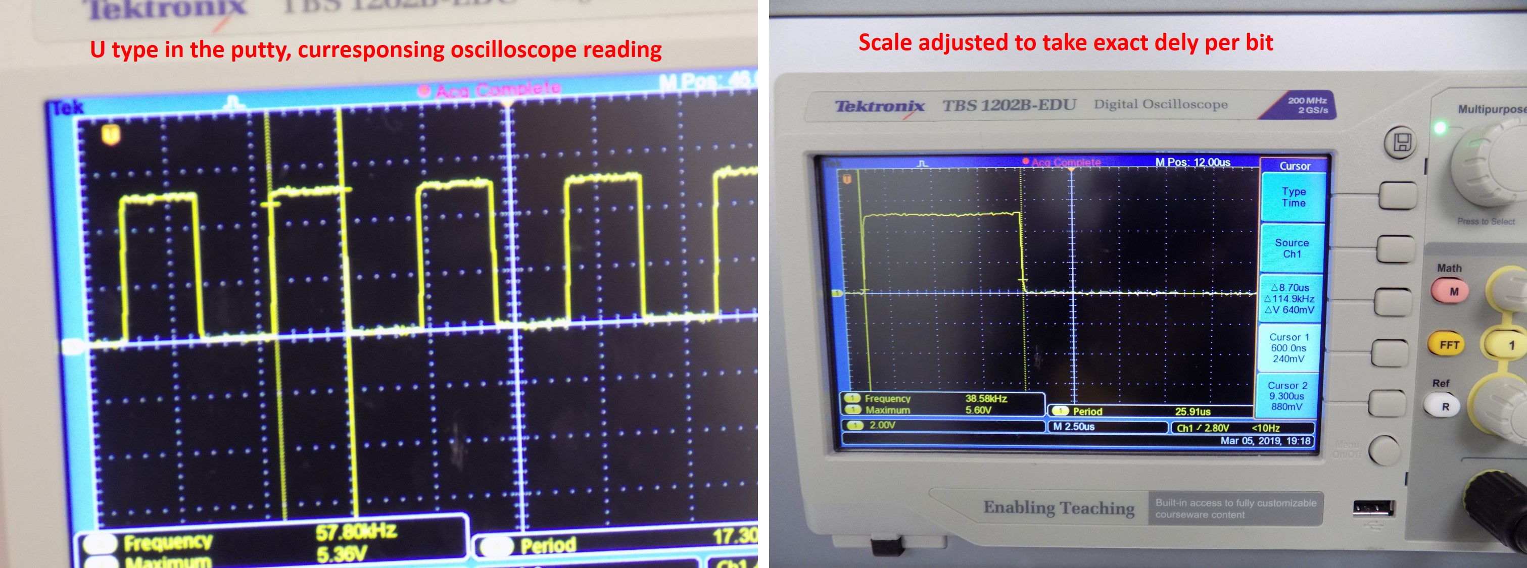
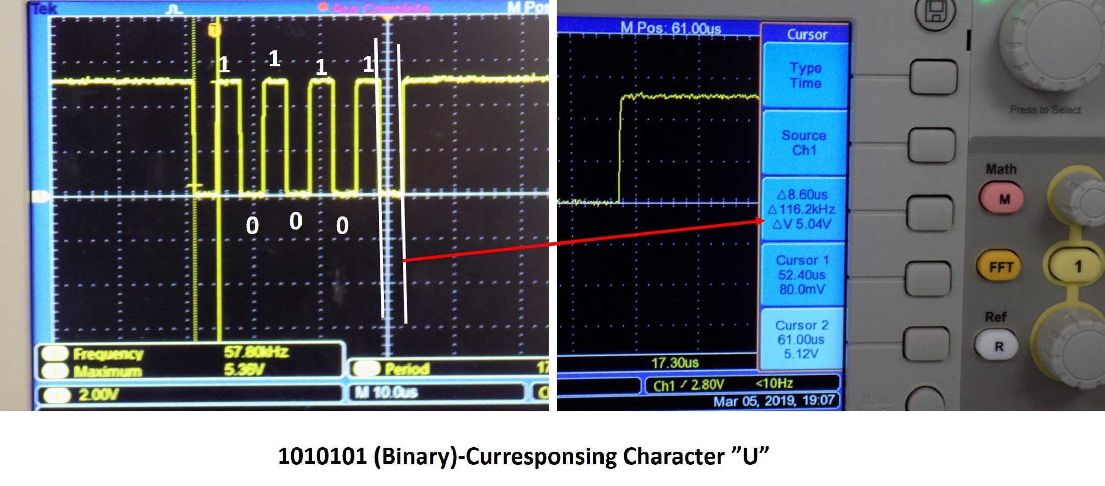
We connected the board to an oscilloscope with black wire is ground and red one to 4th pin that is VCC and type first capital letter U and see the corresponding oscilloscope reading in the figure below, COM5 Putty is used to checking the connection to the board and sending data. We are randomly checking some letter in the terminal. In order to interpret the signal we need to remove the least significant bit from the start and the order of the bits are reversed.
COM5 Putty is used to checking the connection to the board and sending data. See the figure below which type a letter A. See the figure below
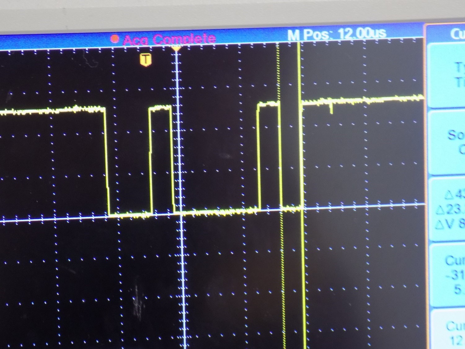
Oscilloscope pressed single to reset view and get one signal. We could see the pulse width is 8 us, which is approximately the inversed rate of the terminal, 115200
Check the ASCII table for binary/hex translation. See the figure below
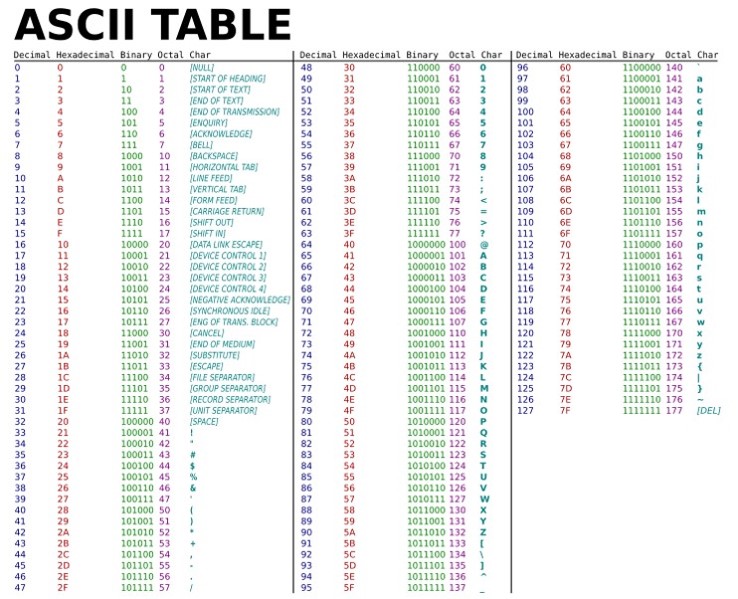
Check the oscilloscope results in comparison with ASCII conversion results
Summary
The week07 assignment consists of the design and fabrication of a microcontroller board and characterises its features and analyses the controller by programming and its evaluation using test equipment. This week, I have learned Eagle design schematic and board design and how to export a png file for board fabrication. Soldering and debugging experiences are improved as compared to the week05 assignment. Learn to measure various electronic test equipments such as the digital multimeter, oscilloscope, supply module and so on.