5. Electronics production
Abstract
A summary of this week assignments is the group assignment and individual making an in-circuit programmer and its results. We started with group assignment to characterise the design rule for your PCB by using milling process. Both assignments are very helpful to learn PCB milling process and in-circuit program production in a systematic manner.
Group Assignment
Characterise the design rule for your PCB production process
My group members are Sahan Sandeepa Wickramaarachchi and Yasir Shafiullah. We used an SRM-20 milling machine. We are decided to use the latest mods server program used for the rml file creation for the milling process. SRM-20 machine support rml file format for milling. Initially, we used an old program for rml file creation, which has an error occurred during the outline cutting. So we decided to use mods which work perfectly for all png file for creating the rml file. The first step to convert linetest_Group.png (5000 dpi) and Linetest interior_Group.png (2500 dpi) converted to an rml file format for milling. The process such as programs-open server program-select SRM-20 PCB-select png file from my PC, i.e., linetest_Group.png (5000 dpi). We have followed by selecting mill trace (1/64) from mod-set PCB default. Then, mod mill raster 2D assign the tool diameter 0.4 mm and cut depth 0.1 mm. Delete the mod WebSocket device and save a new file from the server module by right click option to choose modules-open server-file-save. They are followed by connecting the Roland SRM 20 milling machine mod to newly opened file input in the mod by click both file to connect it. Set x, y, z to 0 in the Roland SRM 20 milling machine mod. Then press calculates in the mill raster 2D mod and weight few seconds waiting time depends on server usage. The process steps are shown in the below screenshot.

Similarly, Linetest interior_Group.png (2500 dpi) converted to rml file. The essential points for notes, Linetest interior_Group.png conversion. Select mill outline (1/32) instead of selecting mill trace (1/64). The tool diameter and cut depth are 0.4 mm and 1 mm.

We are used flat 0.4, 0.5 mm flat bit for testing the PCB production process. The detailed images of the milling and SRM-20 milling machine and line test trace and outline cut file are also shown in the figure below.

Milling machine setting and milling the PCB by the press on the button in the top corner of the machine. In computer open the Vpanel for SRM-20 program controller for setting to initialise the mill bit for cut and trace operation. FR1 PCB sticks with double-sided paper tape as shown in the figure below and placed on to the top of the wooden basement of SRM-20 milling machine. Move the head to origine position, click X/Y-set origin point button, move z-axis close to table, lower the bit, click Z-setting The Vpanel is also shows in the figure below which allow setting to initialise the XYZ position zero before trace and cut operation. Followed by click cut-delete the existing file and add the rml file for milling. Mill bit for trace and outline are different. After milling the trace clean the milling dest using vacuum cleaner and change the mill bit using the align key by carefully hold the mill bit in between two figures without dropping it. Then press output button for start milling. Keep in mind little up after Z zero positioning before output press for starting the milling. See the figures below for more detailed visualisation.

Below figure shows the working sequence on Vpanel SRM-20 milling machine

A standard FR1 PCB is used for this week assignment. The milled group assignment PCB board are shown in the below figure.

It is found that the smallest mill diameter of 0.4 mm can mill 0.001 mm thicker lines. Hence it is summaries that smaller the mill diameter good for file line milling.
Individual Assignment
making an in-circuit programmer
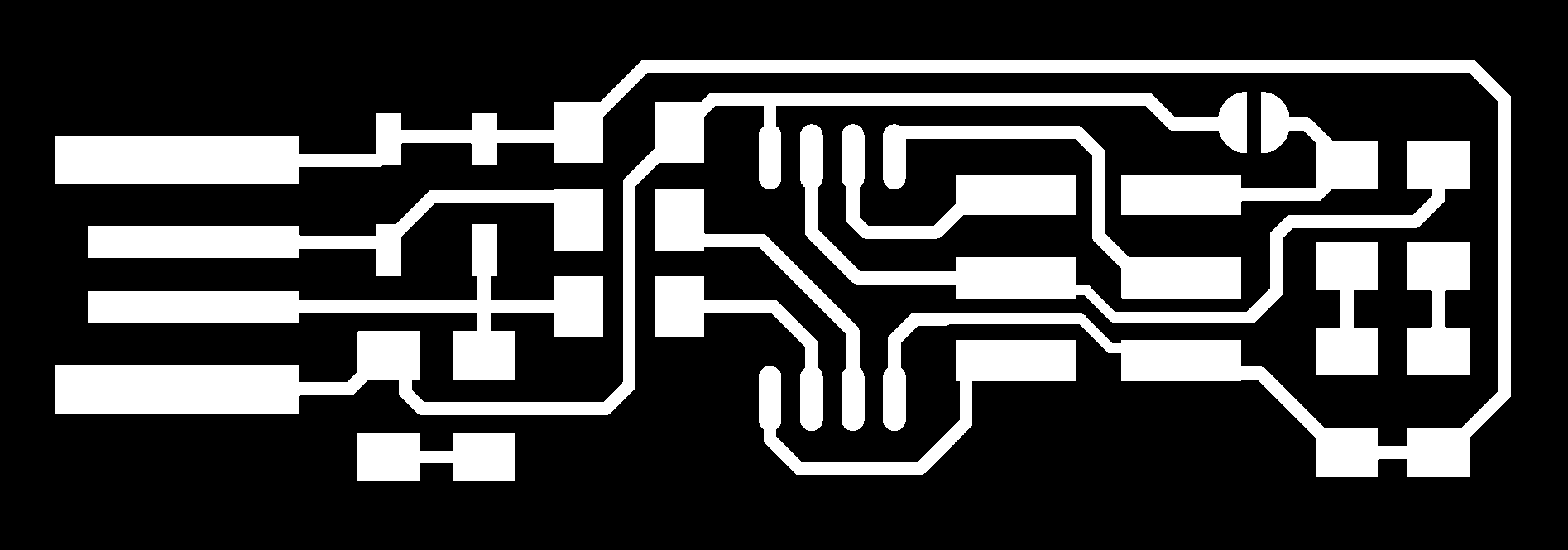
For the individual assignment, I followed documentation by Brian Documentation. PCB fabrication, I downloaded Traces 1000 dpi png file and Outline Cut 1000 dpi png file. Convert the rml file based on the mod program explained in the group assignment. I used flat mill bit 0.4 mm (tool diameter) and 0.1 mm (cut depth for trace). For cutting the outline, I used 1 mm mill bit, and 0.6 mm cut depth per one mill and step down to 3 to 4. PCB mill bit images and trace and cut PCB are shown in the figure below.

Below figure shows the PCB that I developed for the programmer after cleaning with isopropyl alcohol and aluminium fibre sponge for soldering. I have used the following tools for soldering and test fabrication. I have collected all the component which is explained in the Brian documentation, which is shown in the below figure.

The final fabricated in-circuit programmer with different component soldering steps are shown in the below figure based on Brian’s component layout.

The next step is to check the soldering by a microscope for all connections. Followed by check with a multimeter for continuity test before going for the program the chip. When I am checking with the continuity test by VCC and GND, I found that instead of a green LED, I have connected the RED LED. I decided to desolder it and replace the RED LED with a green one in the same place. I followed Brian’s instruction for software installation,I install the following software (see below) to FabLab laptop using Windows 10 platform.
After installation, I updated the path followed by checking the installation and update through the git bash command window. First, check the ‘make -v’ I receive the ‘GNU Make 3.81Copyright (C) 2006 Free Software Foundation, Inc.’. See the following screenshot which represents the installation validation, followed by check avr-gcc and avrdude command in the git bash command window to check the updation of installation files. avrdude checking by connect the programmer to a USB port and type in git bash ‘avrdude -c usbtiny -p t45’and press enter. See the screenshot for more detailed information.

Next step is to build the firmware, I download the firmware source code and extract the zip file to PC. Open the git bash terminal and cd into source code directory and make. This start to create fts_firmware.hex file. This build hex file will get programmed onto ATtiny45. See the screenshots below for more understanding the steps.

The final step is to plug the board into USB port using USB extension cable through a programmed board first and it turn on the RED LED. Connected programmer to the ISP header on to my own board and Run make flash command in got bash command window. I recieved error message which is given in the screen short below. I continously check and replace chip and change resistor 4993 to 4990. Still I am getting the error message not able to program my board. I am planing to make a new board for sort out the problem. Also checking with instructors for correcting the error in the existing board. See the screen short and photos of my board which is connected to ISP header for programing.

Flash error on my board shown below.

I double and triple check the board. Finally, I undestant that the problem. I dont connect my programmer to USB port for power my programmer. Meanwhile, I made another programmer now both programmer work. The programming sequences are shown below,
I access the dowloaded code fts_firmware_bdm_v1 in git bash
Run make

Run make flash

Run make fuses

Testing the board

Yes. it works! Finally, I done one more command Run make rstdisbl. Then I remove my programmer and then desolder the bridge connection in the programmer. See the final figure below,

Summary
This week assignment is the group assignment and individual making an in-circuit programmer and its results. Started with group assignment to characterise the design rule for your PCB by using milling process. Both assignments are very helpful to learn PCB milling process and in-circuit program production in a systematic manner.