7. Electronics design
Eagle
The exercise this week is to design our own version of the “hello world” board, then to upgrade it to include two new components, and finally to build and test it.
Workflow with Eagle
First step was to add the “fab” library, which contains all of the components available in the standard fab inventory. This is done quickly and easily. The library is available on the class page. The xml file in that link is already properly formatted. The .xml extension is removed and the file is saved into the /eagle/lbr directory. Then in Eagle:Library:Library Manager, the fab library is added using the Browse button.
The rest of the Eagle process is as follows:
Create a new project
Use File:New. This creates a pair of windows, one for the schematic (white) and the other for the board (black). All circuit editing is done in the schematic window. The board window is used to place the element around the board and link them with the traces (called nets).
Add component
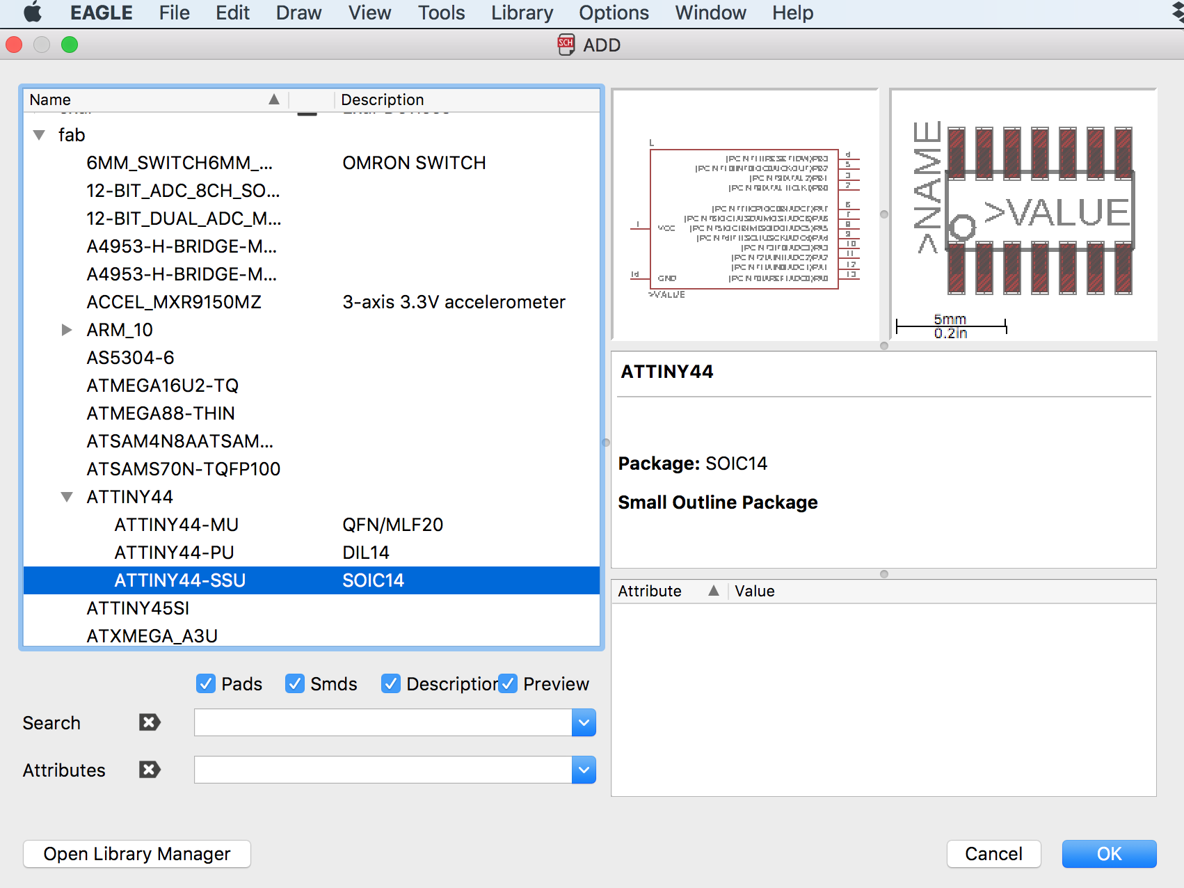
Clicking on the  button brings up the library window. There is a search function, but the fab library is small enough that individual components can be found simply by scrolling. Here the AtTiny44 with SOIC14 packaging is highlighted.
Once the elements are placed on the schematic, they can be arranged using the move function (![]() ). Idea is to arrange the elements so that the connections are clear and don’t cross too much.
). Idea is to arrange the elements so that the connections are clear and don’t cross too much.
Make connections
The various elements are then linked using the “net” tool ( ). Each net can (and should, where useful) be given a name - this is done by right-clicking on the net while in “net” mode, and selecting “Name” from the pop-up menu. The nice thing about this feature is that all named parts of the net are then connected in the background, even if not represented as such in the schematic window. The schematic can be done either by connecting every pin using the net tool, or using labels. Labels are added using the “label” tool (
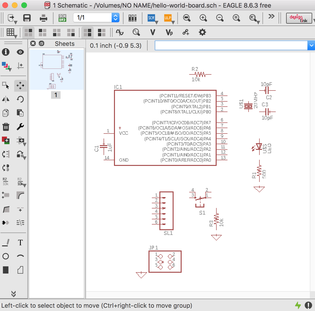
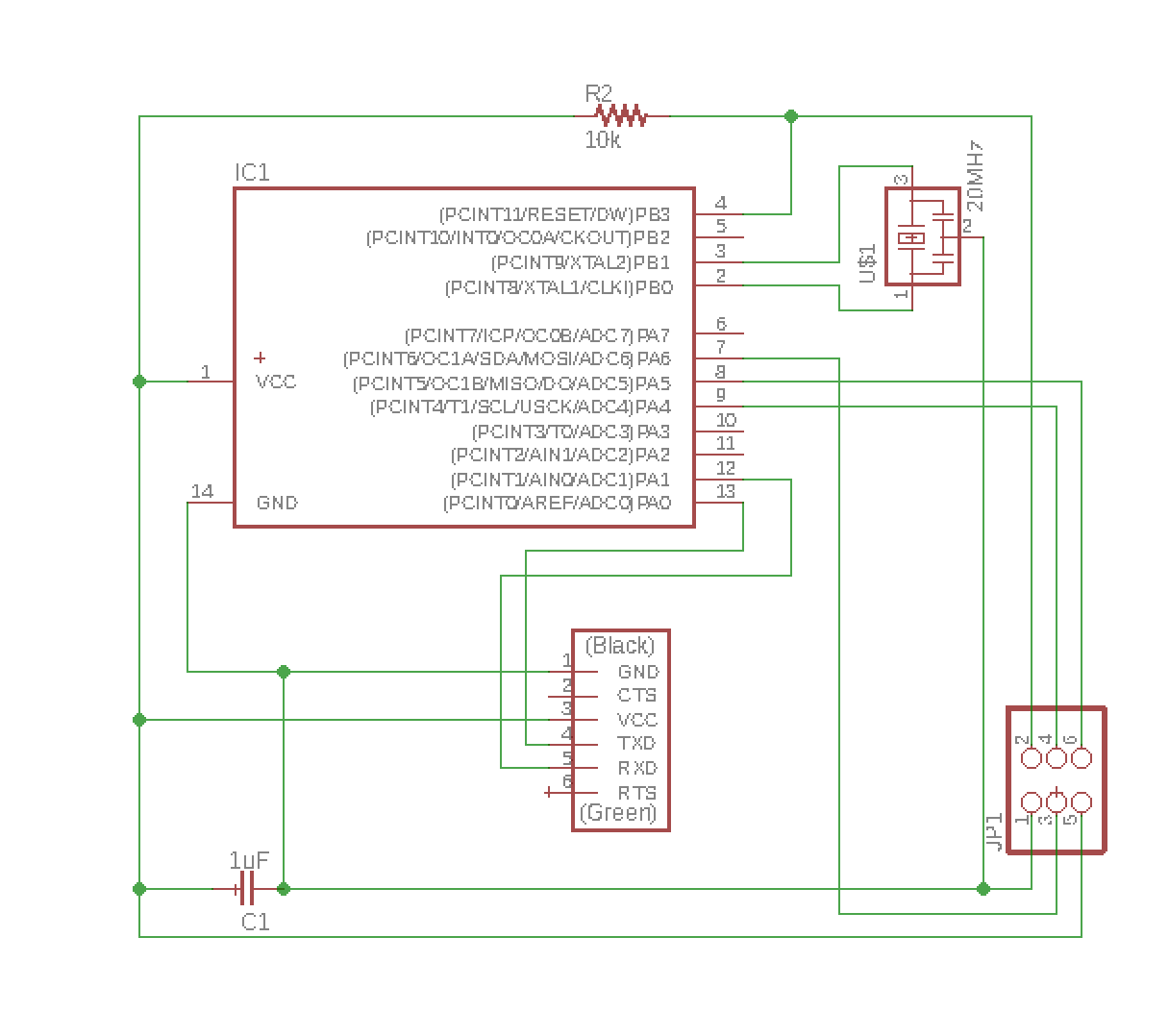
 ). A completely labelled schematic is shown below:
Route the board
Once the schematic is set, then one moves to the board layout itself. The  button can be used to change windows. The elements are all placed willy-nilly in the bottom left corner of the window. They need to be arranged on the board itself. Easiest is to place them more or less correspondingly to the schematic to begin with. They will need to be rotated and moved around as the wiring starts in order to keep connections short and so as not to cross them.
Settings
Before getting too excited about routing the components, it’s important to set the minimum trace width that the mill can cut. I can’t remember right now how we set that, but I’ll dig it up once the rest of this report is finished.
Ground layer
Once the initial wiring is done, it’s time to create the ground layer. Use the polygon tool  to surround the board elements. Clicking on the ratsnest
  tool will fill in the ground layer. The final design will require a bit more shifting of elements and probably some rerouting of nets to ensure minimum clearances are met, and that all elements remain connected as required.
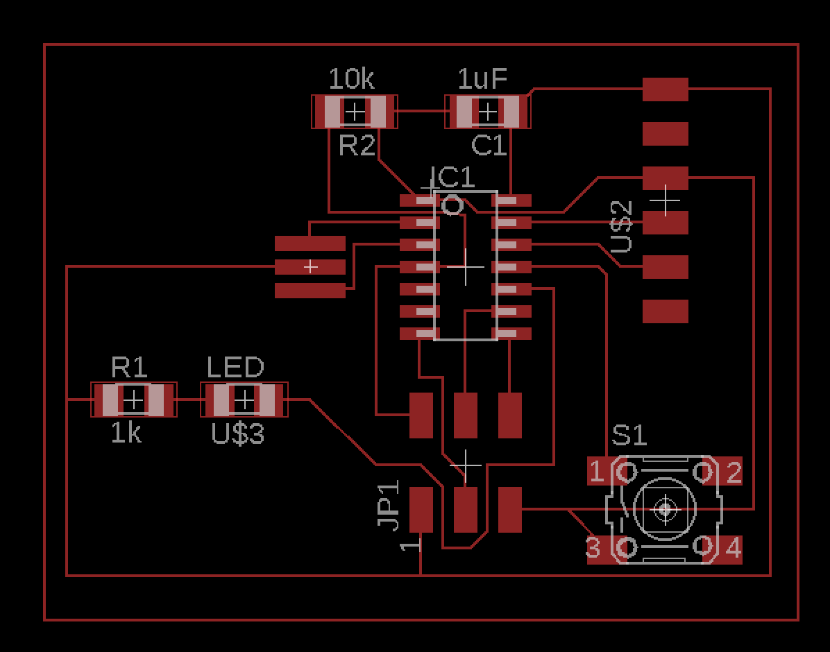
Original Board, Revisited
The original board is shown on the class website here.
The components include an ATtiny44 microcontroller, a 20MHz resonator, a 10k resistor, a 1uF capacitor and two bus connectors. Gathering them into Eagle and arranging them nicely results in the following schematic:
Upgraded Board
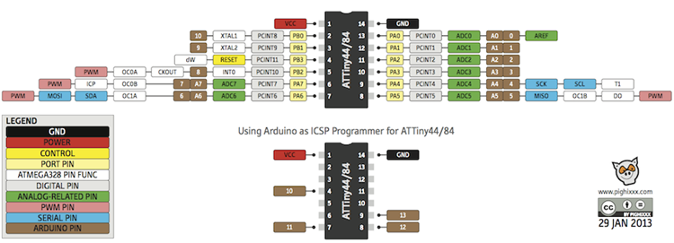
Having recreated the board and in the process learned a bunch of Eagle philosophy, it’s time to design a new board. The process starts with a visit to the device datasheet, which is found here. There is plenty of information available there, but all we need for this particular design project is the artistic rendition of the connections to the chip, generously provided by Alberto Pighi, and reproduced below:
Circuit design
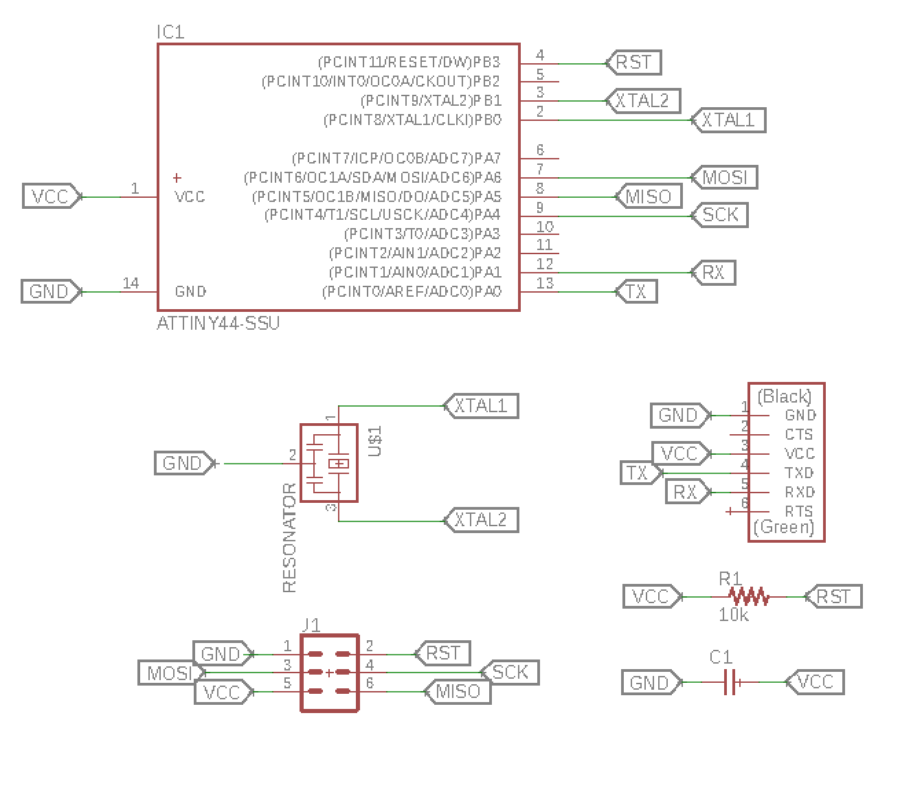
First step in this case is to decide how to use the microprocessor pins. Vcc and GND are obvious. We’re using an external timing crystal, so XTAL1 and XTAL2 are also set for us. There is no built-in networking on this chip, so two lines must be dedicated to serial communication (RX and TX) - easiest just to stick with the example here and use pins 12 & 13. MISO, MOSI, SCK and RESET all have to be made available to the programmer (through the 3x2 connector). When not in use for programming, they can be used for other things as shown in the Alberto’s diagram. In this case, we want to include a switch and flash an LED, so we need one digital input (hi/lo) for the former, and a PWM output for the latter (so that we can flash and/or dim it). For board routing purposes, it was most convenient to use pin 8 for the LED and pin 10 for the switch.
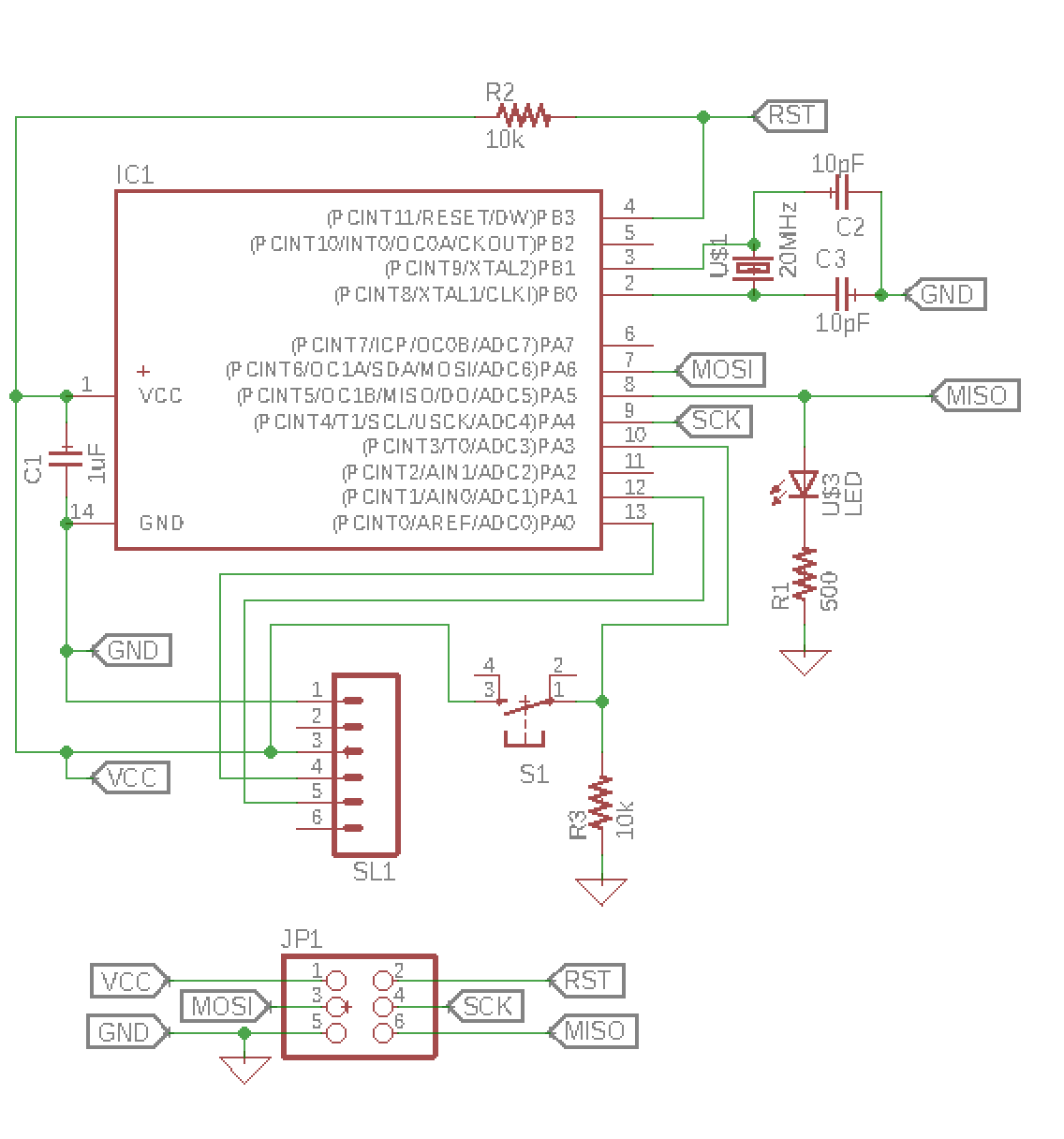
Away from the microprocessor, there were two other decisions to be made. The LED requires a current limiting resistor. As the board runs on 5V Vcc, that’s the level to which the output pin will go. With a 500 Ohm resistor, the LED will see 100mA, which will make it nicely bright. Pin 8 (PA5) was chosen to run it, as this pin is also set up for Pulse Width Modulation (PWM) output, which will make it possible to control the brightness of the LED programmatically.
Button: pulling high/low with anchor. In order to ensure that the pin on the microprocessor sees a distinct HI and LO, both states of the switch have to be connected to the circuit. If the switch were only connected to Vcc to make the HI, then when the switch was open, the pin would “float”. By connecting the pin to GND through a resistor, the voltage is held low when the switch is open. When the switch is closed, then the current flows through from Vcc, and the voltage rises to the HI state.
Header elements. The mechanical connections to the board are important. Because I’m a bit of a clutz, I’d rather have the external connectors able to physically take the hits from plugging cables in and removing them. So I’ve used a 1x6 header set, and drilled holes in the board to transfer the stress to the base of the board, rather than just through the solder joints to the copper layer.
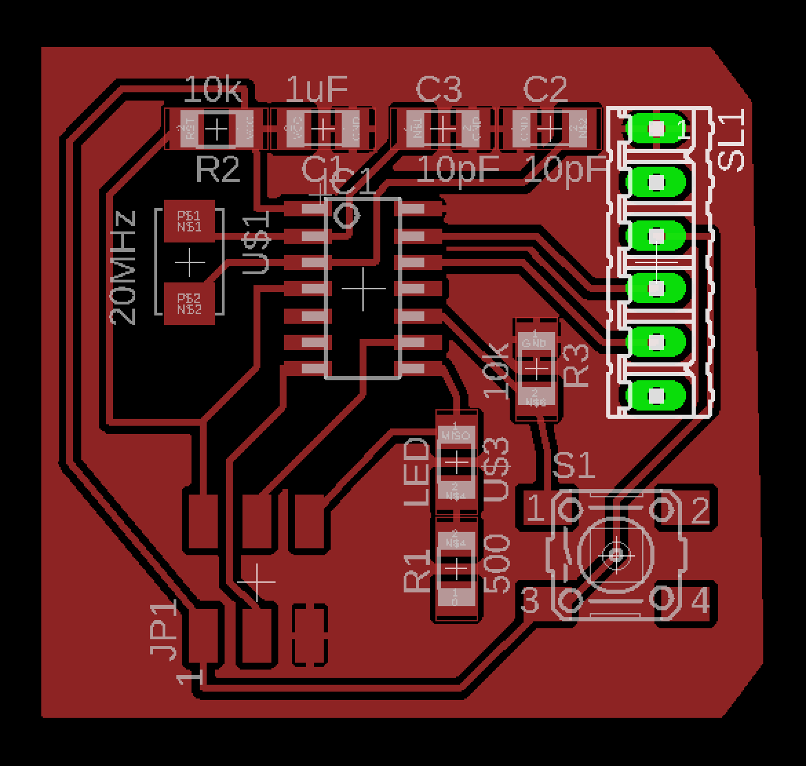
The final design of the circuit was a combination of direct connections and labels.
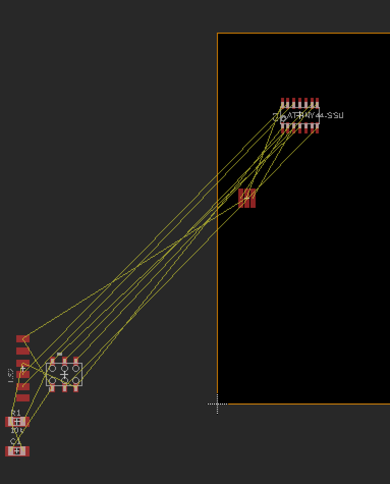
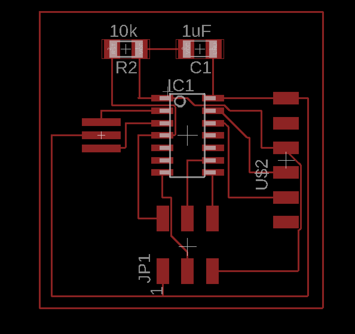
The first draft of the board looked like this:
It quickly became obvious that it wasn’t going to be possible to manufacture this, as the minimum width of the traces meant that they couldn’t be routed between the pads of the chip. It was also inefficient in its use of space. So I shifted things around and rerouted the traces. The final draft of the board looks like this:
Manufacture
In a previous assignment, I learned how to manufacture a board, so I won’t go into detail on the steps involved. Last time, we worked from a preprepared black and white image. This time, the image was to be exported from Eagle. Since I’m working on a Mac, there was one extra step, as the Eagle export function doesn’t scale the image properly. To work around that problem, I exported the schematic and board files to a Windows computer, and reworked them there before exporting them. I’ll come back to this later to describe a consistent workaround for the Mac.
I imported the eagle exports into Gimp, then processed them as before to convert to binary images, then cut out the internal and external graphics to send to the CAM software.
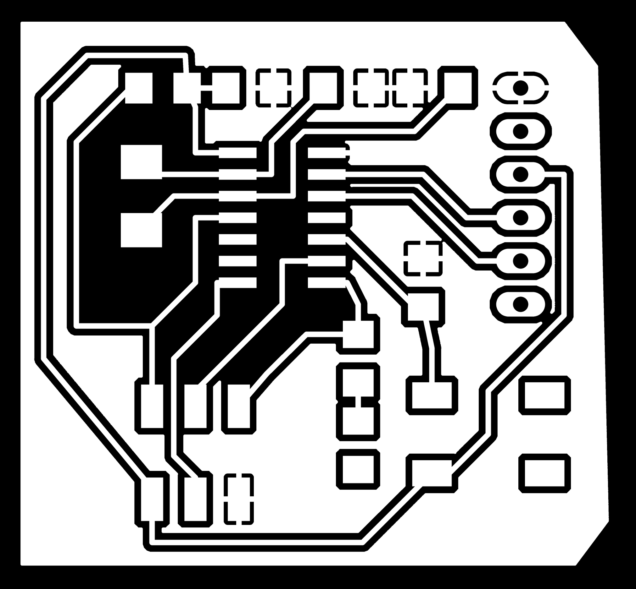
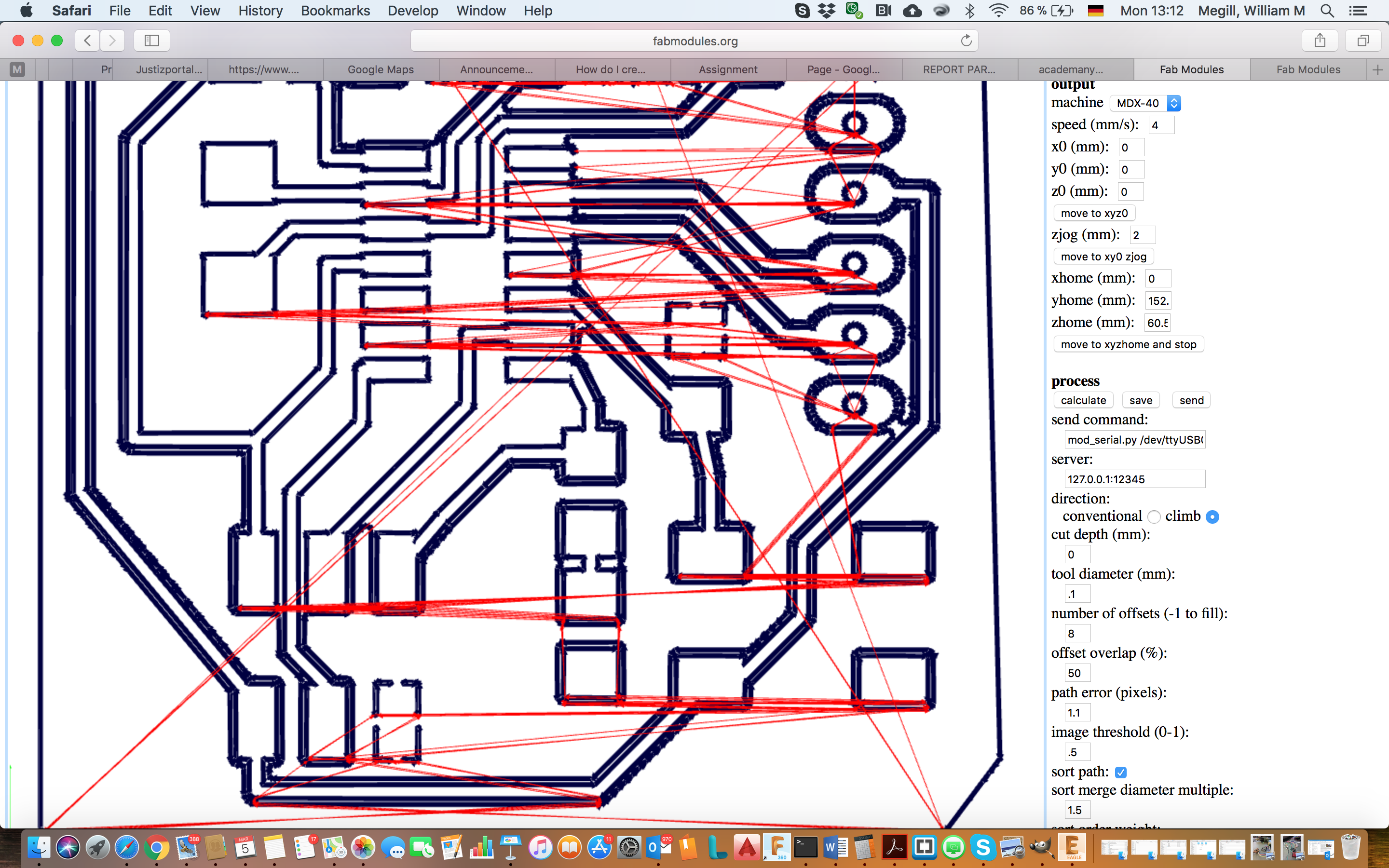
I used fabmodules.org to make CAM instructions, following the same procedures as in the previous assignment. The tool path that was generated for the internal cuts looks like this.
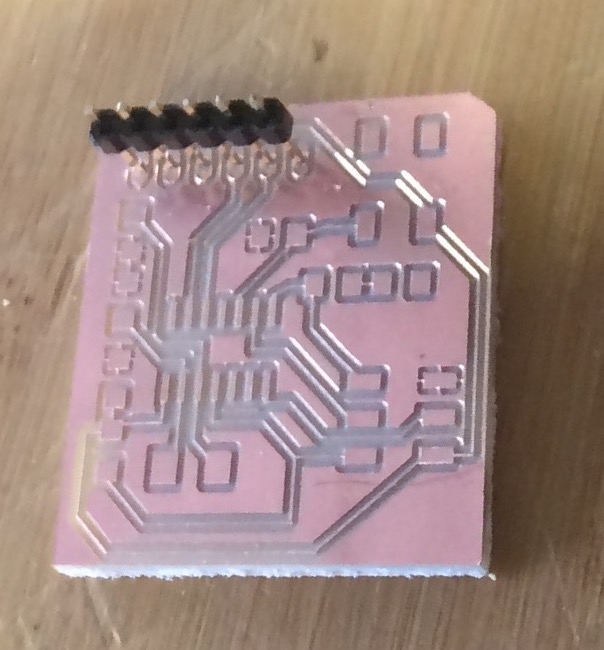
I ran the mill in the usual way. I’ve got to practice some more with the setting of the z-axis. Here I cut too deep, and as a result the traces are very narrow.
Mechanical connections are important!
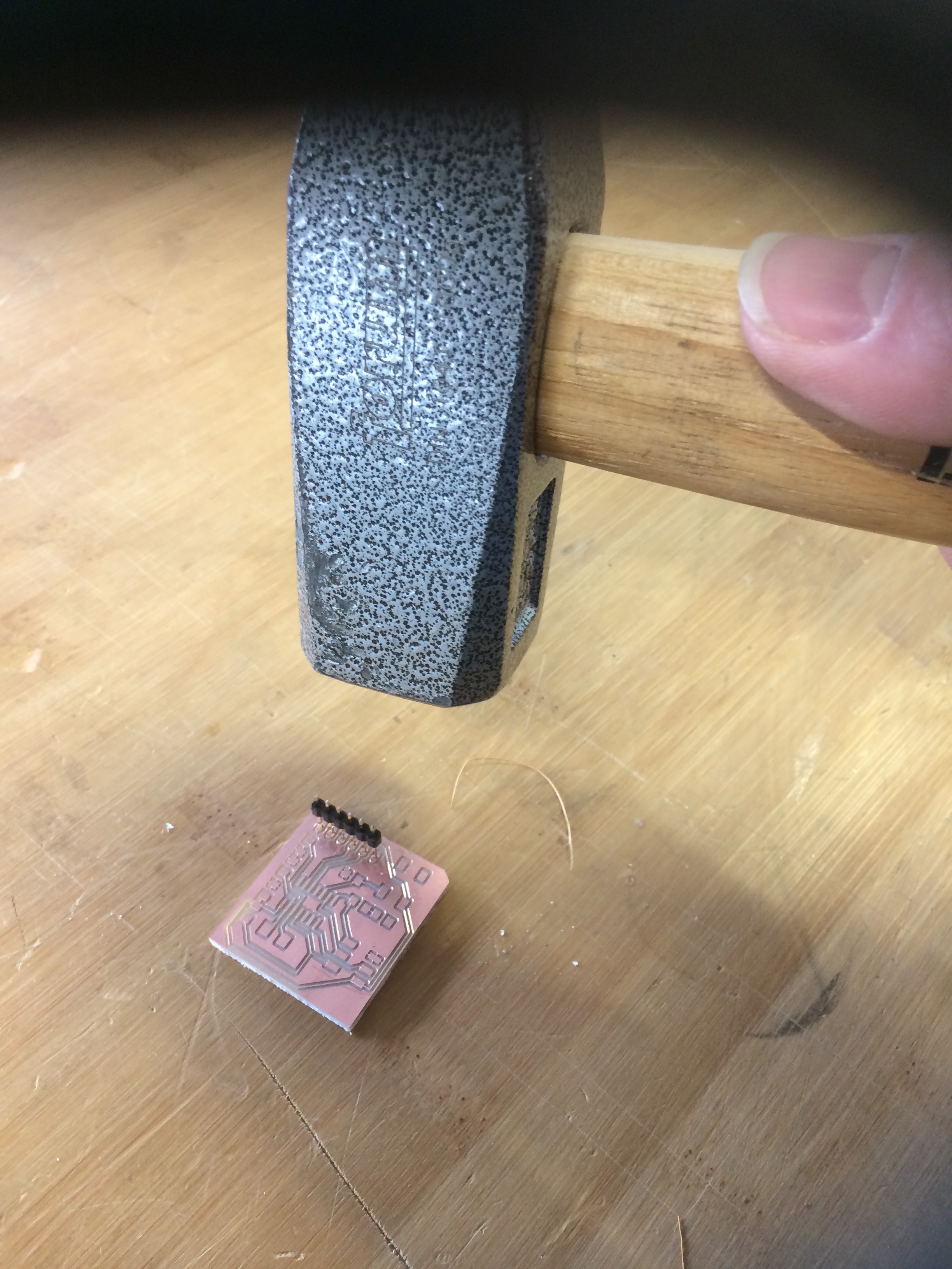
I drilled the holes for the FTDI using a dremel tool mounted in a small drill press. I deliberately cut them too small, so that the torque on the header would be transfered into the base of the board. So to place the pins in the board, I “gently” hammered the square pins into the round holes.
Continuity and Band-Aids
Before carrying on, I tested all of the continuity, focusing in particular on all of the connections where the traces were really narrow. That highlighted a discontinuity in the ground plane, which I fixed with a zero ohm resistor “Band-Aid”.
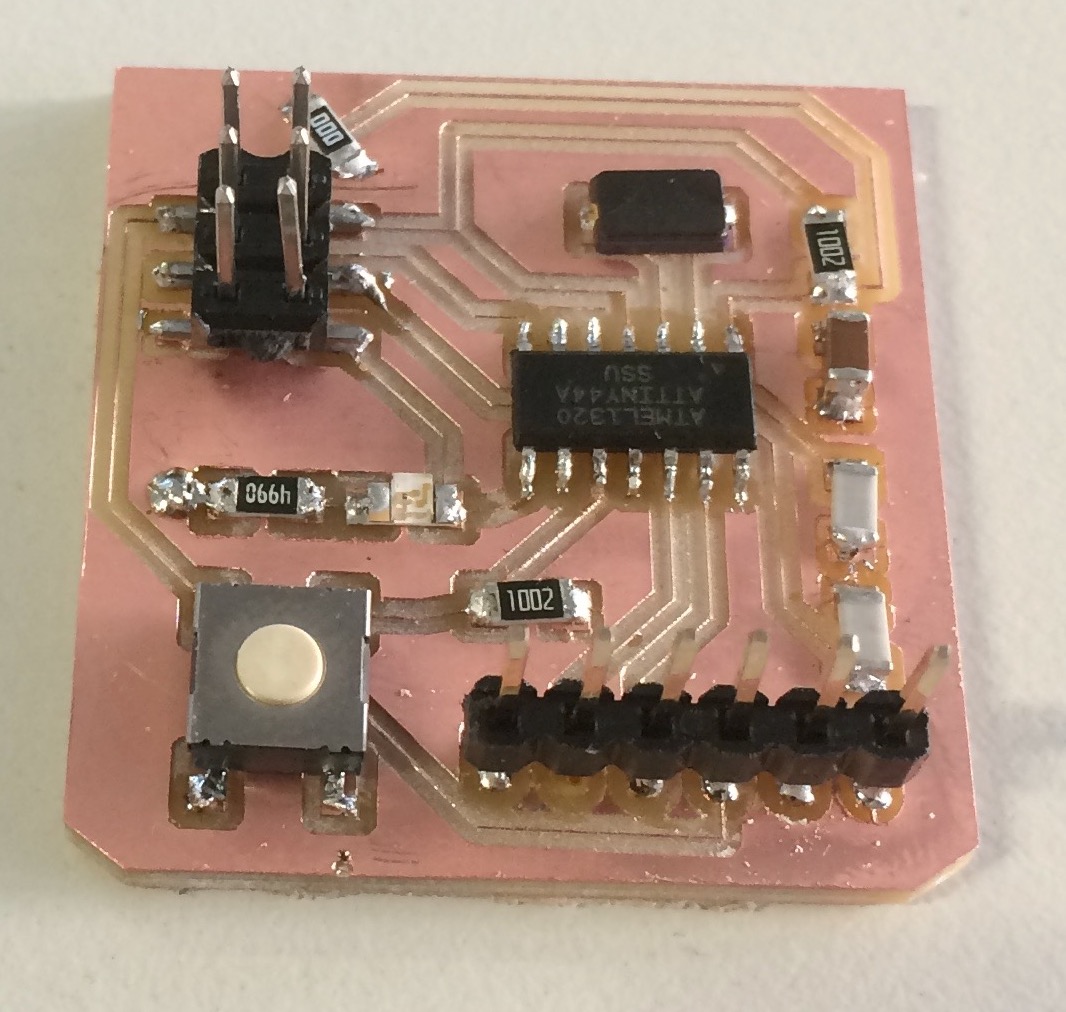
The final board
Soldering went ok, though I did have a few challenges due to the narrow traces. Some of the shininess was difficult to achieve with the lead-free solder I was using. Note also the Band-Aid in the top left corner, behind the 2x3 header.
Programming
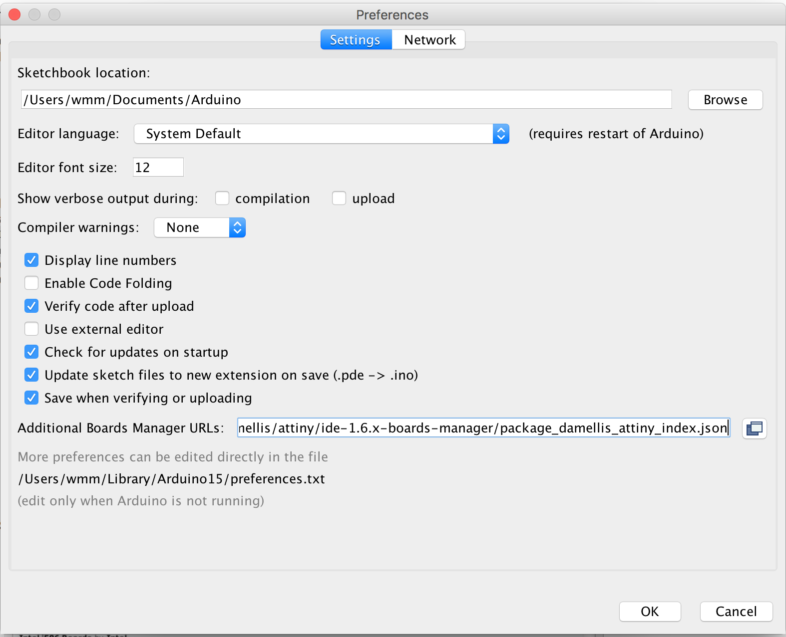
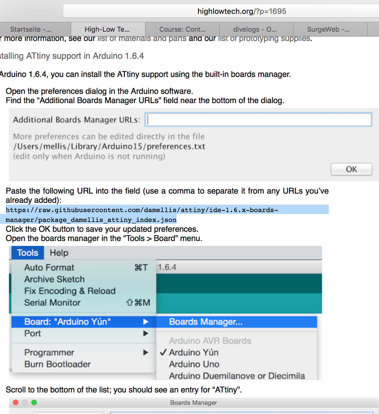
Smoke test: Connect USB/ribbon cable to FTDI connector. Connect to USB hub. Connect 3x2 headers with jumper wires - careful pin-out different. Note pin numbering: top left = 1, then zig-zag across, down. Line HelloWorld FabISP GND Pin 5 Pin 1 VCC Pin 1 Pin 5 MOSI Pin 3 Pin 3 MISO Pin 6 Pin 6 SCK Pin 4 Pin 4 RST Pin 2 Pin 2 Plug FabISP into USB hub. Install latest Arduino IDE 1.8.5 Install ATtiny support - highlowtech.org/?p=1695. Arduino:Preferences:Additional Boards Manager URLs: copy https://raw.githubusercon…
Restart Arduino IDE Arduino:Tools:Board:Boards Manager
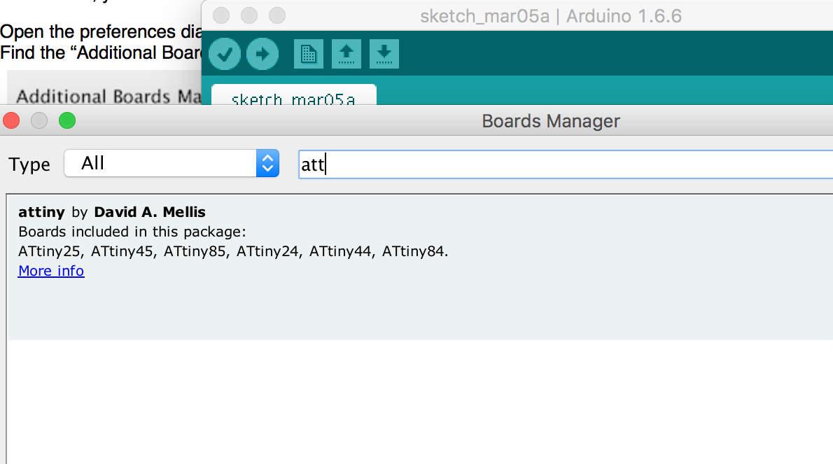
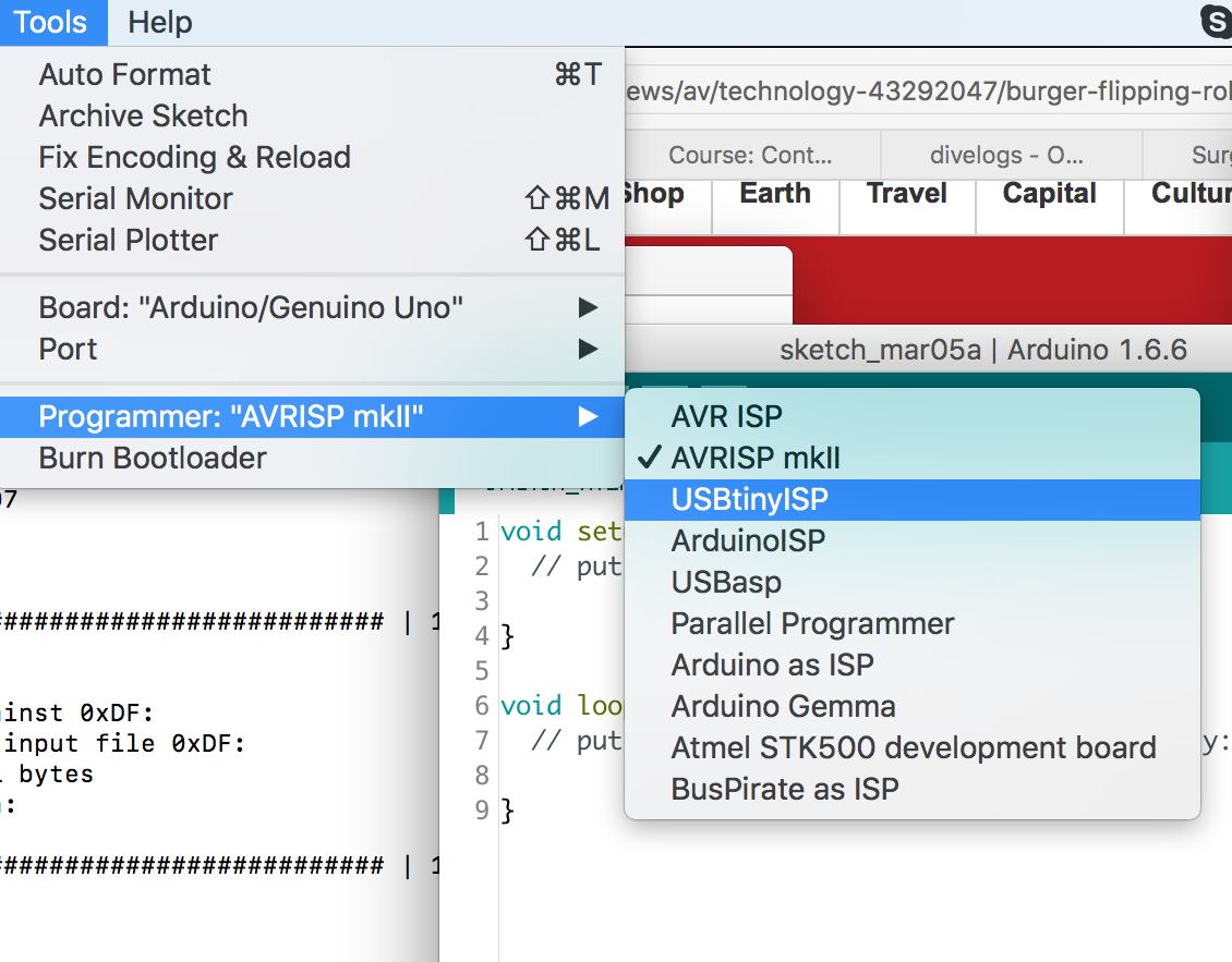
Arduino:Tools:ATtiny44 Arduino:Tools:Processor:ATtiny44 Arduino:Tools:Clock:External 20MHz Arduino:Tools:Programmer:USBTinyISP
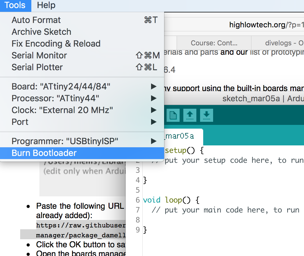
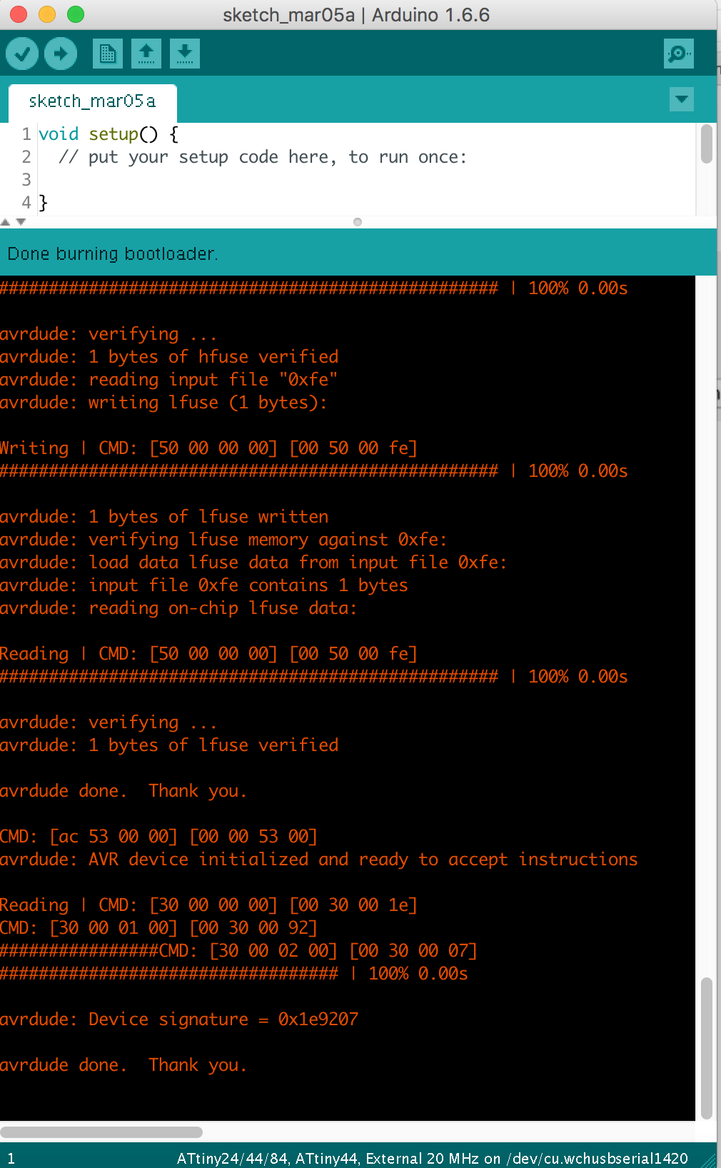
Arduino:Tools:Burn Bootloader
Response file - AOK
Arduino:File:Examples:Blink
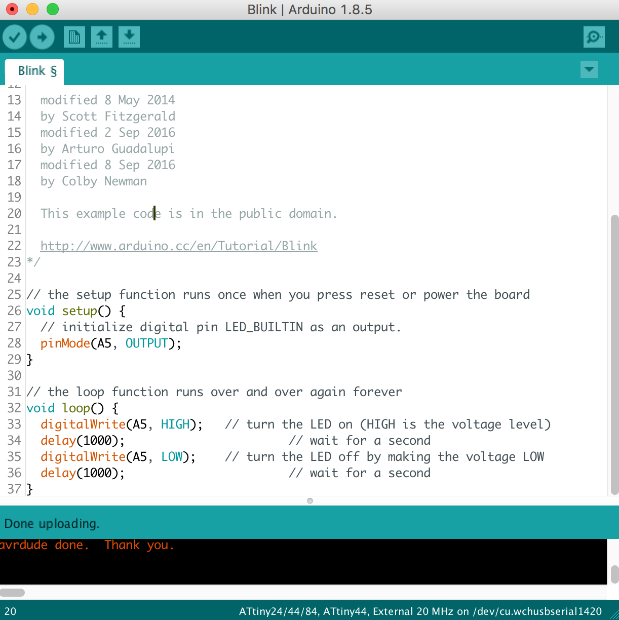
Set port number to “A5” (the output pin I used in the hello world board) Arduino:Sketch:Upload using programmer Picture of success
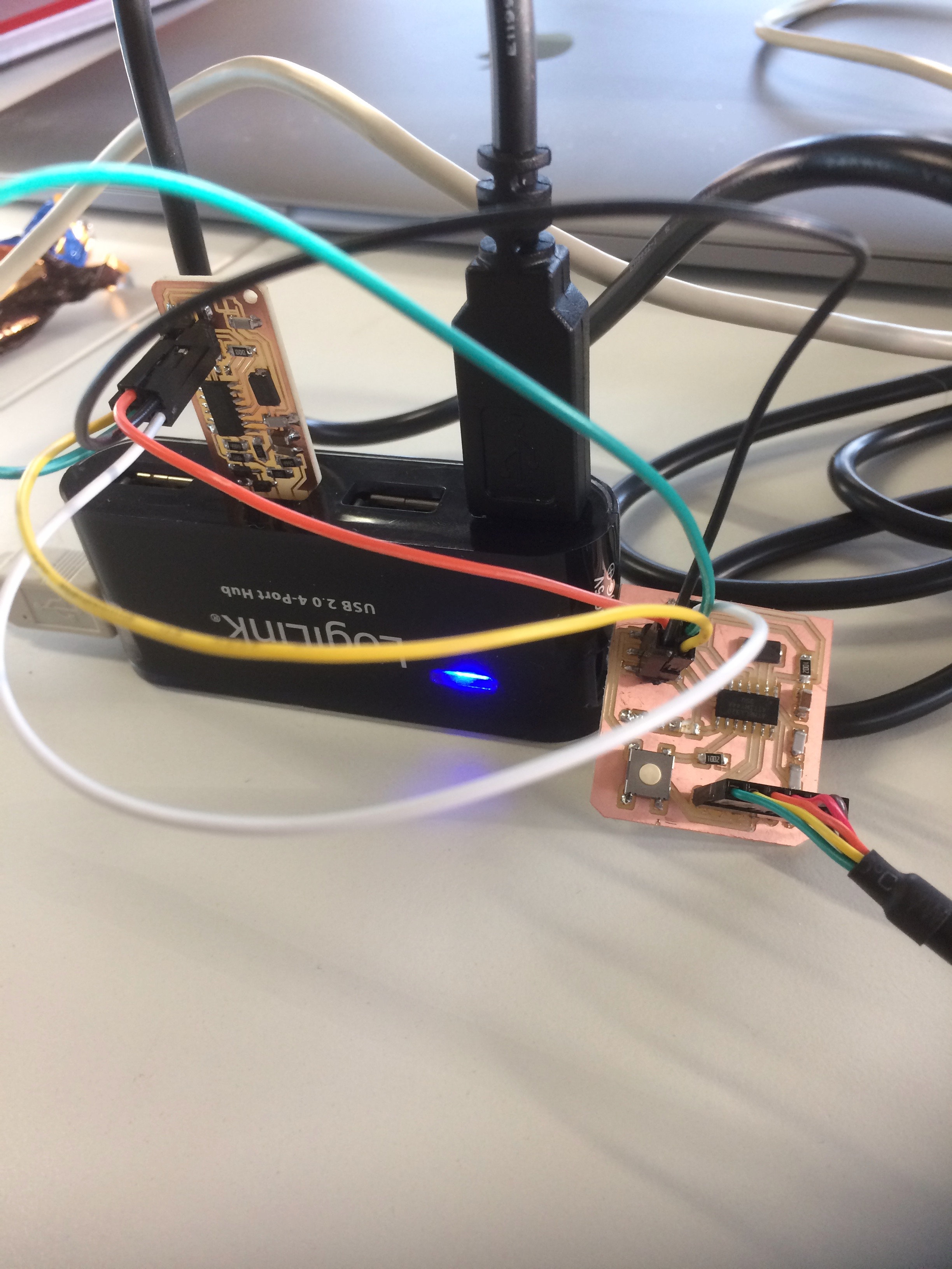
Unplug all wires. Plug back into power, and voila.
Downloads
- Board
- Schematic