|
Assignment 7:electronics production.
In the following weeks we will learn to program our own microprocessor. As a preparation excercise we drew and produced a board with a button and LED. The focus was on learning to work with PCB design programmes so we re-drew an example and added the button and LEDs. These are the steps to follow:
1. draw a schematic of the circuit
2. organize the components on the board
3. create the milling paths and export to .png
4. mill the board
5. solder the components
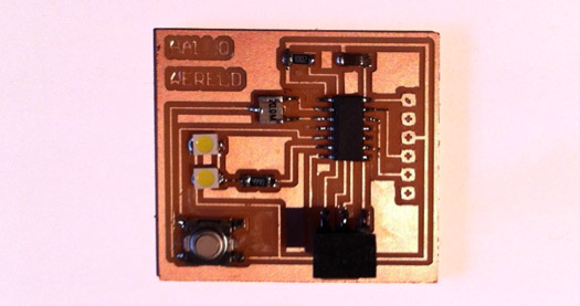
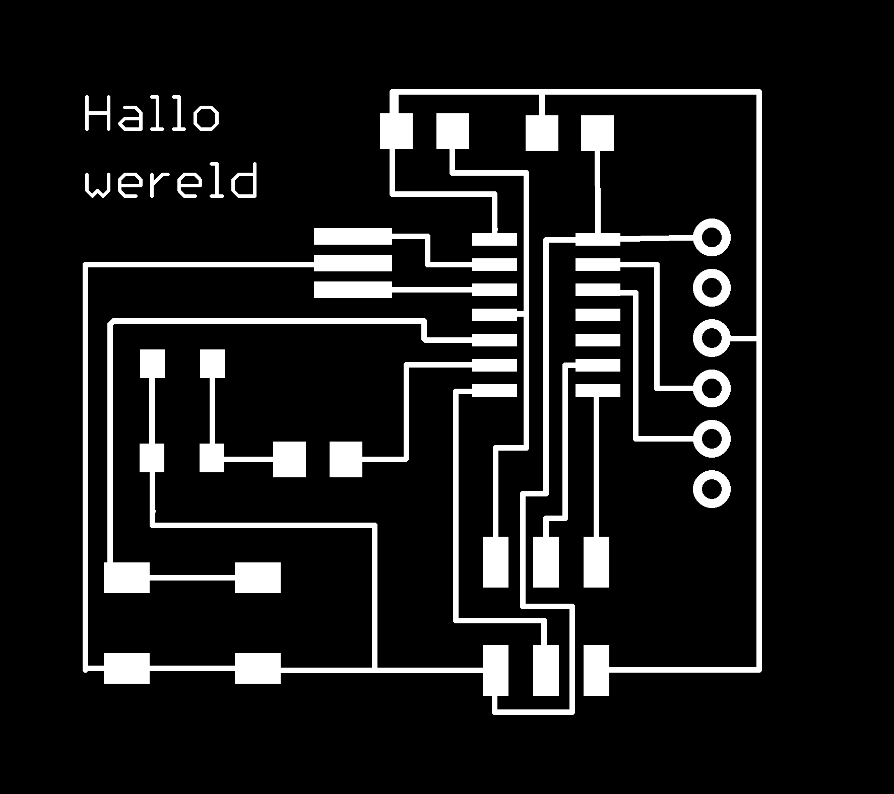 This is what the design of my hello-world board looked like This is what the design of my hello-world board looked like
1. Draw a schematic of the circuit
We decided to use Eagle, a programme that is quite different from most design programmes like illustrator and Rhino. The tutorials on youtube are very useful to get started.Eagle works with two modes: the schematic layout and the board layout. First the schematic has to be done. From a library you can add electronics parts, place them in the drawing area, and connect them to form a circuit.
For the hello world board, additional libraries with specific components are needed. They can be downloaded from the class site and the Sparkfun page. Download the .lib docs and open them in Eagle. Now it is possible to browse through the components by clicking the 'add' button.
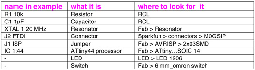
Figuring out which components were needed took most of the time of the assignment, since the names on the example were not corresponding with the names in the parts library, that contains hundreds of parts. Therefore I wrote down where I found them within the library:
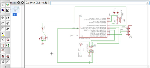
Putting the components together was not so hard, because the pins of the ATtiny have tags that give clues on which component needs to be connected. The green lines between the components can overlap, just like insulated wires can overlap without connecting. If they do connect a green dot must be drawn to indicate the junction. The result looked like this:
2. organize the components on the board
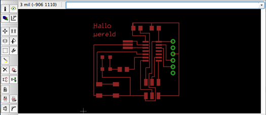
By pressing the 'board' button Eagle switches to its other mode, where the details on the board can be defined. Here the components need to be organized - the yellow lines indicate how they should be connected. It is a bit of a puzzle to find out how to connect the lines in a way that they do not cross or overlap.
3. create the milling paths and export to .png
When they are organized efficiently the routing paths can be drawn. I think that after some practice one could make the most beautiful patterns!
We did the routing lines in the top layer (red), and the outlines of the board in the white dimension layer. The size of the board can be drawn with the polygon tool. To fill the shape the ratsnest tool is used. The connections can be checked with the eye button. When clicking one piece on the board, all its connections are highlighted as well. To make sure the paths will be milled out correctly, these design rules can be followed. This is the drawing of the board:
When the design looks good and is checked it can be exported to a monochrome .png file on 1000 dpi.
4. mill the board
This was the same procedure as last week, but this time we had to solve some errors because some lines were a bit too close, so the milling bit would not fit in between. Picture will come.
5. solder the components
|
 Astrids Fab Academy Projects