Research
Electronics
Electronics studies the behavior of electrons and uses it to control, process, and transmit information by manipulating electric currents and semiconductor materials.
Useful Sources
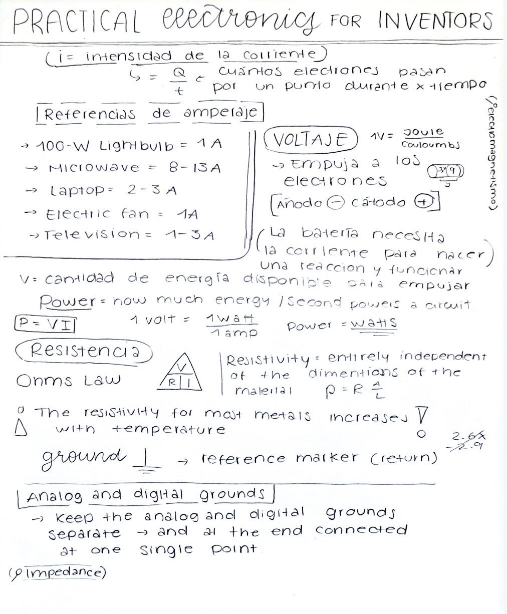
For this week first I tried to understand electronics and its basic concepts
To do this I took a youtoube basic electronics course and started reading the book "Practical electronics for inventors", Here are the sources:
🖱️ Click: Youtube course🖱️ Click: Book
I took a lot of notes, in the image you can see one of my summaries.
Electronics design softwares
There are different design softwares like: Altium and KiCad.
I used KiCad because it is free and I found a lot of tutorials.
PCB design
Since it is my first PCB i wanted it to be multifunctional and versatile. I got inspired by Adrian Torres's 🖱️ Click: Fab Xiao board. It's made up of several pin headers so I can connect other things later, and it also has an I2C section, which will be useful later in the inputs week.
Simulation
Why simulate?
Simulation is a way to test your circuit before building it in real life. It helps you understand how electricity flows, how components behave, and if your design will work correctly. By simulating the circuit, you can detect mistakes early, adjust values like resistors, and visualize voltage and current without risking damage to real components.
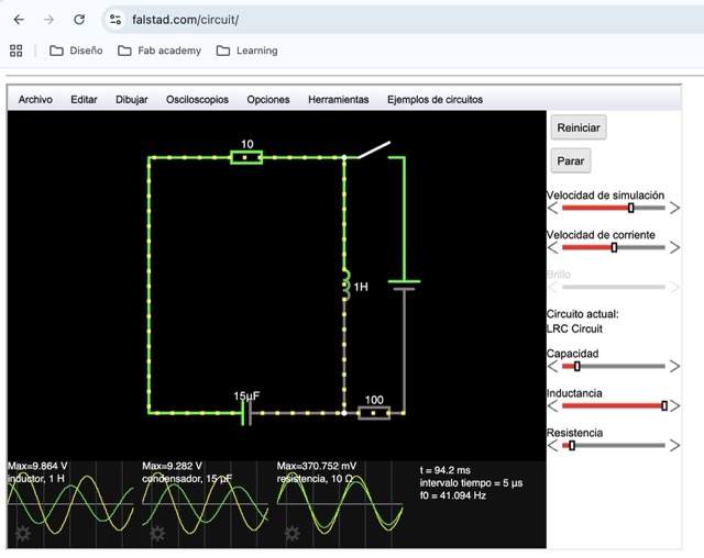
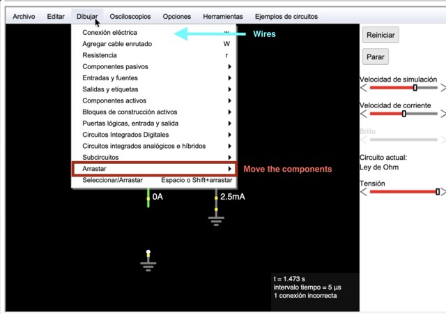
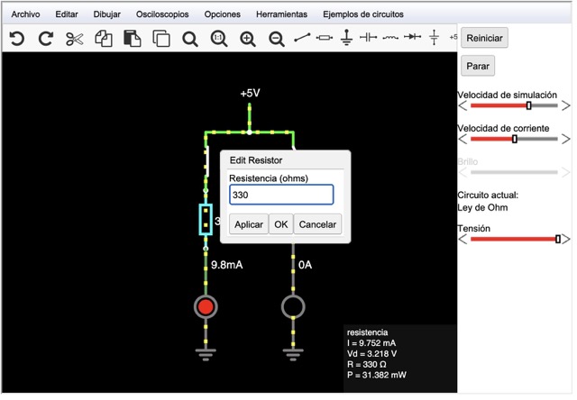
Electronic Simulation on Falstad
I used Falstad for my simulation because it is a great browser-based circuit simulator. I used it to visualize the actual current flow and get a better grasp of voltage and current. Slide through to see how I set it up.
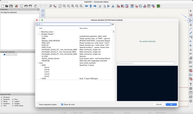
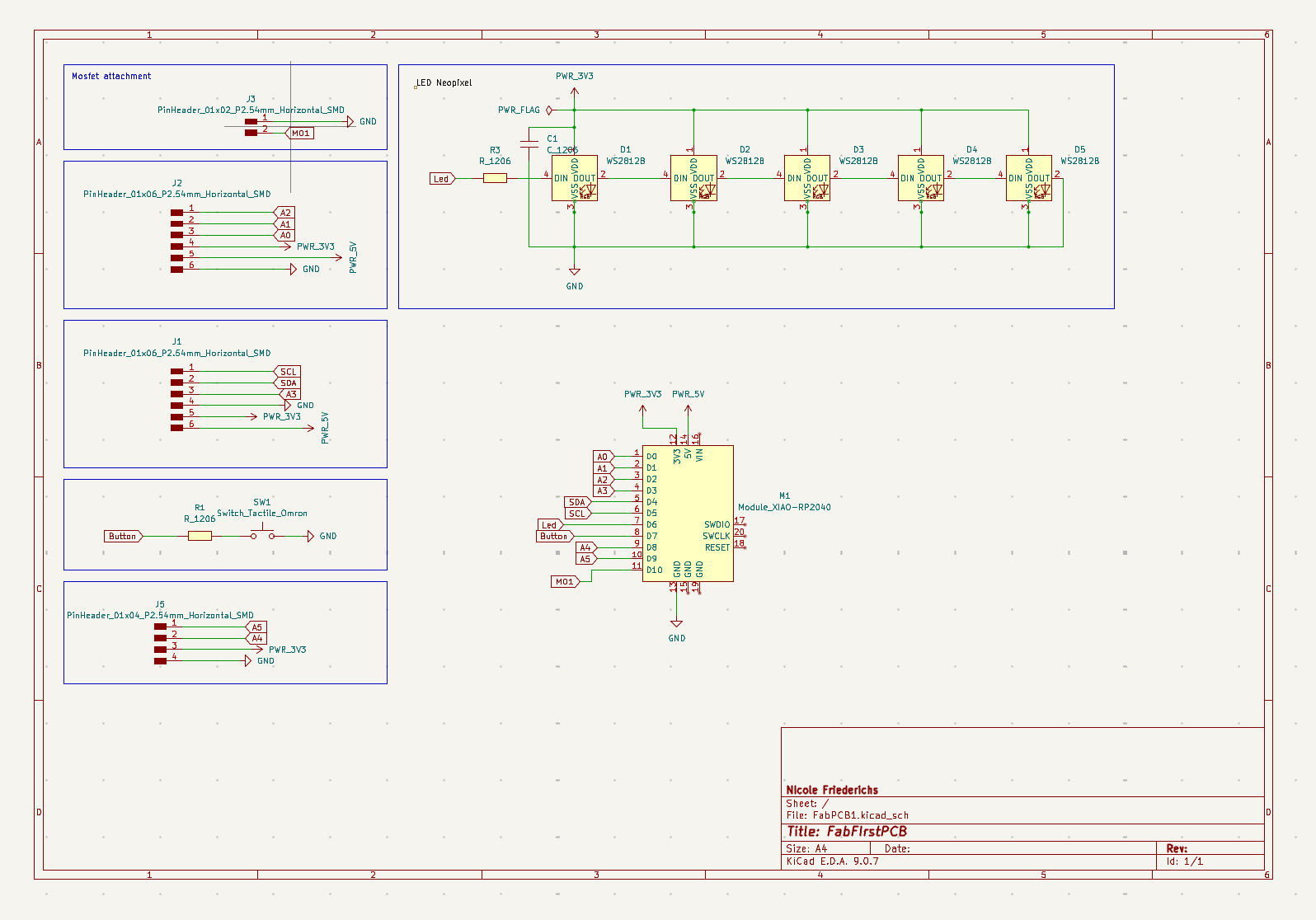
Schematic
Schematic
The schematic is a diagram that represents how all the electronic components are connected. It is like a map of the circuit. This step is important because it defines the logic of the system before creating the physical board.
STEPS:
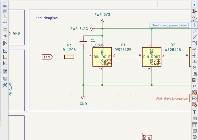
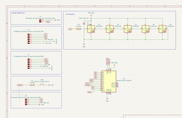
Final Result:
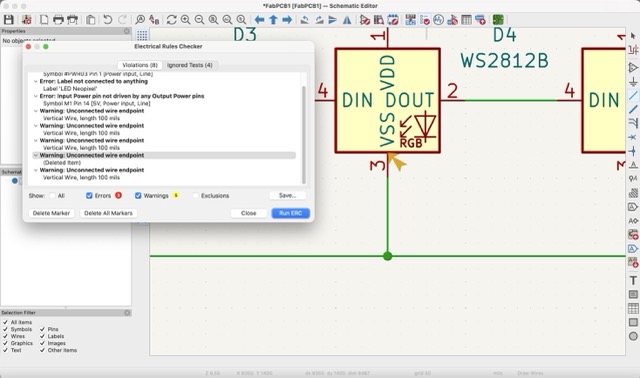
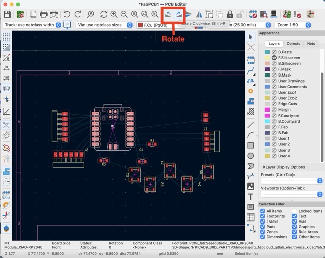
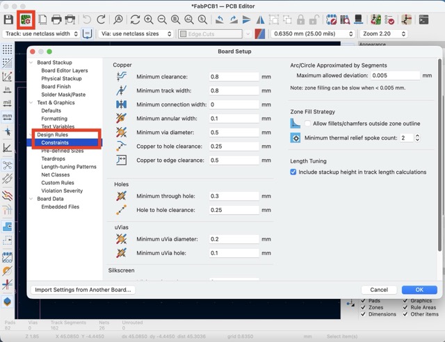
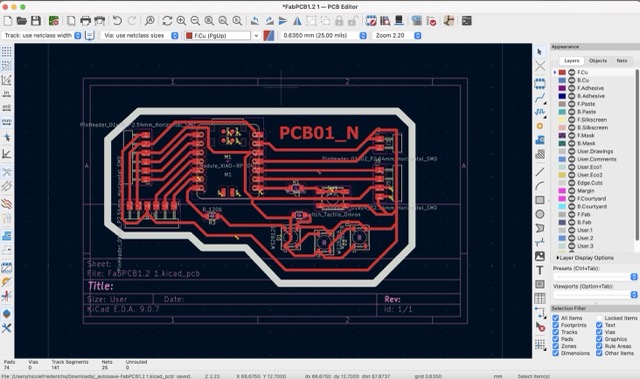
PCB Design
PCB design is the process of transforming the schematic into a physical board. In this step, components are placed and connected using copper traces. A good PCB design ensures that the circuit works correctly and can be manufactured easily.
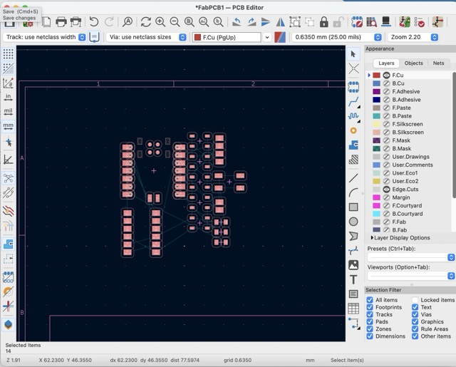
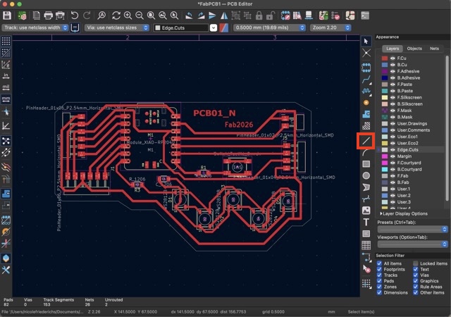
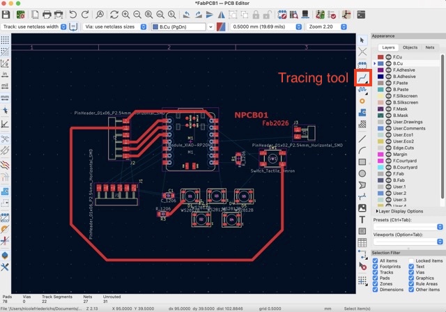
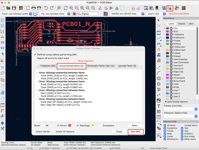
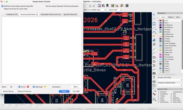
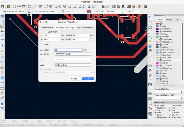
Final Result:
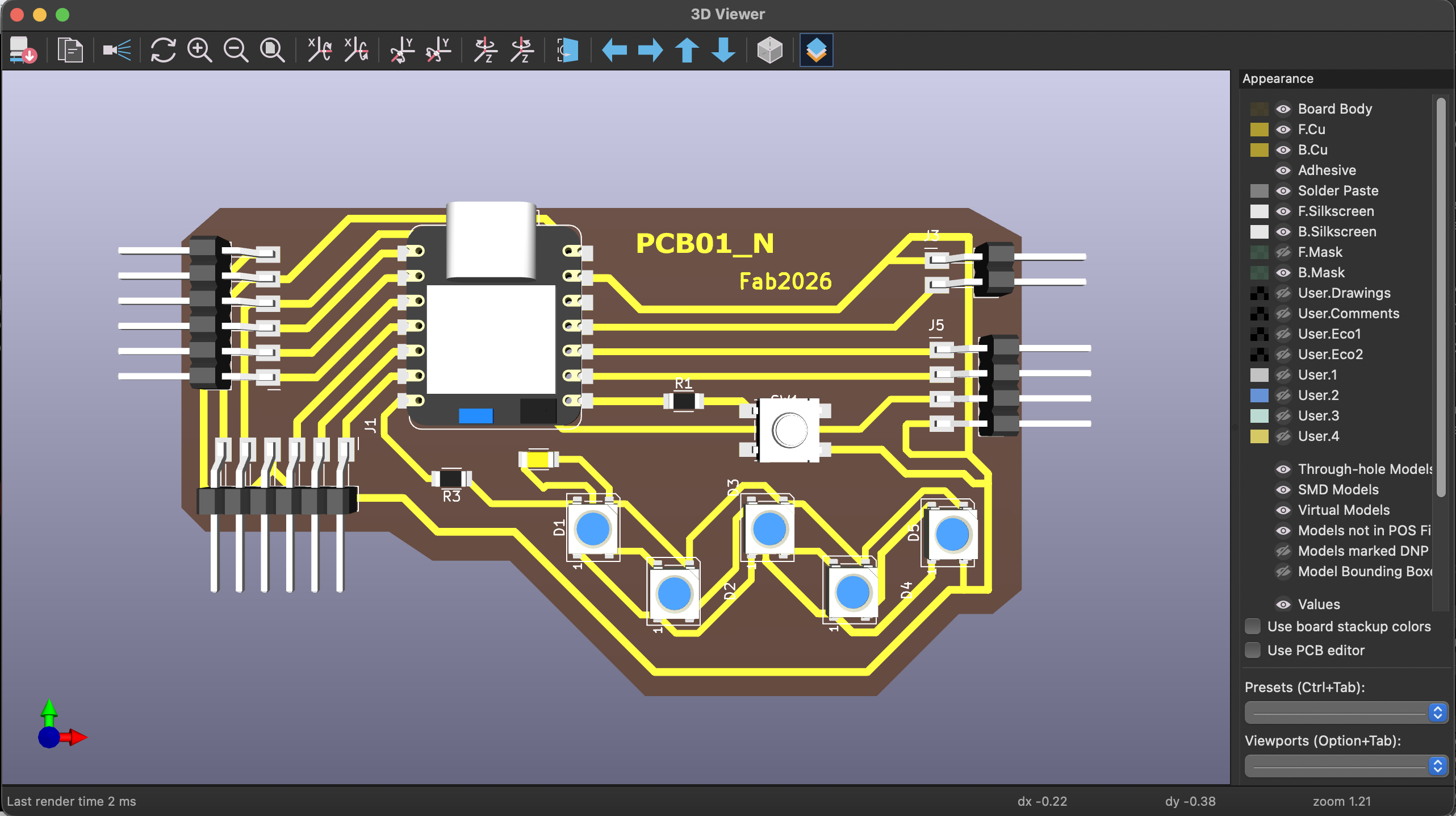
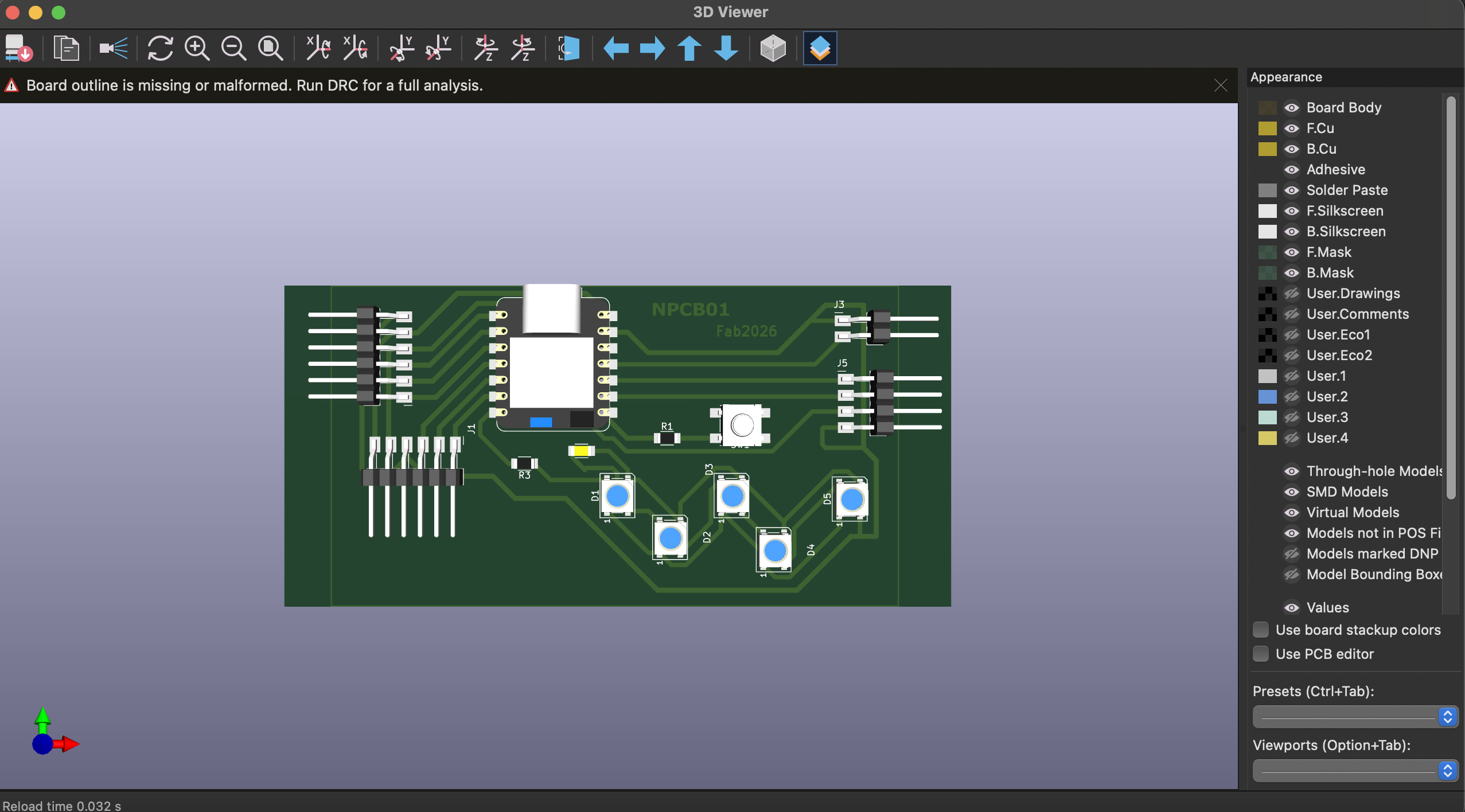
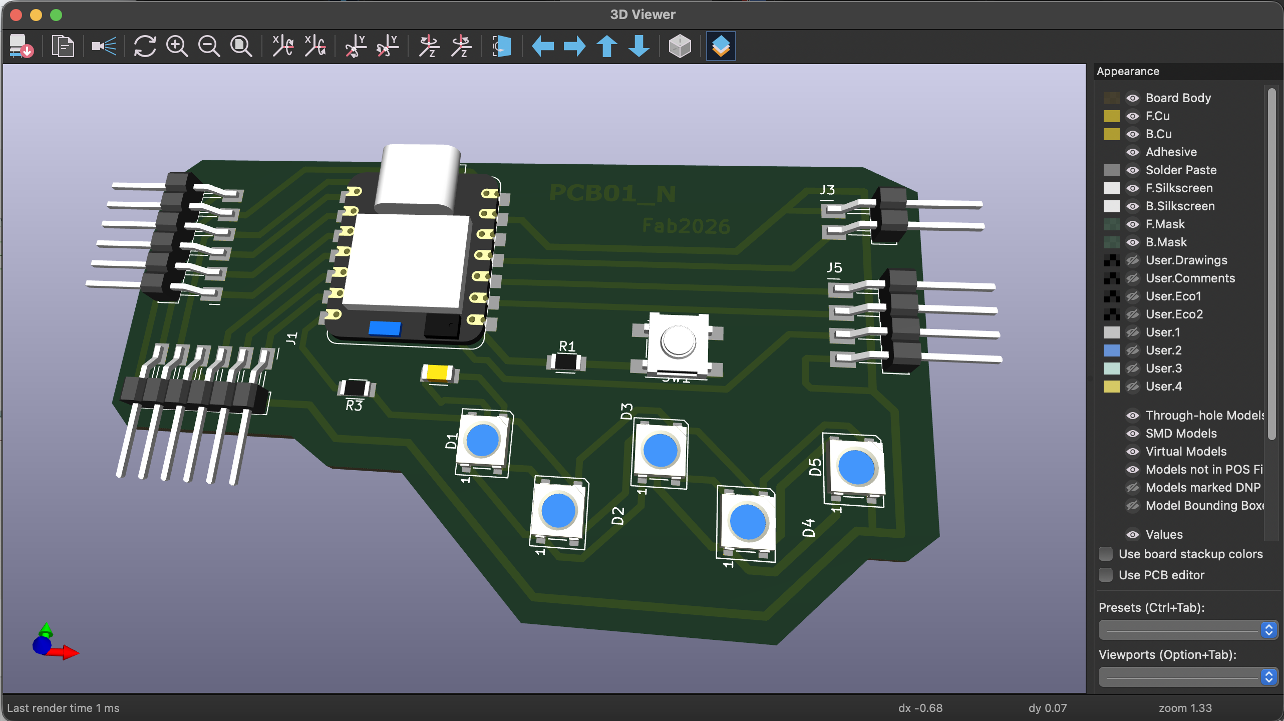
3D viewer
The 3D Viewer allows you to visualize your PCB as a real object. This helps you understand how the final board will look and check the placement of components. It is useful for detecting design issues and preparing for enclosure design.
Steps:
1. Open the 3D Viewer from the View menu or by pressing Alt + 3.
2. Explore the board by rotating and zooming to check how all components are placed. (I had to adjust the border to make sure that the pinheaders would stand out)
3. If you want to design a case, export the PCB as an STL or STEP file from the PCB editor.
Final Result: