Week 08
Electronics Production
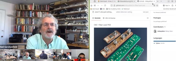
Class with Neil
During Week 08 – Electronic Production, the main objective was to design and fabricate our own Printed Circuit Board (PCB). This process involved transforming a digital electronic design into a physical board by using digital fabrication tools available in the Fab Lab.
The workflow included key stages such as circuit design, component selection, PCB layout, toolpath generation, and machining using a CNC milling machine. Through this process, we learned how to properly translate schematics into a manufacturable board, considering aspects such as trace width, component placement, and electrical connections.
This assignment allowed me to better understand the complete production cycle of electronic boards, from design to fabrication, strengthening both my technical skills and my knowledge in electronics manufacturing.
Have you answered these questions?
- I. Linked to the group assignment page. ✅
- II.Documented how you made the toolpath ✅
- III.Documented how you made (milled, stuffed, soldered) the board ✅
- IV. Documented that your board is functional✅
- V. Explained any problems and how you fixed them ✅
- VI.Uploaded your source code✅
- VII.Included a ‘hero shot’ of your board✅
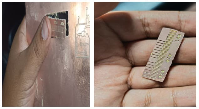
Hero Shot
This image shows the final result of my Electronics Production assignment, where I manufactured a board designed for sensor interaction and embedded programming. Through this assignment, I learned the importance of precision during the electronics production process, especially while soldering small components and verifying electrical connections. I also understood how proper PCB design and clean assembly improve both the functionality and reliability of the circuit. The final prototype demonstrates the integration between electronics production and embedded systems, resulting in a functional board capable of communicating with external sensors in real time.
Group Assignment:
°Characterize the design rules for your in-house PCB production process: document the settings for your machine.
° Document the workflow for sending a PCB to a boardhouse
° Document your work to the group work page and reflect on your individual page what you learned
Group Assignment
For the group assignment, we worked together to understand the PCB production process using the available machines in the Fab Lab. As a team, we explored how to prepare the design files, generate the toolpaths, and configure the CNC milling machine for both traces and cutting operations.
We tested different parameters such as cut depth, feed rate, and tool selection to ensure clean and precise milling of the PCB. This helped us identify the correct settings needed to avoid issues like incomplete traces or damaged boards.
Through this collaborative process, we gained a better understanding of how the PCB fabrication workflow works and how small adjustments in parameters can significantly affect the final result. This experience was important to ensure success in our individual PCB designs. ⚙️💡
1.Router Tools Used
For the PCB fabrication process, we used a Roland SRM-20 CNC milling machine, which provides high precision for electronic production in Fab Labs. During the machining process, different milling bits were selected depending on the task: 0.1 mm and 0.5 mm bits were used for fine traces to achieve detailed and accurate circuit paths, while a 2 mm bit was used for cutting and defining the board outline. The correct selection of these tools was essential to ensure clean results, avoid errors in the traces, and obtain a well-fabricated PCB. ⚙️💡
🔩 0.5 mm 30° V-Bit (o V-Carving Bit)
This milling tool is primarily used for CNC machines and is made of tungsten steel, which provides high durability and precision during machining. It features a 3.175 mm shank, a 0.5 mm cutter tip, and a 30° tip angle, making it suitable for detailed and fine cutting operations. This type of tool is commonly used for processing materials such as bakelite, acrylic, PVC, wood, MDF, and similar derivatives, allowing clean and accurate results in PCB and general fabrication tasks.
🔩 2 mm Carbide End Mill (Flat End Mill)
The 2 mm Carbide End Mill is a flat-end cutting tool widely used in CNC machining for precise cutting and material removal. It is made of tungsten carbide, which provides high hardness, durability, and resistance to wear, while the titanium coating helps reduce friction and improves tool lifespan.
This tool features a 3.175 mm shank diameter, a 2 mm cutting diameter, and a 12 mm cutting length, making it suitable for detailed cutting tasks. It is commonly used for PCB cutting, MDF, and plywood, especially for contouring and profiling operations. Due to its flat tip, it allows clean edges and accurate cuts, making it ideal for defining the final shape of machined parts. 🔩
🚪 Bakelite 1.6 mm PCB Material
The 1.6 mm Bakelite board is a commonly used substrate for PCB fabrication, especially in CNC milling processes. It is made from phenolic resin and paper layers, providing a rigid and stable structure suitable for electronic circuits. This material is widely used due to its good electrical insulation properties, low cost, and ease of machining.
With a thickness of 1.6 mm, it offers an ideal balance between mechanical strength and workability, making it suitable for both traces milling and board cutting. Bakelite is compatible with CNC tools such as V-bits and end mills, allowing precise fabrication of circuit paths and clean board outlines. Additionally, it is a reliable option for prototyping electronic boards in Fab Lab environments. ⚙️💡
📟Group Challenges
During the group work, one of the main challenges was coordinating the use of the CNC machine and organizing the workflow among team members. Since several people needed to use the equipment, we had to carefully plan the machining times and preparation steps to avoid delays.
Another challenge was ensuring that everyone correctly understood the CNC preparation process, including setting the X, Y, and Z axes, fixing the material properly on the machine bed, and verifying the toolpaths before starting the cutting process. Small mistakes in these steps could affect the machining results.
Through collaboration and discussion, we were able to solve these issues by helping each other review the machine setup, checking the files before cutting, and sharing our observations during the fabrication process. This teamwork helped us achieve more accurate and safer results when using the CNC router. ⚙️🪵
🔍 Refletions
During this assignment, I gained a deeper understanding of the complete PCB fabrication process, from design to physical production. Working with the CNC milling machine allowed me to appreciate the importance of selecting the correct tools, materials, and parameters to achieve precise and reliable results.
One of the key learnings was how small adjustments in settings, such as cut depth and tool selection, can significantly affect the quality of the PCB traces. I also reinforced the importance of careful preparation, including verifying the design files and ensuring proper machine setup before starting the milling process
Overall, this experience helped me strengthen my skills in digital fabrication and electronics production, while also highlighting the importance of attention to detail and continuous testing to achieve successful results. ⚙️💡
Individual Assignment
° Make and test a microcontroller development board that you designed
1. Introduction
During this week, I focused on developing my own PCB (Printed Circuit Board) as part of the Electronic Production assignment. I worked on the complete process, starting from the circuit design to the fabrication using a CNC milling machine.
Through this experience, I was able to understand how to transform my electronic design into a physical board, taking into account important aspects such as tool selection, material properties, and machining parameters. This assignment helped me strengthen my skills in electronics and digital fabrication, while gaining hands-on experience in producing functional PCBs. ⚙️💡
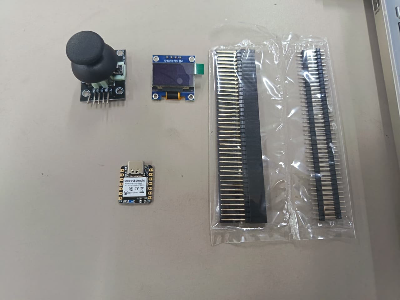
PCB Components List
| Item | Component | Amount |
|---|---|---|
| 1 | SEEED STUDIO XIAO RP2040 | 1 |
| 2 | Header 01x05 P2.54 mm Horizontal SMD | 4 |
| 3 | Resistor 1KΩ 1% 1206 | 3 |
| 4 | Green LED 1206 SMD | 2 |
| 5 | OLED Display (128x64 I2C) | 1 |
| 6 | Joystick Module | 1 |
📟PCB Components
This PCB integrates the Seeed Studio XIAO ESP32-S3 as the main microcontroller responsible for processing data, controlling peripherals, and managing communication between all components in the system. The board also includes an OLED display module, used as the visual output device to display information, sensor values, and interface elements in real time. Additionally, a joystick module is connected as the main input device, allowing directional control and user interaction through analog movement signals. 🎮📟⚙️
These components work together to create an interactive embedded system where the joystick sends input data to the ESP32-S3, and the microcontroller processes the information to generate visual feedback on the OLED display. This configuration demonstrates the integration of both input and output devices within a compact custom PCB design.
📍 2. Ubication
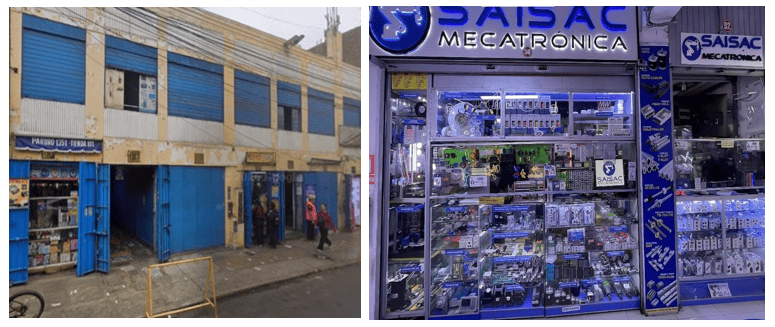
The electronic components used in this project were sourced from Saisac Mecatrónica, a specialized electronics supplier located in the city of Lima. This store offers a wide range of components suitable for PCB design and prototyping. For reference, the exact location of the store can be accessed through Google Maps at: Jr. Paruro 1349, Lima 15003.
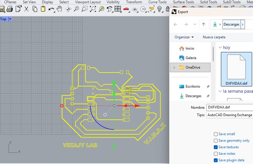
📈3. Importing DXF Files into Rhino:
After completing the PCB design in KiCad, I exported the board layout in a compatible format (such as SVG or DXF) to be used in Rhinoceros. This step allowed me to work with the PCB geometry in a more flexible environment for visualization and additional adjustments.
Once imported into Rhinoceros, I verified the scale, alignment, and dimensions of the traces and board outline to ensure accuracy. This process helped me prepare the design for further processing, such as organizing layers, refining details, or generating toolpaths for CNC machining.
Using Rhinoceros as an intermediate tool allowed me to have better control over the geometry and ensured that the final design was clean and ready for fabrication. 📐⚙️
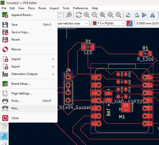
⚙️4. Import of KiCad to Rhinoceros
After completing the PCB design in KiCad, I proceeded to export the board layout using the Plot tool. In the window that appears after clicking Plot, I verified that the size was correctly updated, selected the units in millimeters, and then clicked Plot to generate the file. The design was automatically saved in the specified output directory.
This exported file was then imported into Rhinoceros, where I checked the scale and geometry to ensure everything was accurate and ready for further processing before fabrication. 📐⚙️
.jpeg)
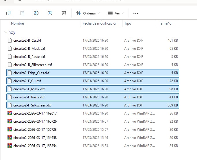
⚙️4.1 Selection of the files to Import
Once in the directory, I open the DXF files marked in a green box, using the Rhinoceros program.
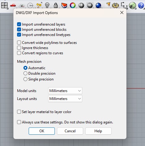
⚙️5. Verifying the units of the model and layaout
Once in the Rhinoceros program, I verify that both the model units and the layout units are also set to millimeters and click OK.
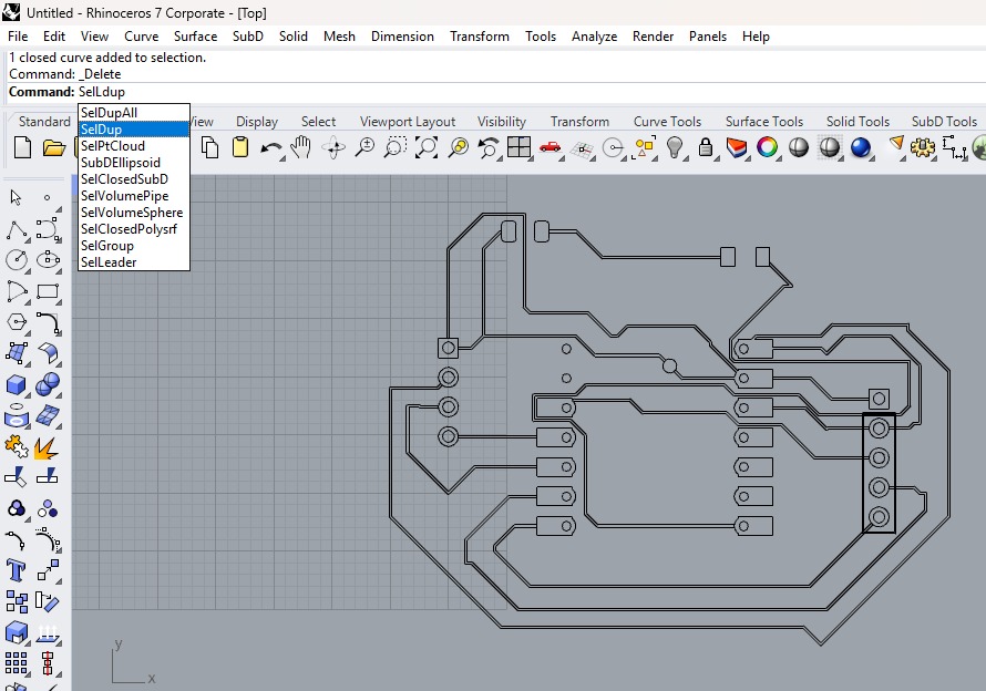
⚙️5.1 Cleaning and Preparing PCB Geometry in Rhinoceros
In this step, the PCB design previously imported from KiCad is being refined Rhinoceros 7. The image shows the use of the SelDup (Select Duplicates) command, which is essential for identifying and removing duplicate curves that may have been generated during the export or import process.
Cleaning duplicate lines is a crucial step because overlapping geometries can cause issues when generating toolpaths for CNC milling, leading to incorrect cuts or tool errors. After selecting and deleting duplicates, the geometry becomes cleaner and more reliable for further processing.
⚙️5.2 Exporting Files for CNC Routing (Aspire)
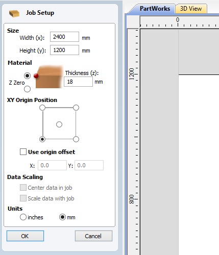
After cleaning and verifying the PCB geometry in Rhinoceros, I proceeded to export the design in a format compatible with Aspire or ShopBot software to begin the routing process. For this, I exported the file as a DXF, ensuring that all curves were properly joined, scaled in millimeters, and organized correctly.
Once imported into Aspire, I configured the workspace according to the material dimensions and thickness. Then, I assigned the corresponding toolpaths for each operation, such as trace milling and board cutting, selecting the appropriate tools and parameters (cut depth, feed rate, and spindle speed).
⚙️5.3 Selecttion of the Files
Once in the Rhinoceros program, I verify that both the model units and the layout units are also set to millimeters and click OK.
Through this program, I prepared the machine to start the fabrication process. Once the file was loaded, the CNC machine followed the programmed toolpaths to cut the parts from the bakelite accurately, allowing the components of the shelf to be produced for the assembly stage. ⚙️🪵
⚙️5.4 Selecttion of the Files
After generating the toolpaths, I saved the G-code file and transferred it to the CNC machine. The file was then loaded into the ShopBot3 Router control software, which is used to operate the CNC router.
Through this program, I prepared the machine to start the fabrication process. Once the file was loaded, the CNC machine followed the programmed toolpaths to cut the parts from the bakelite accurately, allowing the components of the shelf to be produced for the assembly stage. ⚙️🪵
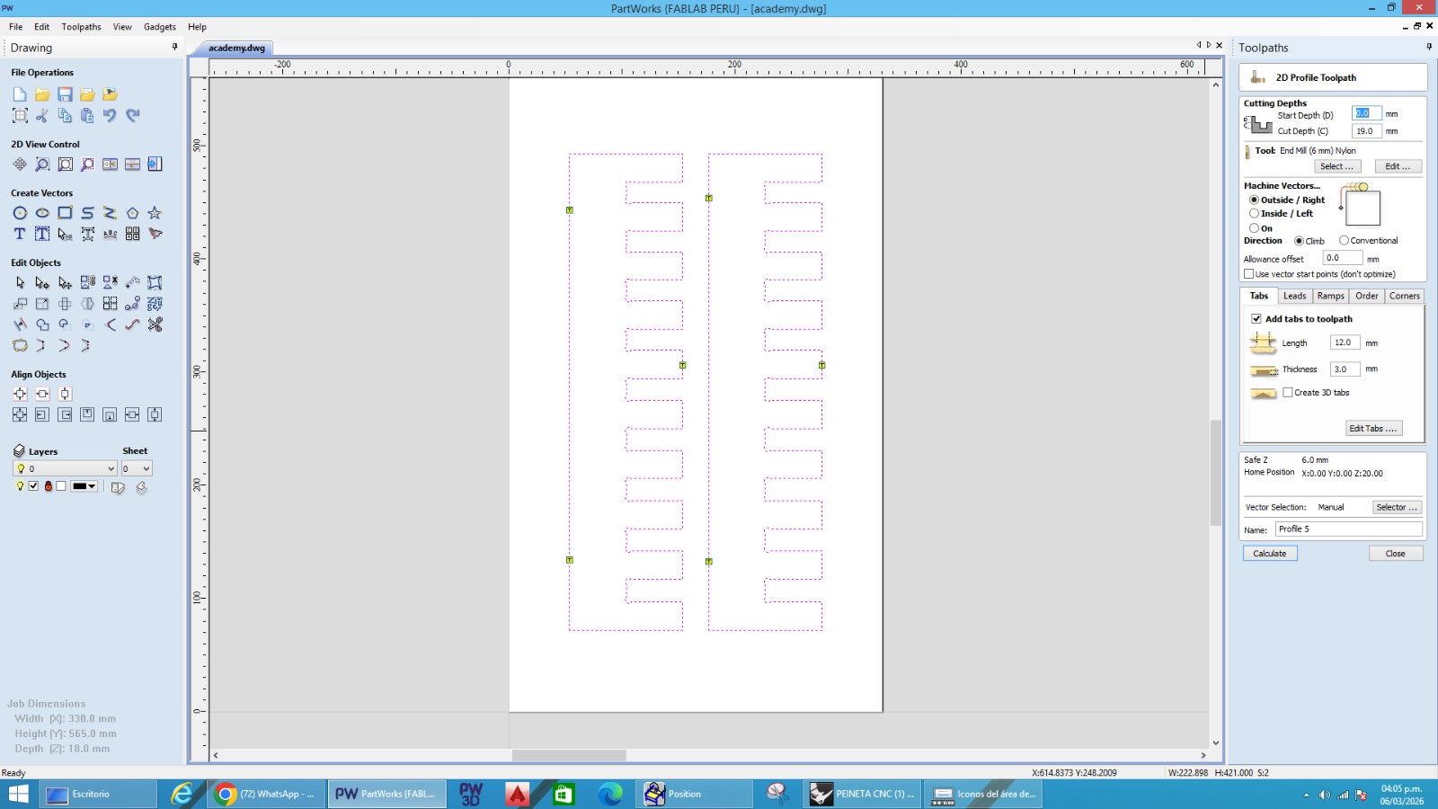
⚙️5.5 Toolpath Generation and Manufacturing Setup
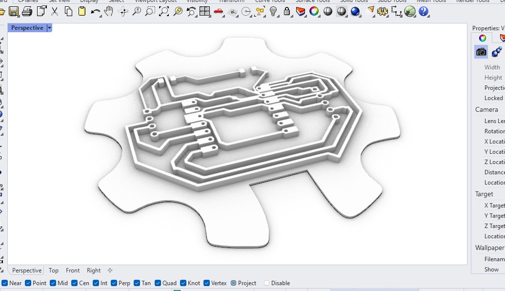
This image shows the toolpath generation process used during the PCB manufacturing stage inside the CAM software. The PCB traces and board outline were imported and configured using a 2D Profiling Toolpath strategy, where the purple lines represent the milling paths that the CNC machine would follow during fabrication. For this process, I selected a 1 mm universal milling bit to machine the PCB contours and copper isolation areas with precision. The machining configuration included an initial depth of 0.0 mm and a final depth of 1.8 mm, allowing the tool to properly cut through the PCB material while maintaining accurate trace definition.
Additionally, the machining direction was configured as Outside / Right using a climb cutting strategy, helping improve cutting quality and edge finish during the milling process. A safe Z height of 5 mm was also configured to avoid collisions during rapid movements between toolpaths. This toolpath preview was essential to verify the manufacturing workflow before fabrication, since it allowed me to confirm the trace isolation, cutting boundaries, milling direction, and overall PCB machining strategy prior to generating the final machine file for CNC production.
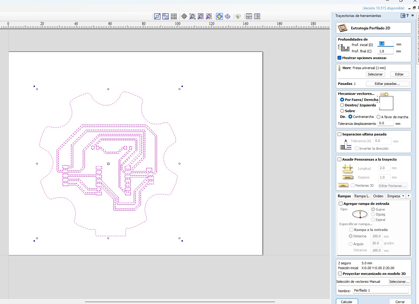
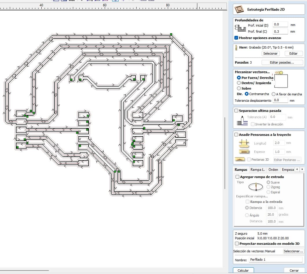
⚙️5.6 PCB Trace Milling Configuration
This image shows the detailed toolpath configuration used for machining the PCB traces during the electronic production process. In this stage, the CAM software generated multiple isolation paths around the copper traces to ensure proper electrical separation between connections on the board. The arrows visible along the paths indicate the milling direction that the CNC machine would follow while engraving the PCB surface. For this operation, a 20° engraving milling bit (0.5–6 mm) was selected to achieve finer and more precise trace isolation suitable for PCB fabrication.
The machining setup was configured with an initial depth of 0.0 mm and a final cutting depth of 0.3 mm, using 3 machining passes to gradually remove material while protecting the PCB surface and improving milling accuracy. The machining strategy was configured as Outside / Right with a climb milling direction, while maintaining a safe Z height of 5 mm during rapid movements. This preview allowed verification of the trace spacing, isolation quality, cutting directions, and overall manufacturing strategy before generating the final machining file for CNC PCB production.
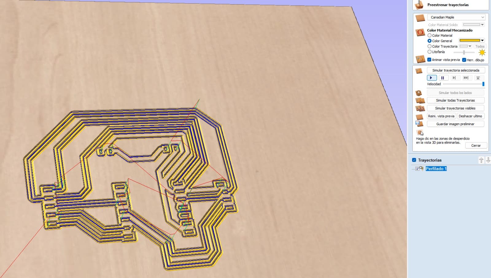
⚙️5.7 3D Toolpath Simulation
This image shows the 3D simulation of the PCB machining process before fabrication. The CAM software generated a visual preview of the engraving toolpaths, allowing verification of the copper isolation paths, trace spacing, and overall PCB geometry. The blue and yellow lines represent the milling trajectories that the CNC machine would follow during the manufacturing process.
The simulation was important to validate the PCB before machining because it helped confirm that all traces were correctly isolated and that the cutting paths were properly generated. This preview also reduced possible fabrication errors by allowing me to inspect the machining result virtually before exporting the final CNC production file.
⚙️5.8 Debugging and Testing Evidence
During the debugging and testing stage, the PCB milling process on the Roland SRM-20 presented an error caused by insufficient double-sided tape placed under the bakelite board. Because the material was not firmly fixed to the machine bed, the board moved slightly while the milling tool was engraving the traces. As a result, some PCB paths became misaligned and the final engraving quality was affected. ⚠️🛠️
This test was important to identify the importance of properly securing the material before starting the machining process. After analyzing the issue, additional double-sided tape was added to improve stability and ensure that the PCB remained completely fixed during operation. This debugging process helped improve the manufacturing workflow and avoid positioning errors in future milling attempts.
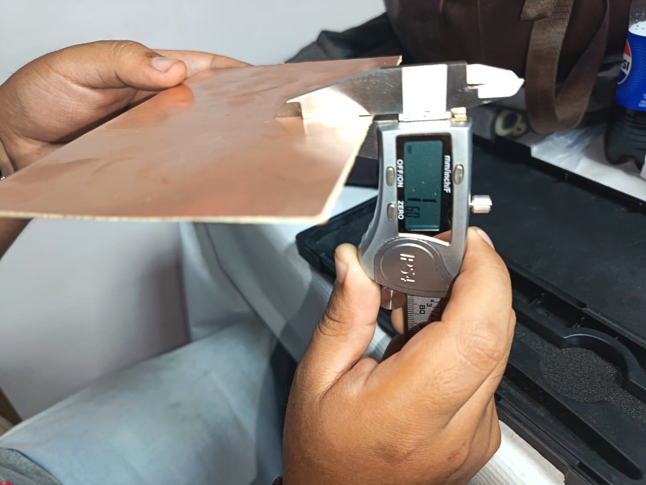
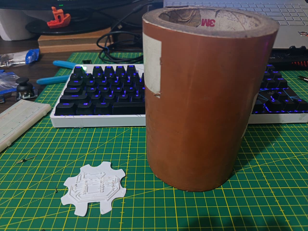
⚙️6. Material Selection:
For this project, I selected 1.6 mm bakelite as the main material for the fabrication of the shelf. This material was chosen because it provides good strength, durability, and stability
The thickness of 16 mm is a material that works well with CNC machining ROLAND, allowing clean and precise cuts during the milling process. 🪵⚙️
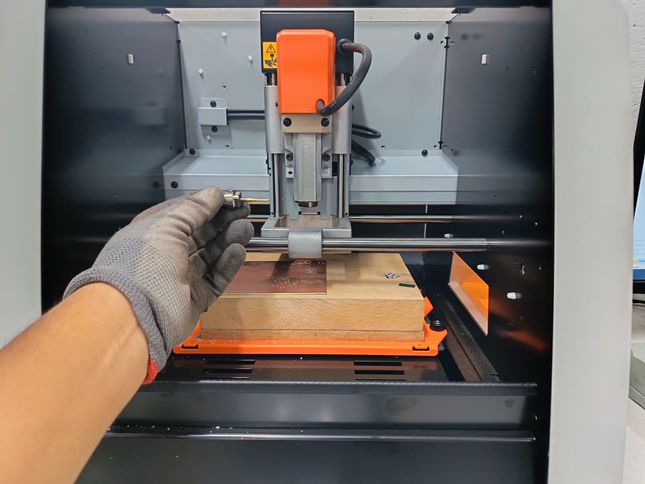
⚙️🪵7.Fixing the Material on the CNC Router ROland:
Before starting the milling process, I securely fixed the Bakelite board (1.6 mm) onto the working bed of the Roland CNC Router. To ensure stability, I used double-sided tape and made sure the surface was clean and flat to avoid any movement during machining.
Proper fixation is essential to prevent vibrations or displacement while the tool is operating, which could affect the precision of the PCB traces. I also verified that the material was well aligned with the machine axes and that the working area was correctly defined.⚙️📌
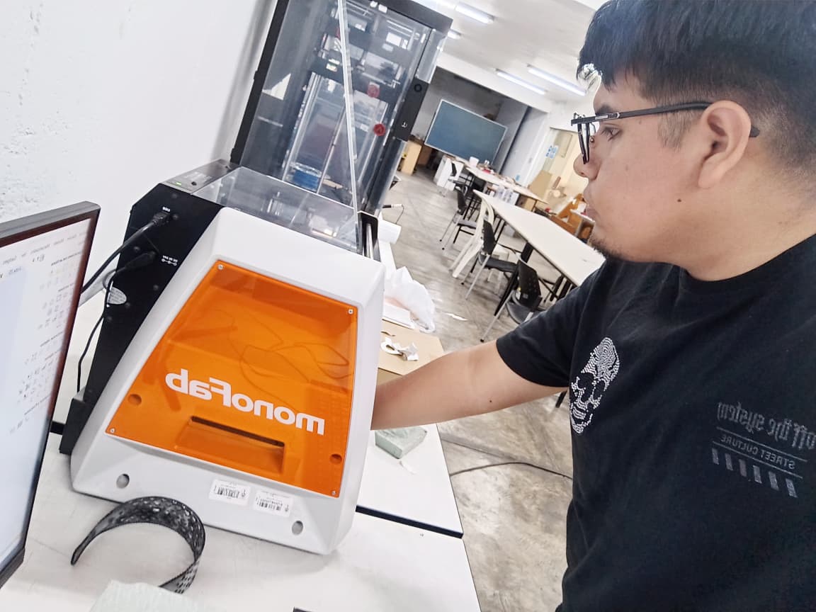
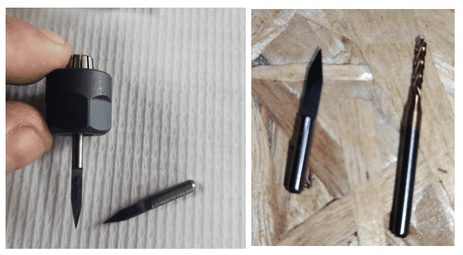
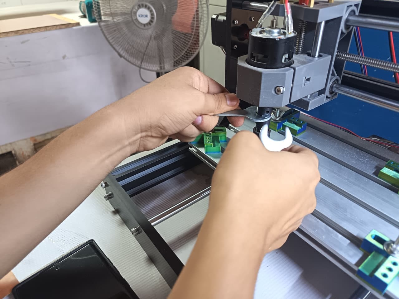
⚙️🪵7.1 Tool Setup and Bit Installation on Roland CNC
In this step, I prepared the Roland CNC Router by installing the appropriate milling bit for PCB fabrication. As shown in the image, I carefully placed the tool into the spindle while using protective gloves to ensure safety and avoid contamination or injury.
Proper tool installation is critical to achieve precise milling results. I made sure the bit was securely tightened and correctly aligned to prevent vibrations or tool displacement during operation. Additionally, selecting the correct tool diameter is essential depending on the level of detail required for the PCB traces.⚙️🛠️
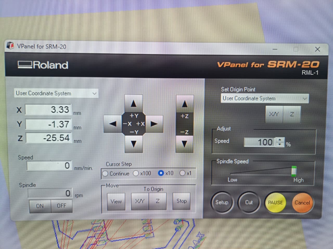
⚙️7.2 CNC Control with VPanel Software
To execute the milling process, I used the VPanel software from Roland, which allowed me to control the CNC machine and send the toolpaths. In this software, I uploaded the G-code files previously generated and configured the necessary parameters before starting the operation.
Through VPanel, I was able to manage key functions such as setting the origin point, controlling the spindle, and monitoring the cutting process in real time. Once everything was properly set, I initiated the milling process, allowing the machine to follow the defined toolpaths and fabricate the PCB accurately. ⚙️💻🛠️
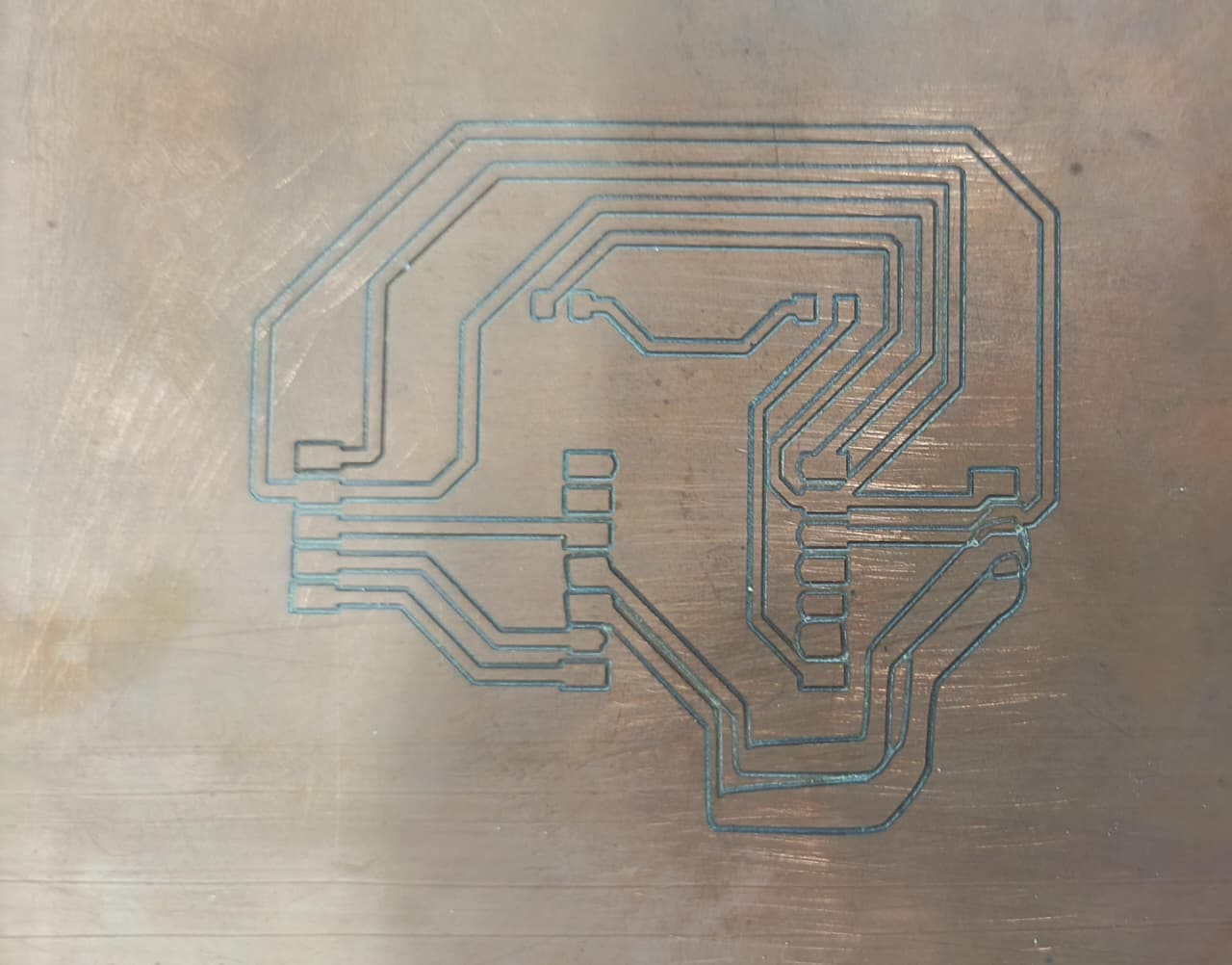
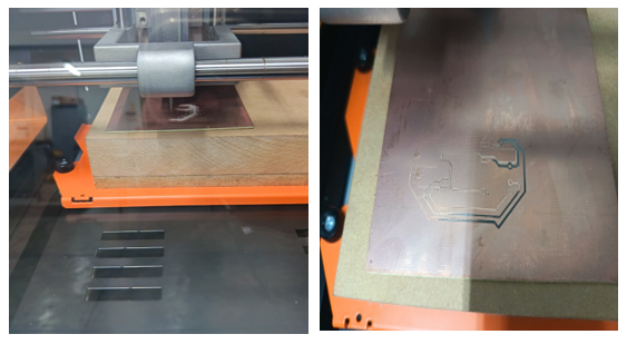
⚙️8. Cutting the Pieces:
Once everything was configured in VPanel, I started the cutting process on the Roland CNC Router. The machine followed the generated toolpaths to mill the PCB, beginning with the traces using a fine tool and then proceeding with the outline cut.
During this stage, I carefully monitored the process to ensure the cuts were clean and precise, verifying that the depth and alignment were correct. The material remained stable throughout the operation, allowing the milling bit to accurately remove the copper layer and define the circuit paths.This step was essential to transform the digital design into a physical PCB, ensuring proper electrical connections and a clean final result. ⚙️🔩
⚙️8.1 Debugging and Testing Evidence
During the debugging and testing stage, the PCB milling process on the Roland SRM-20 presented an error caused by insufficient double-sided tape placed under the bakelite board. Because the material was not firmly fixed to the machine bed, the board moved slightly while the milling tool was engraving the traces. As a result, some PCB paths became misaligned and the final engraving quality was affected. ⚠️🛠️
This test was important to identify the importance of properly securing the material before starting the machining process. After analyzing the issue, additional double-sided tape was added to improve stability and ensure that the PCB remained completely fixed during operation. This debugging process helped improve the manufacturing workflow and avoid positioning errors in future milling attempts.
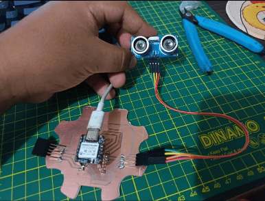
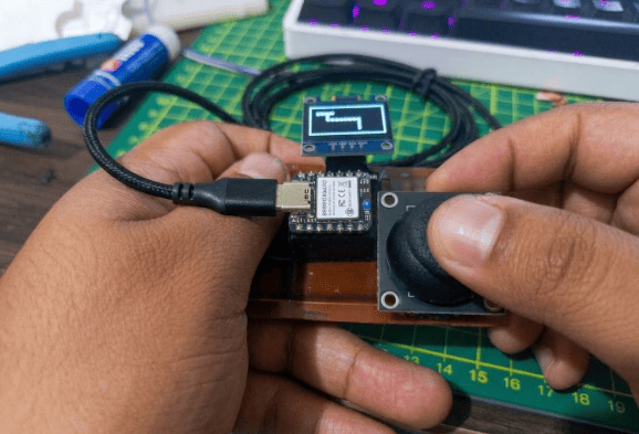
⚙️9. Assembly Debugging / Testing Evidence
This image shows the testing and debugging stage of the custom PCB integrating the XIAO ESP32-S3, an OLED display, and a joystick module. During this process, the board was powered through USB while the joystick inputs were tested in real time to verify that the microcontroller correctly detected movement in different directions. At the same time, the OLED display was used to visualize the system response and confirm that the communication between the components was functioning properly. 🎮📟⚙️
This testing stage was important to validate the electrical connections, input signal reading, and display output of the PCB. By interacting directly with the joystick and observing the response on the OLED screen, it was possible to confirm that the embedded system was operating correctly and that the PCB design successfully integrated both input and output devices into a functional prototype.
⚙️10. Experimenting with news types of production:
Once I had the design exported in the RhinoCeros program, I started analyzing it and realized that, because it had lines and thicknesses, I could extrude it. While I was organizing FABLAB UNI, I found conductive tape.
⚙️11. Materials in this process:
| Item | Component | Amount |
|---|---|---|
| 1 | Conductive tape | 1 |
| 2 | 3D Printer | 1 |
| 3 | Cutter | 1 |
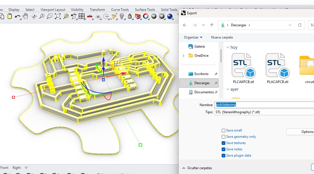
⚙️12. Export to a .STL document:
Once I have used the extrude tool in the design and have a 3D model, I export it in .stl format, and this will allow me to upload it to our preferred slicer.
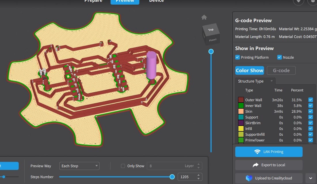
⚙️12.1 G-code Visualization and Toolpath Simulation:
In this step, I visualized the generated G-code using a preview interface, which allowed me to simulate the toolpaths before executing the fabrication process. The image shows a layer-by-layer representation of the PCB design, where different colors indicate specific movements such as outer walls, inner paths, and surface areas.
This simulation is important to verify that all traces, contours, and cuts are correctly defined, ensuring there are no missing paths or potential errors. It also provides an estimation of machining time and material usage, helping to optimize the process before actual production.
⚙️12.2 3D Printing Process:
In this stage, I carried out the 3D printing process to complement the PCB development. First, I prepared the model in a slicing software, where I configured key parameters such as layer height, infill, and printing speed. Then, I generated the G-code and reviewed the preview to ensure the geometry and paths were correct.
Once verified, I sent the file to the 3D printer and started the printing process. During fabrication, I monitored the first layers to ensure proper bed adhesion and overall stability. The printer then followed the defined paths layer by layer until completing the piece.
.png)
⚙️13.Applying Conductive Copper Tape
In this step, I used conductive copper tape and carefully applied it onto the surface of the 3D printed piece. First, I peeled off the protective layer of the tape and then aligned it with the printed PCB design to ensure proper coverage of the circuit paths.
I made sure the tape adhered smoothly to the surface, avoiding wrinkles or air bubbles that could affect conductivity. After placing it, I pressed it firmly so it could accurately follow the geometry of the printed traces.
.png)
⚙️14.Trimming and Defining the Circuit Paths
In this step, I carefully trimmed the excess copper tape to define the circuit traces on the 3D printed surface. Using a precision cutter, I removed the unnecessary material, following the design to isolate each path correctly.
This process required attention to detail to avoid damaging the conductive lines or breaking connections. After cutting, I verified that all the traces were cleanly defined and properly separated, ensuring correct electrical functionality.As a result, I obtained well-defined conductive paths, ready for the placement and assembly of the electronic components. ⚙️✂️
.png)
⚙️15.Final Assembly and Functional Prototype
In this final stage, I placed and connected the electronic components over the prepared conductive paths, creating a functional prototype of my PCB. This setup represents an initial version of my final project, allowing me to validate the design before manufacturing a more refined board.
In this case, I integrated an OLED display, which will serve as the main interface in the future, and a servo motor, which will act as the actuator for the pill dispenser mechanism. By assembling these components, I was able to test their interaction and verify that the circuit works as intended.This prototype approach helps me evaluate the system behavior, detect possible improvements, and move forward with a more optimized and reliable final design. ⚙️🔬
.png)
📟Difficulties (Individual)
During the fabrication process, I encountered an issue when trying to send the cutting job to the Roland CNC Router. There was a misconfiguration in the machine drivers, which prevented proper communication between the computer and the CNC..
This problem delayed the start of the milling process, as I had to review and correct the driver settings to ensure the machine was correctly recognized and could receive the G-code files. After troubleshooting and reconfiguring the drivers, I was able to restore the connection and continue with the fabrication process normally..
Files
Here are the project files available for download:
- DXF: Download .dxf
- FILE SPHIRE: Download .crv3d
- Gcode Generated: Download .rol