
Week 08
Week 08: Electronics Production
I simplified and produced a PCB, learned how in-house milling rules affect board design, and compared that path with board-house production for future project boards.
FINALLY, CREATING OUR OWN PCBs. This was the week we get started with it, but it was much harder than I thought and tackled a bunch of unexpected problems, but I figured it out at the end of the day :)
For this one, I was fully at my FabLab, and locked in on understanding the tools we have at the lab across the whole process of milling the board and soldering components on it.
Jump to this week’s checklist
Group Assignment: In-house PCB Production Design Rules and Sending PCBs to a Boardhouse
The group assignment this week had two parts. First, figure out the design rules of our in-house PCB mill. Second, walk a real design through the process of sending it to a board house. The full group write-up is linked here.
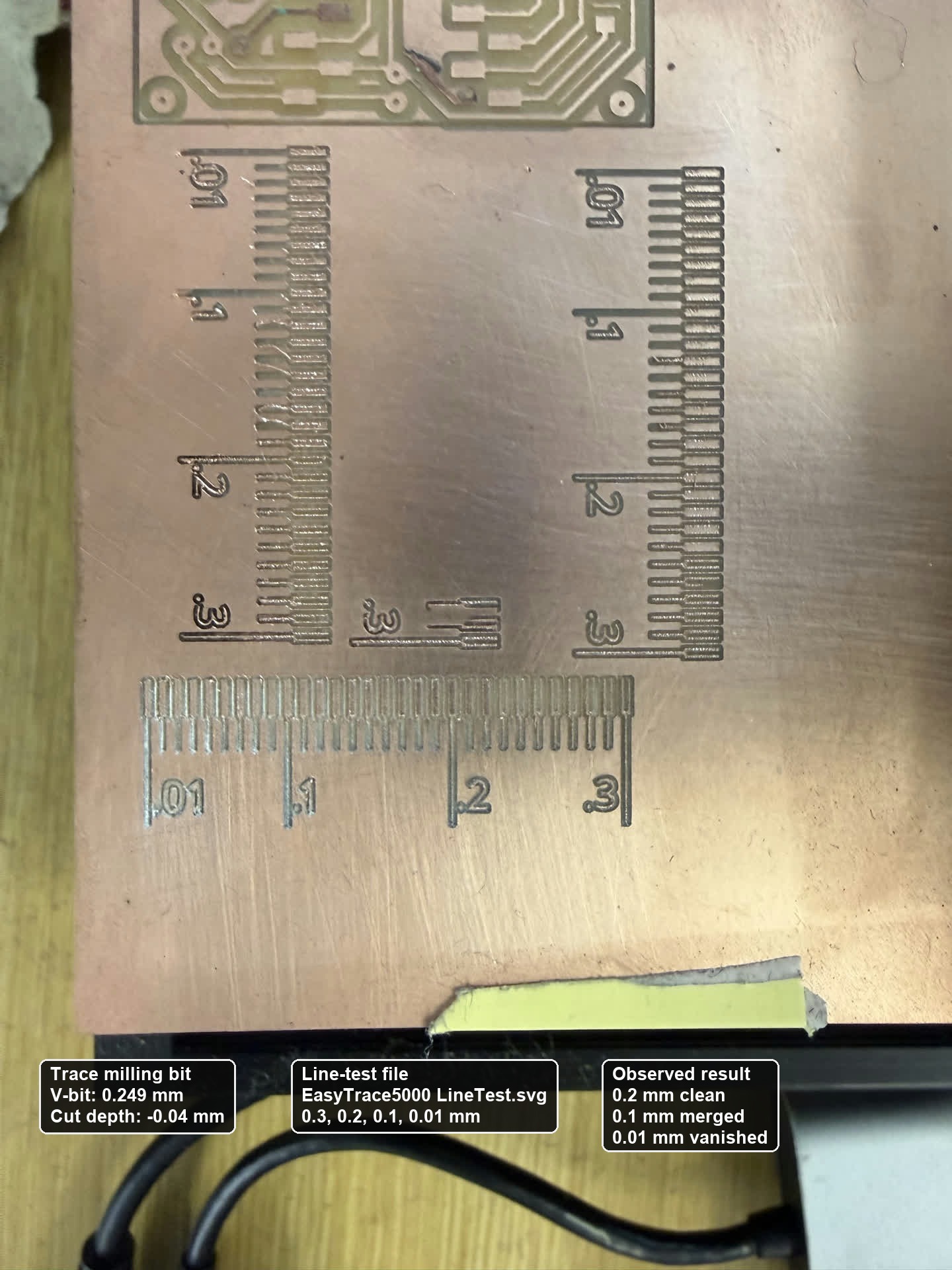
Design rules are the physical limits of our specific machine, and the only way to know them is to mill a test pattern and look at what survived.
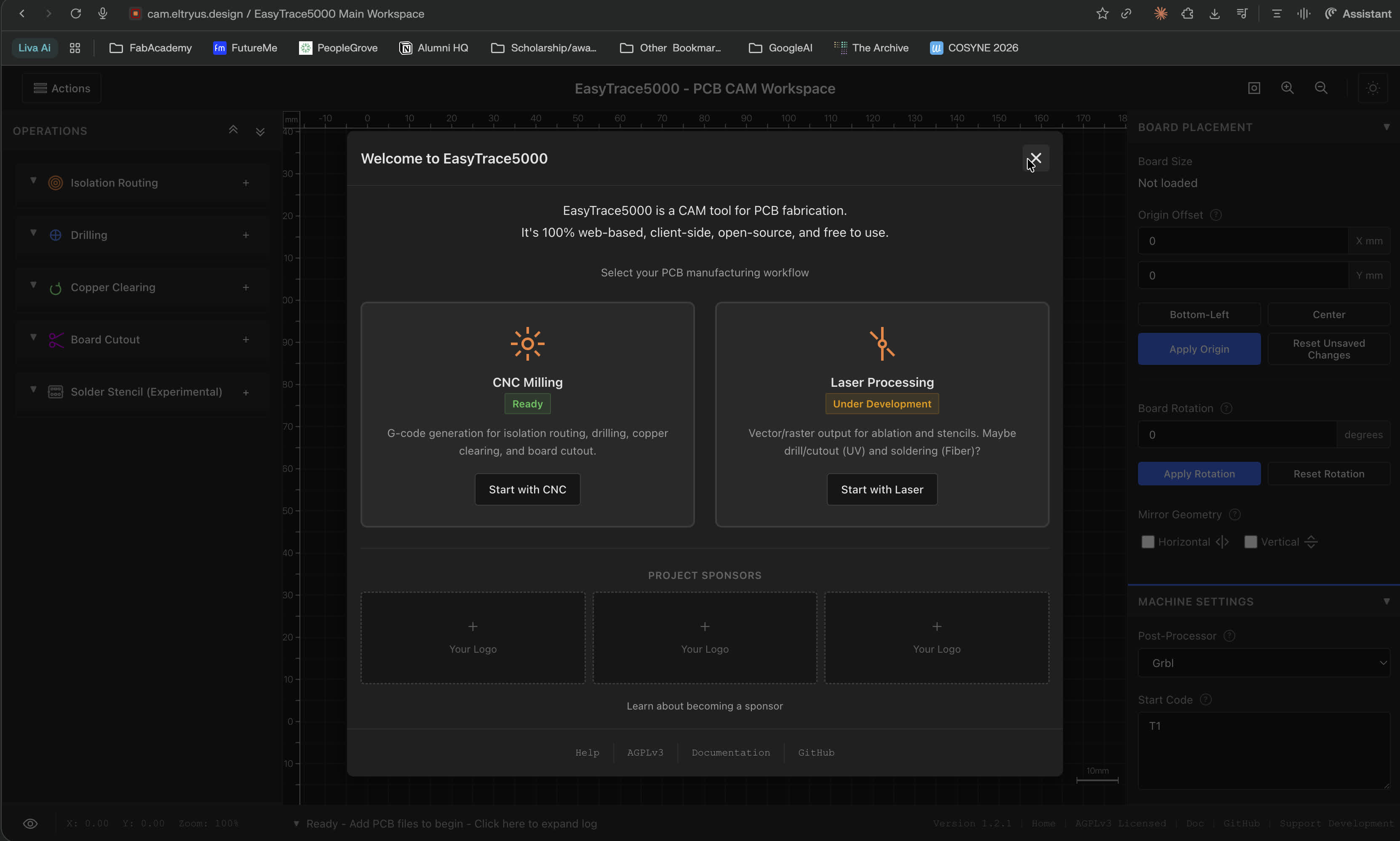
We set up EasyTrace5000 with a V-bit, a starting tool diameter of 0.249 mm, and a cut depth of -0.04 mm. Post-processor was Grbl. We ran a line test at 0.3, 0.2, 0.1 and 0.01 mm widths and spacings.
For the line test, we used the file that is built into EasyTrace5000 rather than designing a new one ourselves.
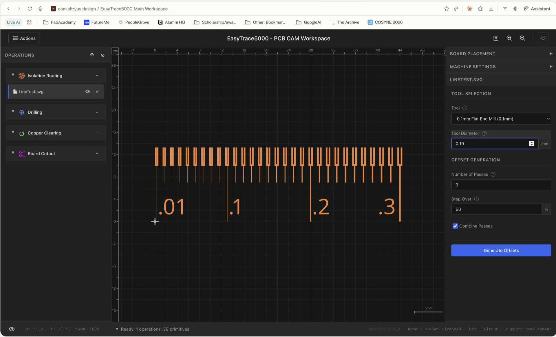
The 0.2 mm lines came out clean. The 0.1 mm lines came out as a mess of merged copper. The 0.01 mm lines just did not exist.
The tool diameter alone, 0.249 mm, is bigger than the 0.01 mm spacing we asked for.
The machine could have the resolution to create finer traces but usually the interaction between the cutting tool and the copper or later when deburring that leads to smaller traces being snatched off the board.
The rules you set in KiCad are downstream of the bit you put in the spindle.
The other thing that surprised me was how much of the process is just making the board flat enough for hundredths of a millimeter to matter. We used double-sided tape on a sacrificial bed for fixturing.
For zeroing Z we used the probing function in Candle. You clip one wire to the V-bit, another to the copper, and lower the spindle until the bit touches the surface. The moment current flows through that little circuit, the machine sets that as zero. It is a clever and very cheap trick.

We also generated a height map of the board surface so that EasyTrace5000 could adjust the toolpath as it cut. That is the only reason a fixed -0.04 mm cut depth gives you a consistent result across a board that is never perfectly flat.
The rules we ended up writing down for our lab were 0.2 mm minimum trace width and 0.2 mm minimum spacing. Anything finer than that has to go out.
Which is exactly what Part 2 was about.
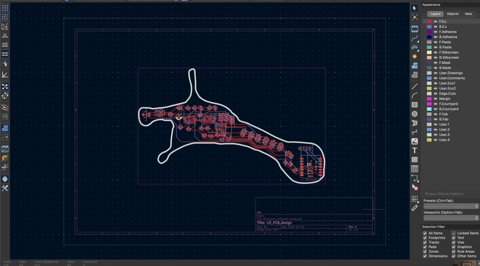
The neuron board I designed in Week 6 turned out to be the perfect case for sending out. Its trace widths and spacings sit below our 0.2 mm limit, and the density of the routing meant that the chance of something going wrong over a full milled board was very high. So we used it as our test case for the board-house workflow.
We re-opened the design in KiCad and edited the design rules to match what JLCPCB advertises. Then we re-ran the DRC to make sure nothing was newly broken. The interesting realization here was that DRC is not one fixed thing. It is parameterized by who is making the board.
In-house DRC and board-house DRC are two different rule sets pointed at the same design. A design is only valid relative to a specific manufacturer.
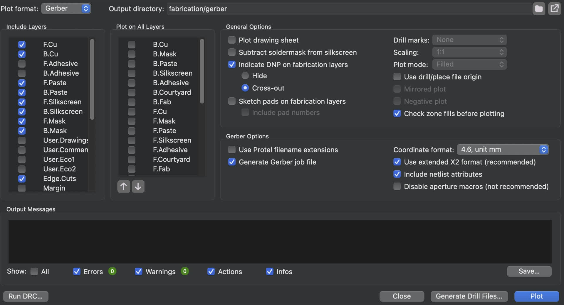
Then we exported the manufacturing files. Gerbers for each copper layer, plus solder mask, silk screen and outline, through File > Fabrication Outputs > Gerbers. Then the drill file separately through File > Fabrication Outputs > Drill Files.
We walked the design through the JLCPCB web flow. Drag-and-drop the Gerber zip. Look at their rendered preview to make sure the layers line up. Pick the manufacturing options like board thickness, copper weight, solder mask color and surface finish. Let their own DRC run. Then look at the price and lead time.
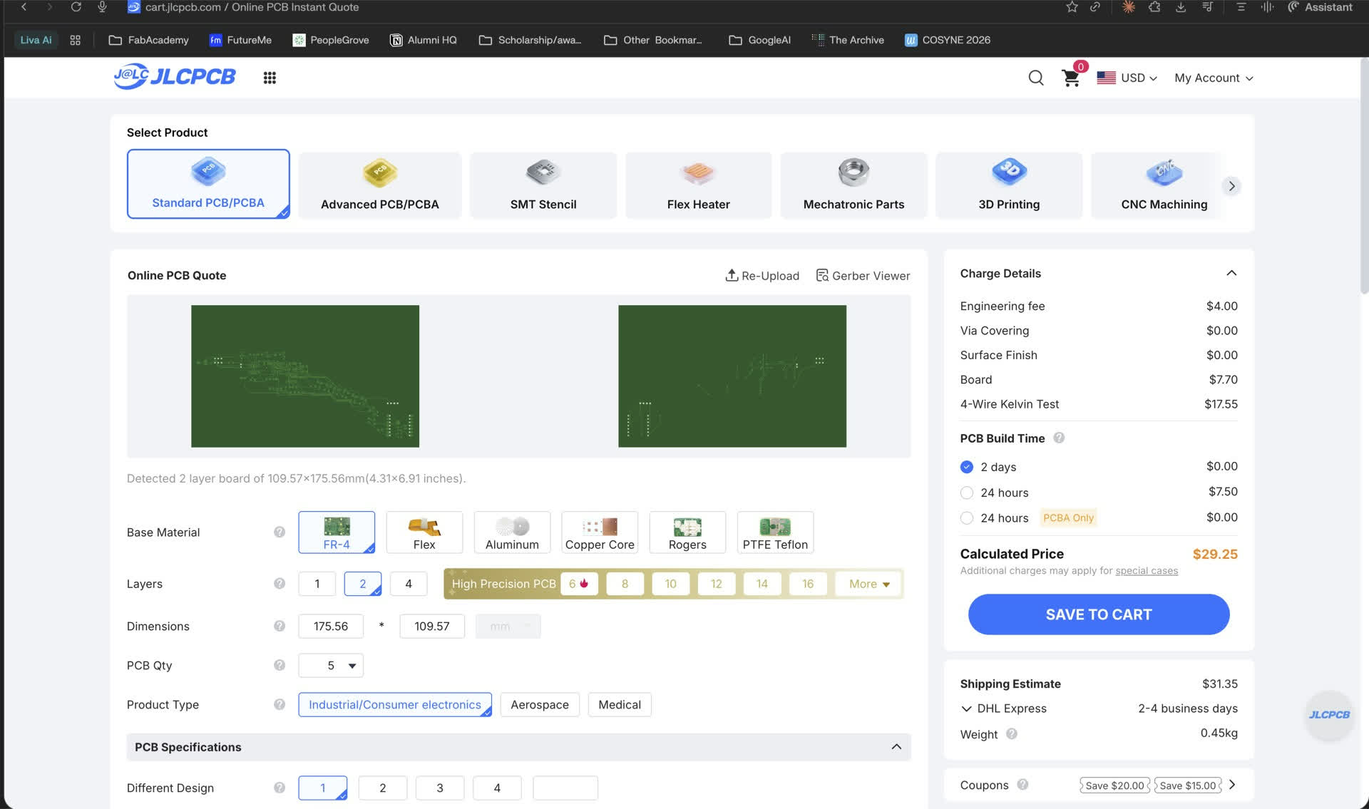
We stopped at the documentation step rather than actually placing the order, but going through it end-to-end made the difference between in-house and board house feel concrete.
In-house is minutes and free, but capped at 0.2 mm features and a single layer. A board house takes days to weeks and costs money, but you get fine-pitch parts, multi-layer routing, plated vias, solder mask and silk screen. Most of those things can’t be done well using thee equipment we have.
Board houses could be the way to go for a more polished board for my final project glasses PCB.
Learnings
Coming into this week, my mental model of a PCB was basically “the green thing inside electronics with the components on it.” I had used breadboards before and I knew you could buy custom boards from somewhere, but actually making one yourself felt like a black box.
Week 6 taught me how to design a circuit in KiCad, but a KiCad file is just a drawing on a screen. This week was about closing the gap between that drawing and a real, soldered, working board sitting on my desk.
This section is for someone like me a few weeks ago: someone who has poked at an Arduino, maybe stuck some jumper wires into a breadboard, but has never milled, etched, or soldered a board of their own.
Some of what is below came from the global session led by Quentin Bolsée, Isaak Freeman, and Sean Hickey (with Neil chiming in throughout), some came from the Fab Academy class page, and the rest came from some research afterwards to make things actually click.
An important poem to keep in mind:
Etching vs Machining, and Why We Mill in Fab Labs
The classic way to make a PCB is chemical etching. You start with a copper-clad board, mask off the copper you want to keep with some kind of resist, and dunk the board in a chemical bath that eats the rest.
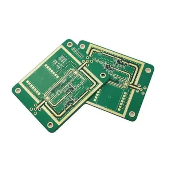
Ferric chloride, cupric chloride, and ammonium persulfate are the usual suspects. This is how essentially every commercial PCB you have ever touched was made.
The catch is the chemistry. Neil pointed out that one square meter of circuit board produces roughly a cubic meter of chemical waste.
The etchants are toxic, you need to dispose of them carefully, and you have to keep all that stuff around the lab. Not exactly the Fab Academy spirit.
So instead of dissolving copper, in the lab we machine it away. We use a tiny CNC mill with a very small bit and we cut grooves around the traces we want to keep. The “waste” is just copper dust, which is a much friendlier thing to clean up.
The trade-off is resolution: we cannot get the same hair-thin traces an etched or lithographic board can, but for the kind of microcontroller boards we are making it is more than enough.
Other Ways You Can Make a Board
Etching and milling are the two big categories, but the session also walked through a bunch of other ways people make PCBs in Fab Labs.
Vinyl cutters can cut copper tape into traces. It is fiddly and takes practice, but it is great for one-off circuits and especially for flex circuits where you do not want a rigid board.
Laser engraving is, according to the session, slowly replacing milling in some labs. A fiber laser or a 300nm UV laser can cleanly remove copper. The UV ones are very new but apparently produce stunning results, while the 1-micron lasers work but leave a rougher edge.
There is also a technique called Laser-Induced Graphene (LIG), where the laser literally converts a polymer into conductive graphene traces. The session mentioned that one of the Fab Labs published a paper on this, which was a fun reminder that the network is doing real research, not just teaching.
Conductive ink printing exists but is not really mainstream in Fab Labs yet.
And finally, for anything beyond a handful of boards, the realistic option is to send your design to a board house.
JLCPCB and PCBWay are the cheap-and-fast Chinese services everyone seems to use, and OSH Park and Aisler are the alternatives if you want something closer to home.

What the Boards Are Actually Made Of
I had no idea before this week that “PCB” was a category, not a single material. The board itself is some kind of insulating substrate with a copper layer bonded on top, and there are a few options.
FR4 is not the green color itself. FR4 is the epoxy resin and glass-fiber substrate inside the board, and bare FR4 is more like a pale, almost transparent matte yellow material. The green layer on a lot of commercial PCBs is usually solder mask added on top of the copper and substrate. FR4 is still bad news to mill in the lab because the glass fibers are nasty to inhale and tear up tool bits.
FR1 is what we use in the lab. It is copper bonded to a phenolic paper substrate. Way safer to machine, no glass dust, and perfectly fine for our purposes.
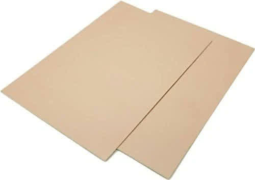
There is also copper tape, which is exactly what it sounds like and is handy for quick prototypes, and flex materials like Kapton and Pyralux for flexible circuits.
Copper itself comes in different thicknesses, measured oddly in ounces per square foot. 0.5oz is about 17.5 microns, 1oz is 35 microns, and 2oz is 70 microns.
When you mill a board you are only cutting through this very thin copper layer, so the depth of cut is tiny. Get it wrong and you either do not break through the copper at all, or you dig way too deep into the substrate.
The Milling Machine Itself
The mills used for PCBs are not the big shopbot-style machines from Week 7. They are small desktop CNC mills like the Lunyee Neil mentioned. Same idea as a big CNC, just shrunk down.
Neil also pointed out that the spindles these things ship with usually have too much runout (basically, the bit wobbles instead of spinning perfectly centered on the spindle's axis, causing it to create uneven traces), which is why he upgrades the spindles in his lab.
For the actual cutting you have a few choices of bit. Your "standard" option is whatever one you have access to. Cheap v-bit are the closest to a "standard" since they are widely available and accessible.
V-bits are conical, and have fragile tips. The width of cut depends on how deep you push them, so you can dial the trace width by changing the Z, so as the v-bit wears off, you could adjust the depth or width and still be able to use.
Honestly though, you are probably better off using another v-bit. They are noisier than straight bits but much more forgiving.
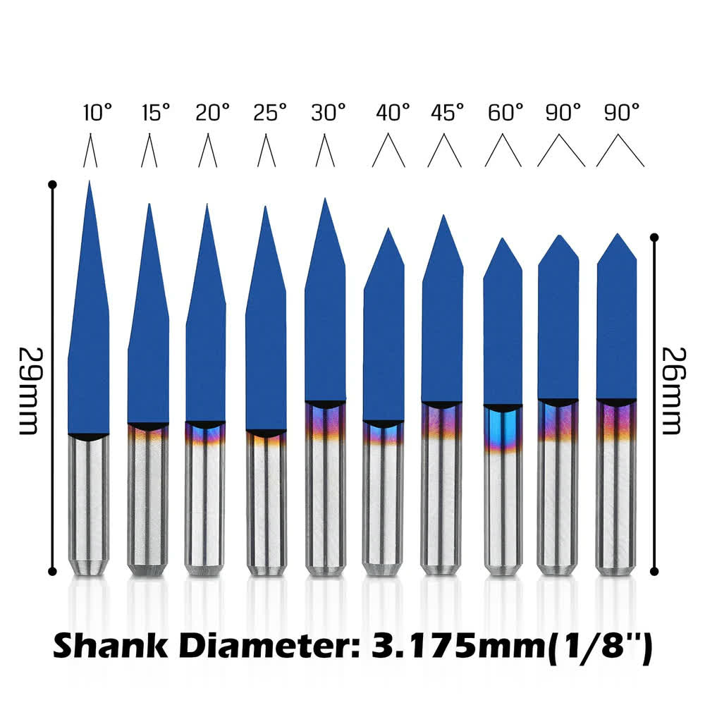
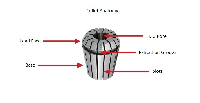
The collet, which is the part of the spindle that grips and holds the bit in place, is usually 1/8" on these machines, which is 3.175 mm.
Holding the Board Down and Finding Zero
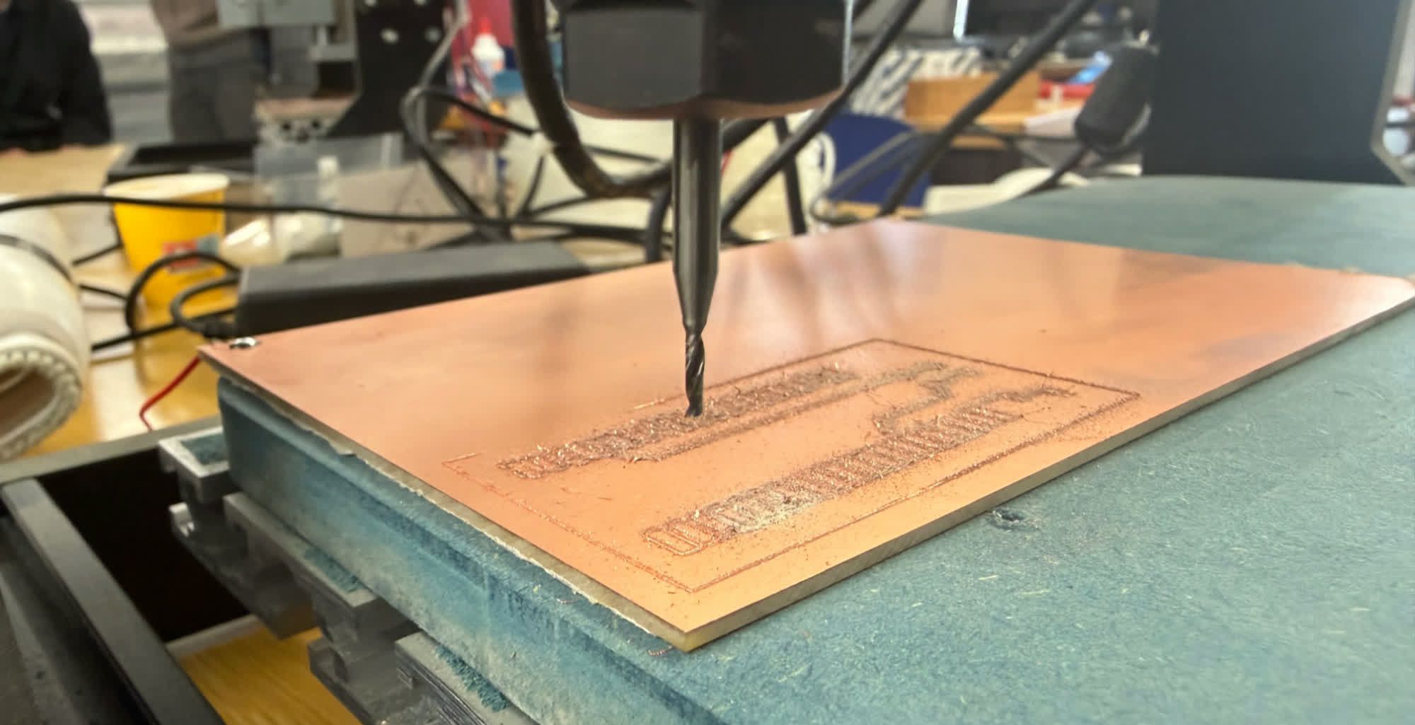
Holding a PCB blank is a different problem than holding a piece of plywood. The board has to be dead flat across the whole cutting area, because the depth of cut is measured in fractions of a millimeter.
If the board even slightly bows, parts of your traces will be too deep and parts will not cut through at all, and you will end up with a board where some traces work and some are still shorted to the copper around them.
Double-sided tape on a flat sacrificial surface is the simple solution and it works well. The sacrificial surface gets cut into over time and you swap it out occasionally.
Zeroing the Z axis is the part that surprised me the most. You do not get fancy probes on these little machines, you just touch the bit to the surface and call that zero.
Neil showed a clever way: loosen the collet so the bit can slide, lower the spindle until the bit is sitting on the board, then retighten. Because the threads pull the bit slightly upwards as you tighten, you compensate in software by lowering Z by a fraction of a millimeter.
The other trick is the paper feeler: slip a piece of paper between the bit and the board, lower until the paper just gets pinched, then offset by the paper thickness.
The cleanest version of all of this is electrical probing, which is what we ended up using in our lab. You clip one alligator wire to the metal V-bit and the other to the copper of the board, which turns the bit and the copper into the two ends of an open circuit.
Then you tell the controller (Candle, bCNC, or whatever you are using) to slowly jog the spindle down. The moment the bit touches the copper, current flows through that little circuit, the controller sees the contact, stops the motion, and sets that exact Z position as zero.
It is way more repeatable than eyeballing it or pinching paper, and it costs nothing because the wires are the only extra hardware.
For pcb milling we generally rely on the conductivity of the surface, but there are other touch-probes that can measure coordinates on any surface. It's the base concept behind Coordinate Measuring Machines.
The same idea scales up into surface autoleveling. Instead of probing a single point, you have the controller probe a grid of points across the whole board. Each touch records (X, Y, Z), and the software builds a height map of how much the board bows or tilts.
The toolpath is then warped on the fly so that the depth of cut stays the same everywhere, even on a board that is not perfectly flat. This is what saves you when fixturing alone is not enough.
After you finish milling, the board has burrs and copper dust everywhere. You brush off the dust and scrape off the sticking copper lightly with steel wool and then wash it, both to get rid of the dust and to clean off skin oils from your fingers. Skin oil on the copper makes soldering a pain.
Metals generally come with a thin film of oil on top so that they oxidize less.
You need to make sure not to rip the traces.
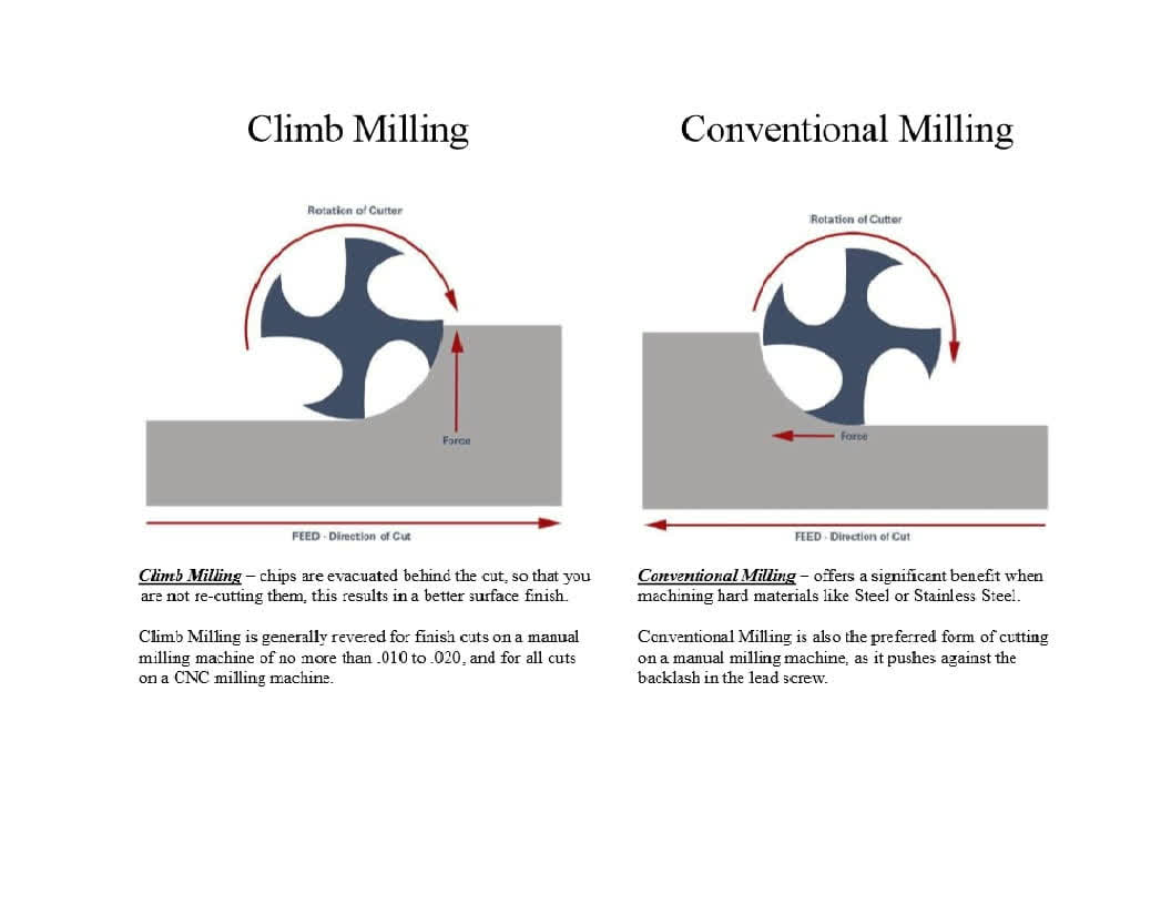
Climb vs Conventional, Round Two
We talked about climb vs conventional milling back in Week 7 with the big CNC. Same thing applies here, just on a smaller scale.
Conventional milling pushes the work into the cutter and is gentler if you are worried about cutting forces.
Climb milling pulls the cutter through the work and gives a cleaner edge but loads up the spindle. On these little desktop machines climb milling is usually preferred because cleanliness matters more than force, and the forces are small anyway.
Design Rules: The Bridge Between KiCad and Reality
In Week 6 we ran “Design Rule Checks” in KiCad without really questioning what those rules were. The rules answer two questions: how thin can a trace be before it falls off or breaks, and how close can two traces be before they short to each other?
The answer is “it depends on how you are making the board.” A real board house can hit something like 5 mil (0.127mm) trace width and spacing without breaking a sweat.
Our in-house mills are more in the 15 mil width / 5 mil spacing region, and even that depends on the bit and the machine. Figuring out what our specific lab can actually do is literally what the group assignment is about: we mill test patterns with traces of decreasing width and spacing and find where it stops working.
The other half of design rules is via stuff. A via is just a hole that connects the top copper layer to the bottom copper layer.
Commercial board houses electroplate the inside of the hole. We cannot do that in the lab, so for in-house boards, vias are either header pins, rivets, or just a piece of wire soldered through the hole.
There is also a slick trick: if you only have a couple of traces that need to cross each other, you can cheat and use a 0-ohm resistor as a one-component “jumper” instead of bothering with a two-sided board.
There are also fancier vias (blind vias that stop in one layer, buried vias hidden in the middle of multilayer boards) but those are firmly board-house territory.
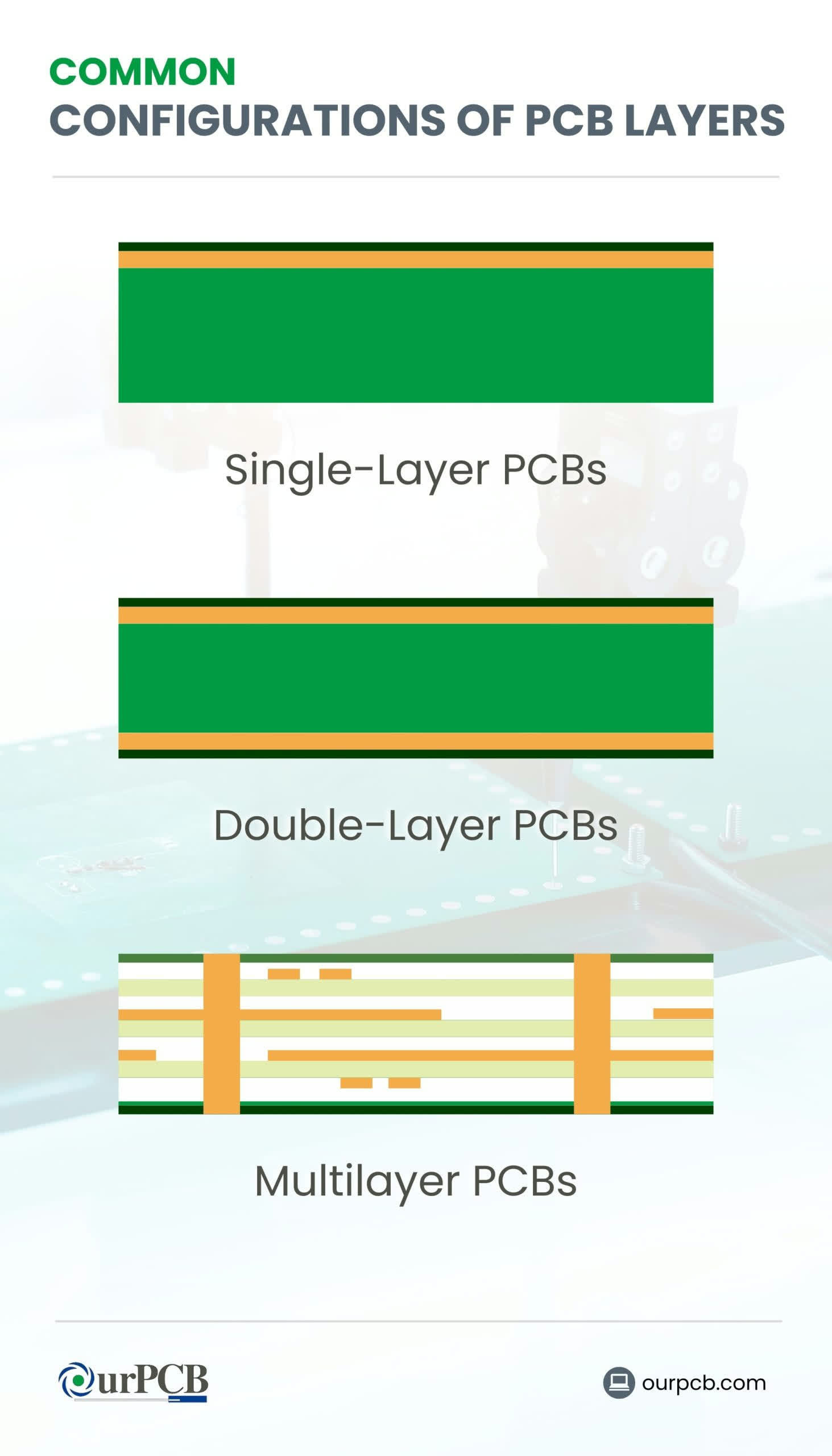
Layers and What They Mean
A board file you send to a board house has more than just the copper traces. You have the mechanical layer that defines the board outline, the drill file for the holes, the solder mask (the colored coating that covers the copper except where you want to solder), and the silk screen (the white text printed on the board).
For in-house production most of this is irrelevant: we just mill the copper. But it is important to understand the layers because the group assignment includes sending a real Gerber to a board house.
Common board configurations are 1-layer (basically what we mostly mill in-house), 2-layer (the bread and butter of board houses), and 4-layer (for anything denser).
From KiCad Files to G-Code
So you have a KiCad design. The mill speaks G-code. Something has to translate between them, and that is what CAM software does. The file formats in the middle are Gerber (RS-274X) for the board-house route, and PNG for some of the lab tools.
mods is the open-source tool the Fab community built. You feed it a PNG of your traces and it spits out a toolpath. Neil expects us to learn it and try it.
Easytrace5000 is a tool Ricardo made because, in his words, he hated mods so much that he made his own.
It exposes parameters like tool diameter, depth, and speed, and importantly it does surface mapping, where it probes the board height in a grid first and adjusts the toolpath so the depth is consistent even on a slightly bowed board.
FlatCAM and pcb2gcode are other open-source Gerber-to-G-code tools. KiCad also has plugins that export directly to board-house-friendly formats, which is what I will use for the group assignment.
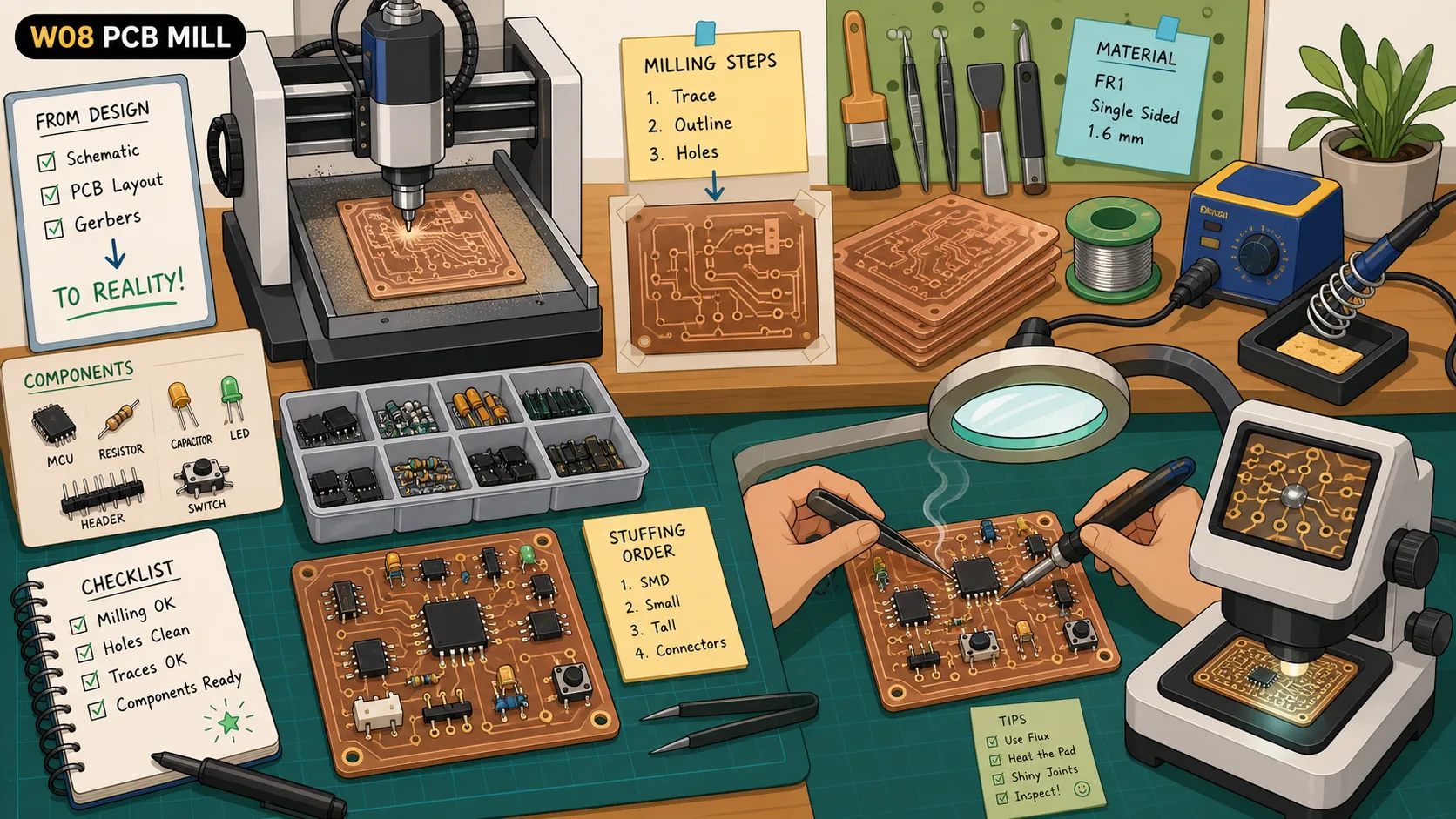
Soldering Components On
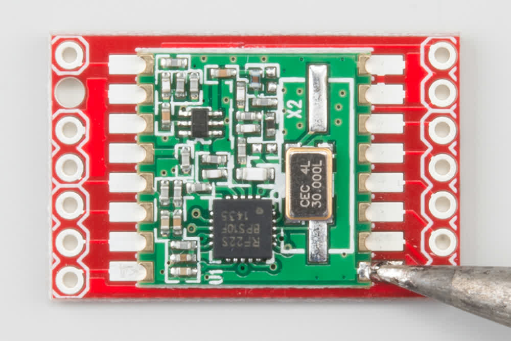
In Week 6 we learned what resistors, capacitors, LEDs, and MOSFETs do. This week we actually attach them to a board. I had soldered through-hole stuff a couple of times before but never SMD, and I was pretty nervous about it.
The fundamentals from the session: keep the iron tip clean and tinned, meaning coated with a thin film of solder. A black, oxidized tip will not transfer heat properly.
Heat the joint, not the solder. You touch the iron to the pad and the leg of the component at the same time, then touch the solder wire to the joint. The solder flows because the joint is hot, not because you melted a blob and dripped it on. This is the part that takes practice.
A good joint looks shiny and concave. A cold joint (dull, blobby, lumpy) is unreliable and you fix it by reflowing it with the iron.
We use lead-free solder, since RoHS is the European regulation that pushed lead out of consumer electronics and the lab follows that.
There is more than one way to actually get solder onto a board.
Hand soldering with an iron is what I will mostly be doing this week, and the trick is to do small components first, then bigger ones, otherwise the bigger ones get in the way.
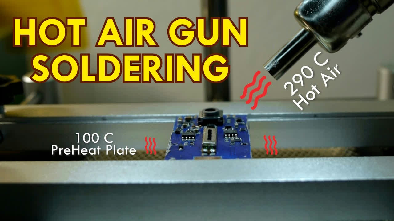
Solder paste with a hot air gun or a hot plate is the fancy way: you apply paste through a stencil, drop the components on top, and heat the whole board until the paste flows. It looks wild the first time you see it, the dull grey paste turning into shiny solder all at once.
Drag soldering is a technique for fine-pitch ICs where you put a generous amount of flux on the pins and then drag a loaded iron tip across them, and surface tension does the work of separating the solder onto each pin.
For getting solder off again you have solder braid (a copper wick that absorbs molten solder), hot air with tweezers for picking off whole components, and vacuum desolderers for through-hole pins.
One thing the session hammered: orientation matters. ICs, diodes, and LEDs have a “right way round.” Get it wrong and at best the component does not work, at worst you fry it. Always check the datasheet for the marking.
And for boards that use modules with castellated pads like the XIAO (the half-moon plated edges), you must solder every castellation you actually care about. Skipping one means an open circuit you will spend an hour debugging.
Why Neil Hates Breadboards
This was probably my favorite part of the session, because I have used breadboards before and I felt slightly attacked. Neil’s case against them:
You need a whole second inventory of through-hole parts, because the Fab Academy SMD components do not fit in a breadboard.
The connections are mechanical, electrically noisy, and unreliable. They work, until they suddenly do not.
There is no documentation, since a jungle of wires is not a circuit diagram and you cannot reproduce it later.
And if you pick the breadboard up and walk across the lab with it, wires fall out.
The Fab Academy answer is that you should design and fabricate a real PCB even for prototyping, and after this week I sort of see why.
Debugging When the Board Does Not Work
The session ended with what to do when (not if) your freshly soldered board refuses to work. The order is roughly:
Look at the board carefully first, because most of the time the problem is visible: a cold joint, a solder bridge between two pins, a missing connection where you forgot to solder a leg.
Reflow anything that looks suspicious. Touching the iron to a sketchy joint and adding a tiny bit more solder fixes a surprising number of bugs.
Double check component values, because a 1k where a 10k should be looks identical but behaves very differently.
Cross check pinouts against the datasheet to make sure you wired the chip the way you thought you did.
Measure the supply voltage with a multimeter, because if the chip is not getting power the rest of the debugging is wasted.
And finally, probe I/O signals with the scope or the logic analyzer to actually see what the pins are doing.
This is essentially the same procedure I use when debugging code: start cheap (look at it), then medium (poke it), then expensive (instrument it). Same instinct, just different tools.
Designing a New, Simpler PCB
For my first ever board, the board I designed in week 6 was too complex for my first board ever. There were a lot of traces, components, and most importantly, I didn’t take into consideration the constraints of the machines available at the lab in my design rules.
Of course, when designing that board, I had some design constraints, but at the time, we didn’t know much about our machines at at the lab (will be talking about our machines in the milling section).
Don’t worry though, I still wanted to simulate how a neuron works on my own PCB board, so I made an altered version of it during the input devices week.
The idea of my redesign was quite simple, a Raspberry Pi PicoW, an LED, and a button.
Quick overview of the Raspberry Pi PicoW
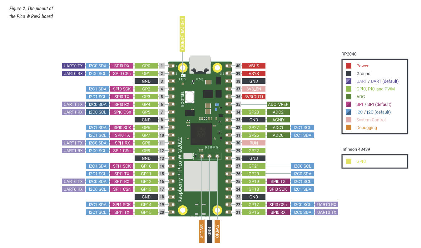
The Raspberry Pi Pico W is a small microcontroller board based on the RP2040 chip, which has a dual-core ARM Cortex-M0+ processor clocked at up to 133 MHz. It comes with 264 KB of SRAM and 2 MB of flash memory.
The "W" in Pico W stands for wireless — it has an Infineon CYW43439 chip onboard that gives it Wi-Fi (2.4 GHz, 802.11n) and Bluetooth 5.2. The regular Pico doesn't have that.
Some of the specs that mattered for my board:
- 26 GPIO pins (3 of which can be used as analogue inputs)
- 16 PWM channels
- 2x SPI, 2x I2C, 2x UART
- Runs on 3.3V logic, with an input range of 1.8–5.5V through VSYS
- Can be programmed over USB with MicroPython, C/C++, or CircuitPython
- 51 × 21 mm in size
For my board I connected an external LED and a button to the Pico W’s GPIO pins. The Pico W already has a built-in LED (wired through the Wi-Fi chip on WL_GPIO0), but using external components was the whole point of this week.
Here's a link to its datasheet.
The Design Process
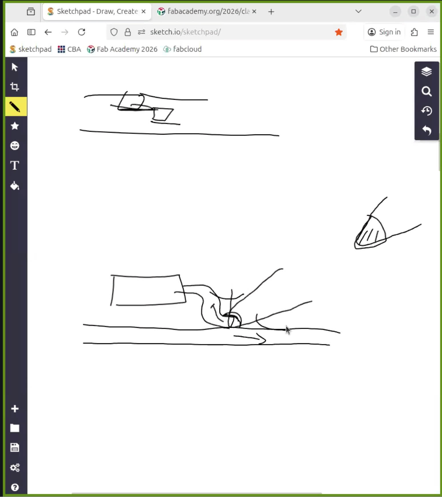
As always, it starts in the schematic mode in Kicad. I added all the components I needed, and started connecting them, since this was quite simple, connecting everything was very straight forward.
Don’t forget to place your PWR_FLAG and NO_CONNECT symbols in their appropriate places and run your electrical rules check.
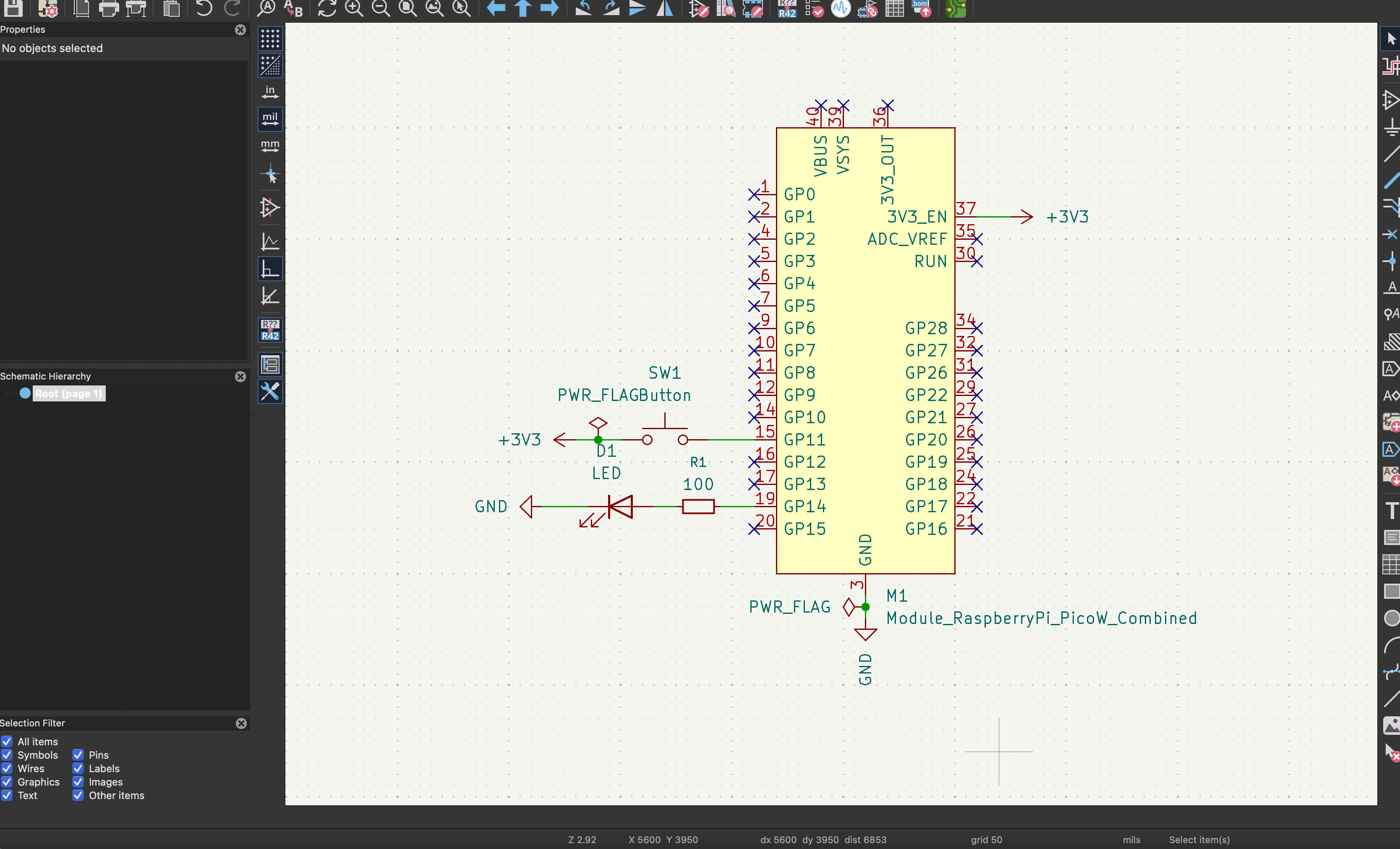
Always remember here is the correct direction of the anode and cathode on an LED, very simple, but important to be correct with that since with other components, like the LED, the wrong connection WILL COST YOU :D

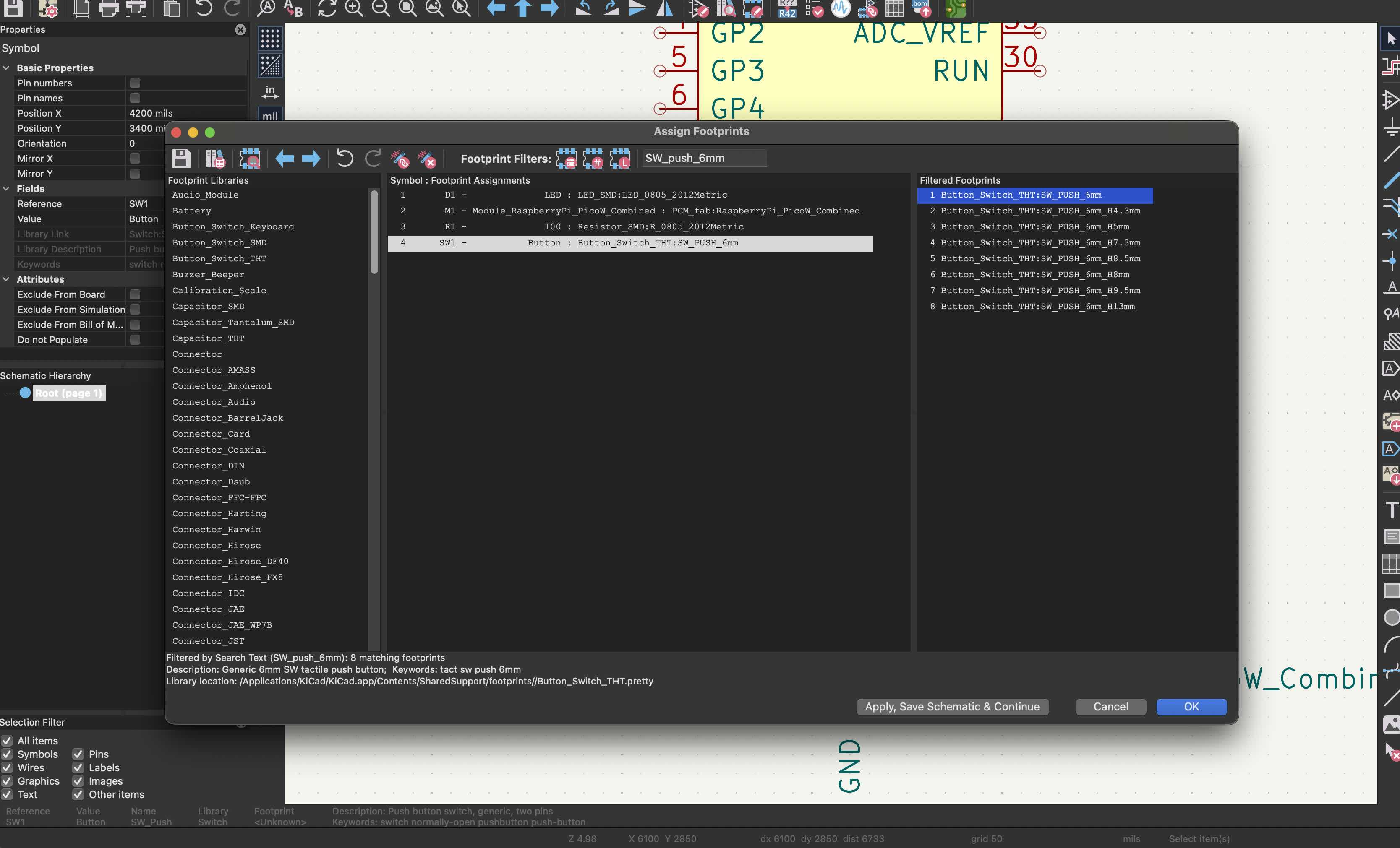
Then, I made sure that each component had a footprint assigned to it by going to Tools > Assign Footprint, which will be important when updating our PCB from the schematic.
Then, I updated my PCB from the schematic (the import was successful, sometimes if you haven’t set up the schematic right or forgot to assign footprints, some components might not be imported).
In my design, I created a ground pour, making the rest of the copper in the board act become the ground. Don’t forget that the grounds throughout all your board should be connected.
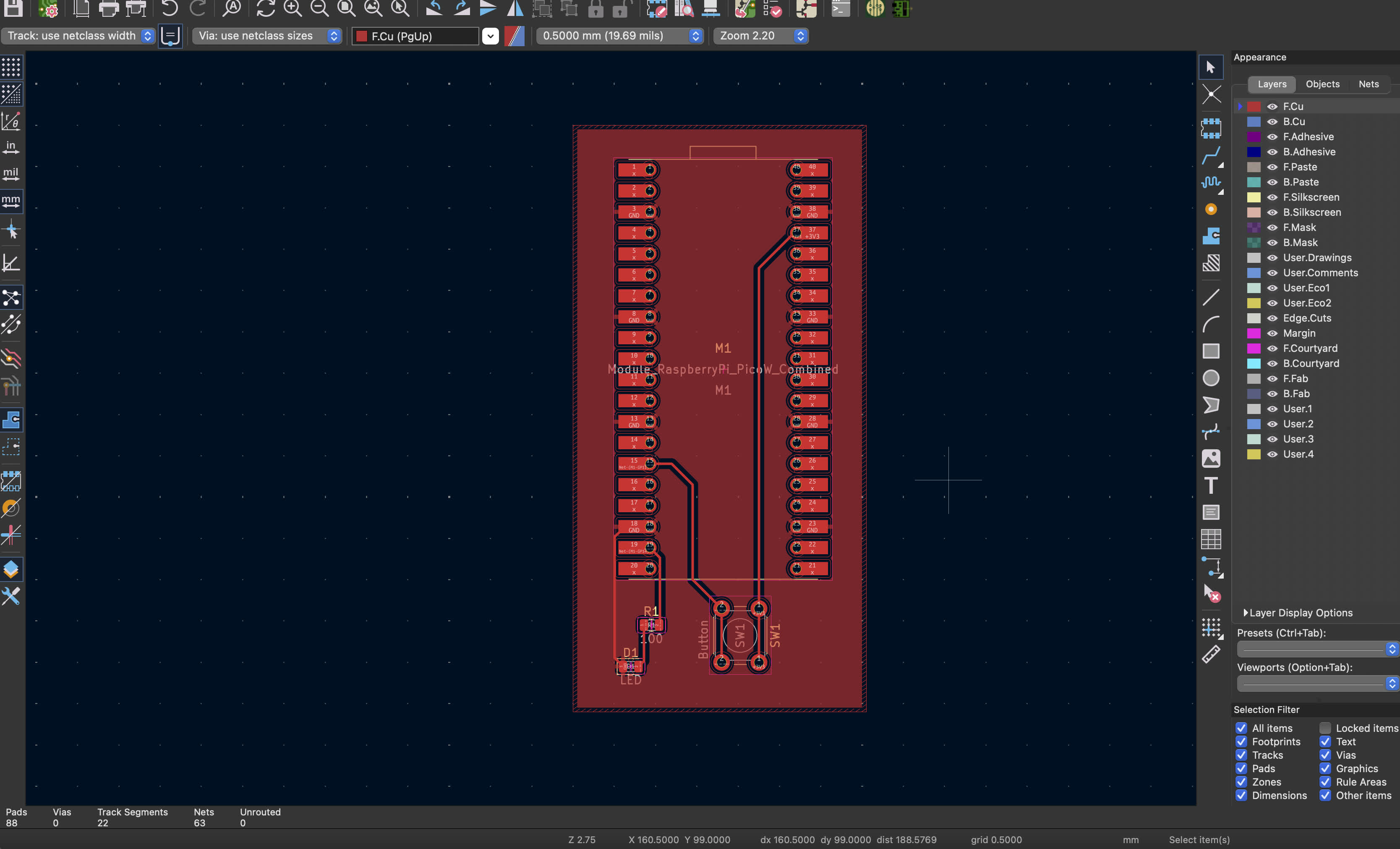
To do that, choose the copper zone tool.

Press on your workspace, and from the pop-up choose GND and ensure you have the front copper layer selected.
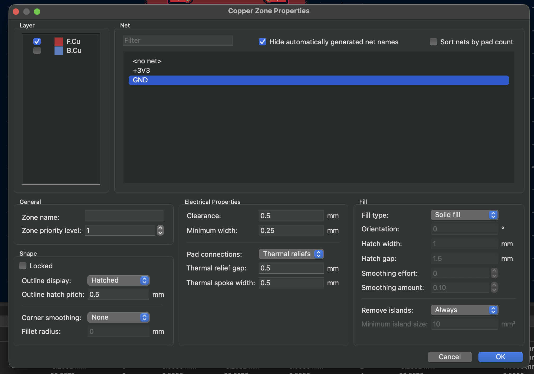
Then, your cursor will be a tool to draw the copper zone, so draw it around your components, and then press “B” or fill the copper zone.
Also, of course, don’t forget to select your edge.cuts layer from the right panel and draw the shape of your board.
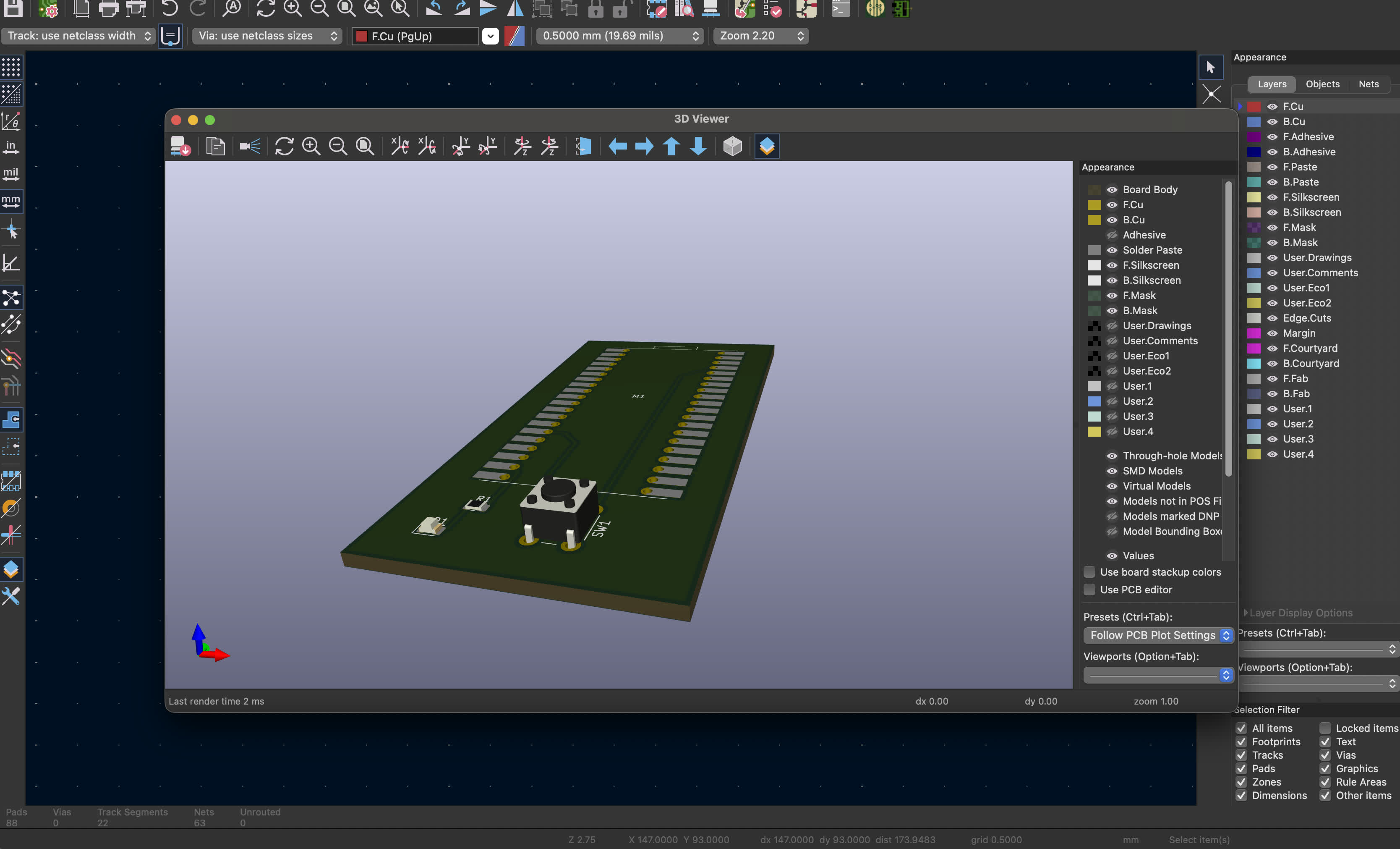
If you set up everything correctly and have 3D models associated with your footprints, you go to View > 3D Viewer.
To prepare for milling, you need to export the files by going to Files > Fabrication Output (not export) > Gerbers, and since I will be using EasyTrace5000 for generating the G_Code, I selected use Protel filename extension.
Don’t forgot to only select the layers you’ll be milling :)
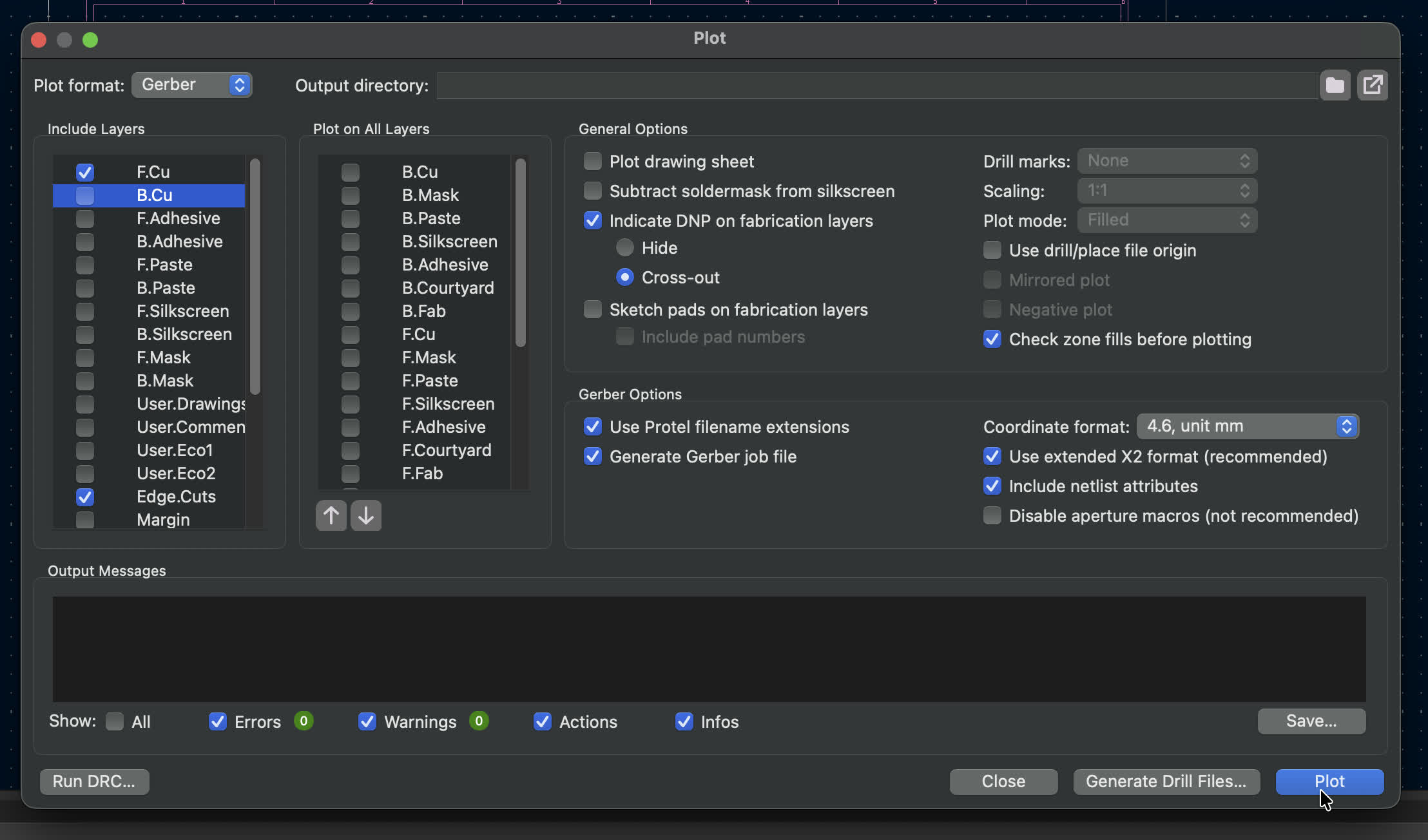
if you had an through-holes, you’d generate drill files too, but for this board, I just pressed plot, and got my files.
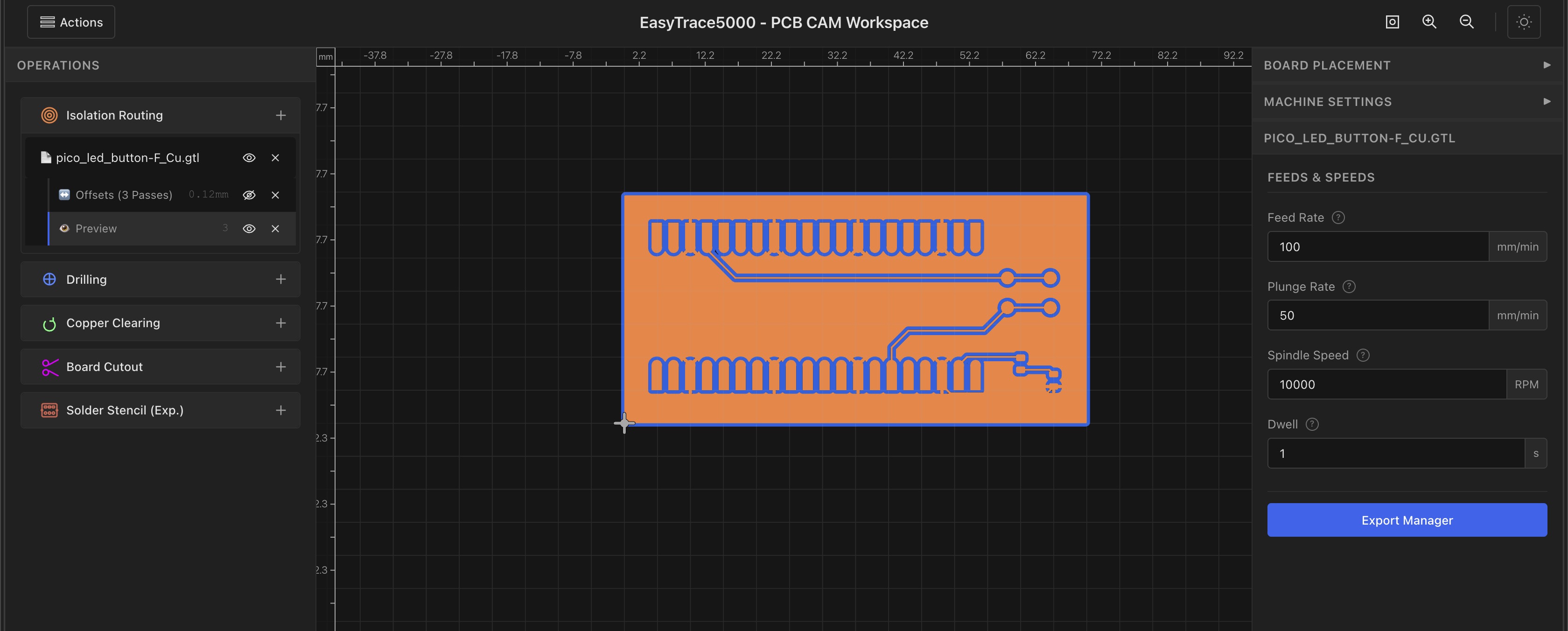
Then, it was time to prepare the g-code on EasyTrace5000, so I started by dragging and dropping my files and setting the bottom left corner as the origin.
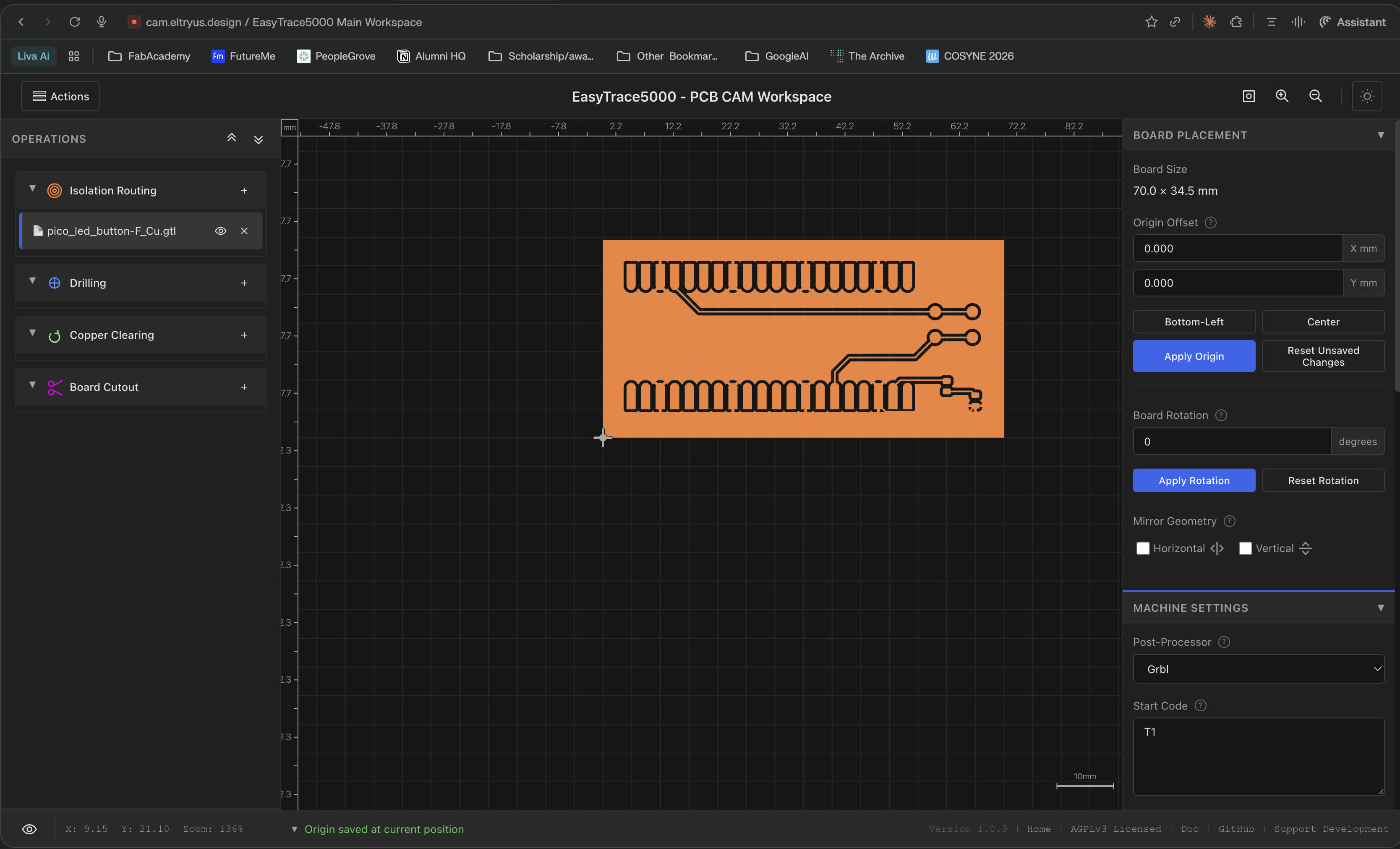
Through our group assignment, we figured that for a brand-new vbit, the tool diameter would be 0.249 mm, the cut depth is -0.04 mm, and you’d do 2-3 passes for the isolation routing.
Those values of 0.249 mm and -0.04 mm were figured out empirically through the group assignment — we ran test cuts, looked at the results, and landed on the combination that gave clean isolation. With EasyTrace5000 you just enter those numbers directly, so there's no math behind them, it's trial and error.
But if you actually want to calculate this properly, MODS (the MIT tool) does exactly that. You only give it two things: the v-bit angle and the tip diameter. From those two inputs alone, it calculates both the cut width and the cut depth for you.
For example, we entered a 20° v-bit with a tip diameter of 0.1 mm. MODS gave us a cut depth of 0.1001 mm and a cut width of 0.1353 mm. Here's how it gets there:
Since the v-bit is conical, the groove it makes is V-shaped. The deeper you push it, the wider the groove gets at the surface. The thing MODS needs to figure out is: how deep does the bit need to go to fully cut through the copper layer?
Standard PCB copper (1 oz) is about 0.035 mm thick. The v-bit enters from the top and its angled sides cut through the copper as it goes deeper. The steeper the angle, the less depth you need to clear the same amount of copper. The shallower the angle, the deeper you have to go. The formula for that is:
cut depth = copper thickness / (2 × tan(angle / 2))
With our 20° v-bit:
cut depth = 0.035 / (2 × tan(10°))
cut depth = 0.035 / (2 × 0.1763)
cut depth = 0.035 / 0.3527
cut depth = 0.0992 mm
That's basically 0.1001 mm (the small difference is just rounding in MODS).
Once you have the depth, the cut width follows from the cone geometry:
cut width = tip diameter + 2 × cut depth × tan(angle / 2)
cut width = 0.1 + 2 × 0.1001 × tan(10°)
cut width = 0.1 + 0.2002 × 0.1763
cut width = 0.1 + 0.0353
cut width = 0.1353 mm
Which is the same as just adding the copper thickness to the tip diameter: 0.1 + 0.035 = 0.135 mm. That makes sense — the groove at the surface is wider than the tip by exactly how much copper the angled sides had to cut through.
A disclaimer about the math: MODS doesn't take into account real-world variables like the wearing of the v-bit and rigidity + squishiness of the double-sided tape, so you might just need to take them into account as you use the v-bit.
If it just scratch the surface/doesn't cut actual traces, you should make it go deeper.
For the board outline, we will be using a 1.5 mm flat-end mill, so we set that up on EasyTrace5000 too, and press on the export manager to get the g-code.
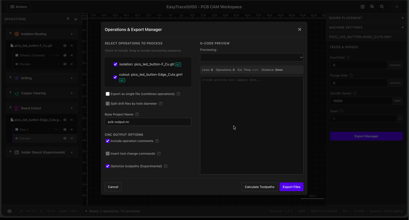
Then, using NCViewer, you could check out the exported g-code and simulate how the machine would behave.
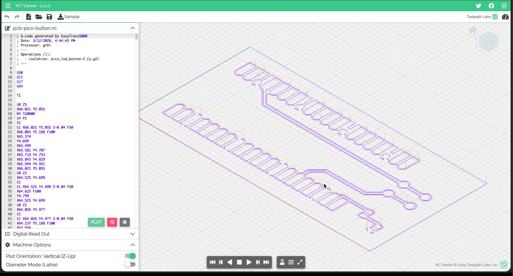
G0 = rapid move. The machine moves to a position as fast as it can without cutting. Used to reposition between cuts.
G1 = linear move at a set feed rate. This is the one that actually does the cutting, moving the bit along a straight line at a controlled speed.
G2 / G3 = clockwise and counterclockwise arc moves. These let the machine cut real curves instead of approximating them with lots of tiny G1 line segments. That is one of the nice things EasyTrace5000 can output, because it keeps the toolpath smoother and avoids the hundreds of tiny linear segments the other CAMs produce and all the problems they bring.
M3 = start the spindle. Usually followed by an S value for speed, like M3 S1000 to spin at 1000 RPM.
M5 = stop the spindle. You call this at the end of a job or before a tool change.
G4 P1 = pause for 1 second. Gives the spindle time to get up to speed before it starts cutting.
X0 Y0 = returns the machine to where the program started.
Now, it is time to talk about milling the board.
Milling the PCB
For milling, we need a CAM software to control and setup our machine, a popular choice is Candle. It has a pretty useful height-map feature built in (will talk about it in a second).
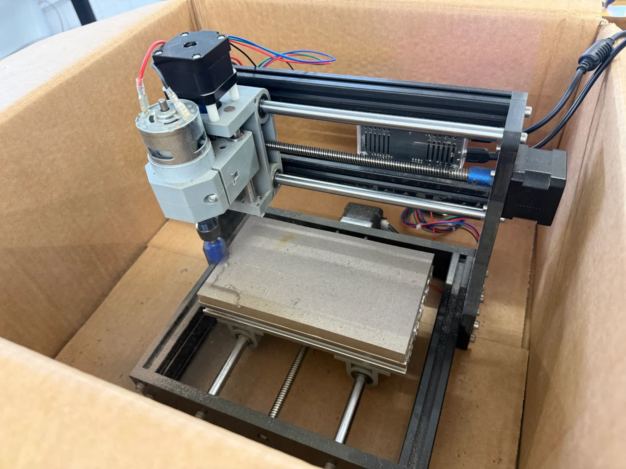
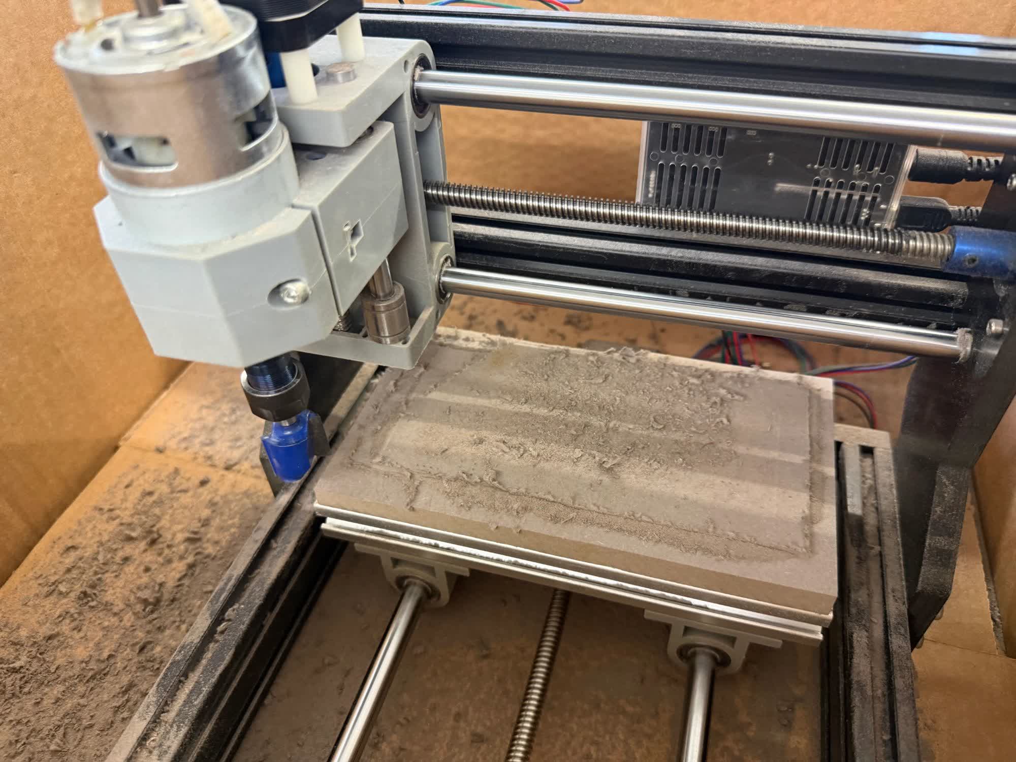
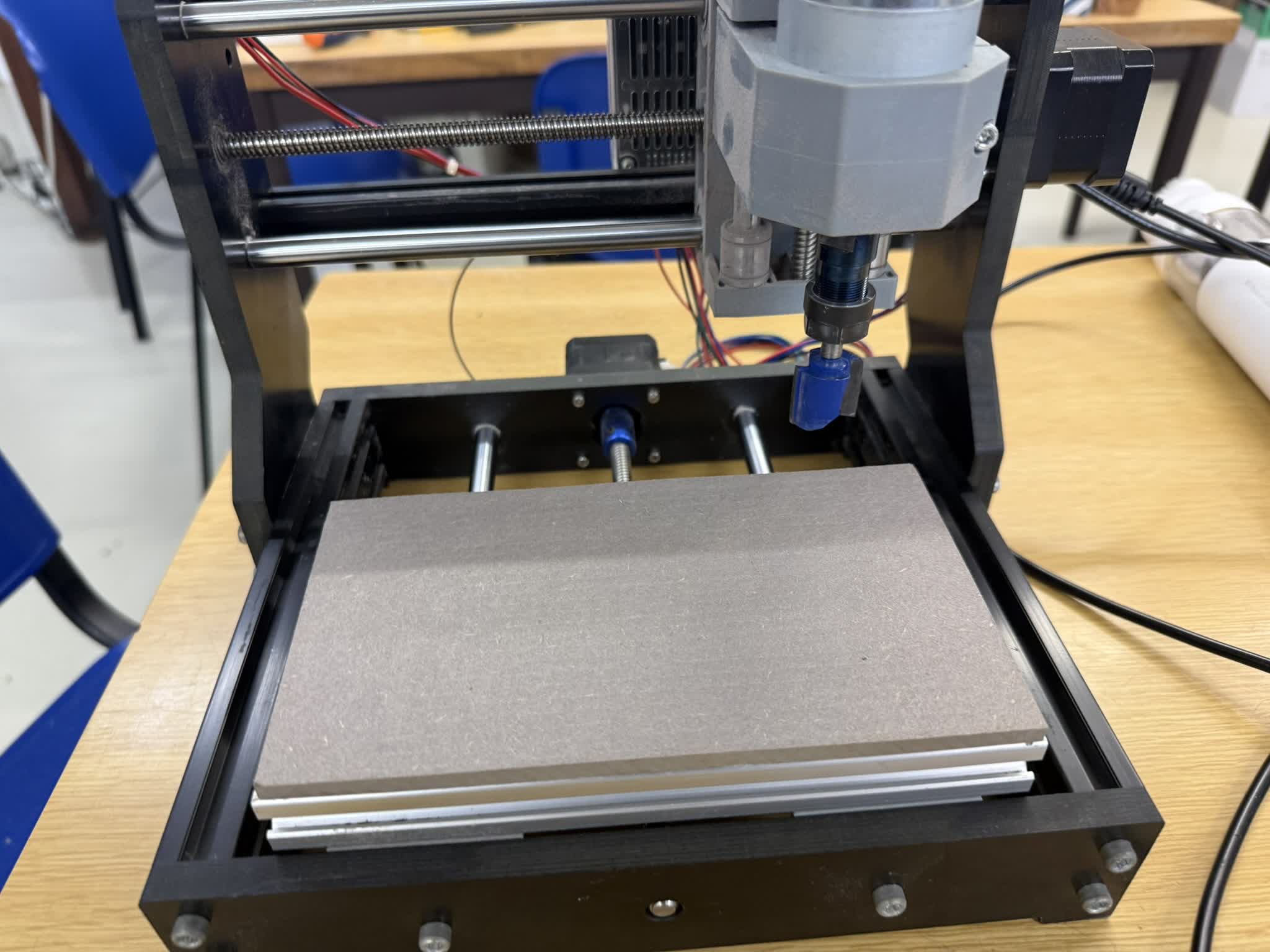
But before getting into that, we need to ensure that the MDF spoil-board of our machine, where we will fixture the copper board, is leveled properly. Usually, you don’t have to worry about this, but our spoilboard wasn’t very flat due to previous use :)
To do that, we need to cut through it MDF with a special spindle, a spoilboard cutter, and it needed a different collet (I used a 6mm) that the mills we’d use for milling our PCB.
I remove the copper board on the MDF and put the whole machine in a box so all the dust and wood won’t fly around. Credit to Daniel, last year’s student at the lab for the inspiration for the technique.
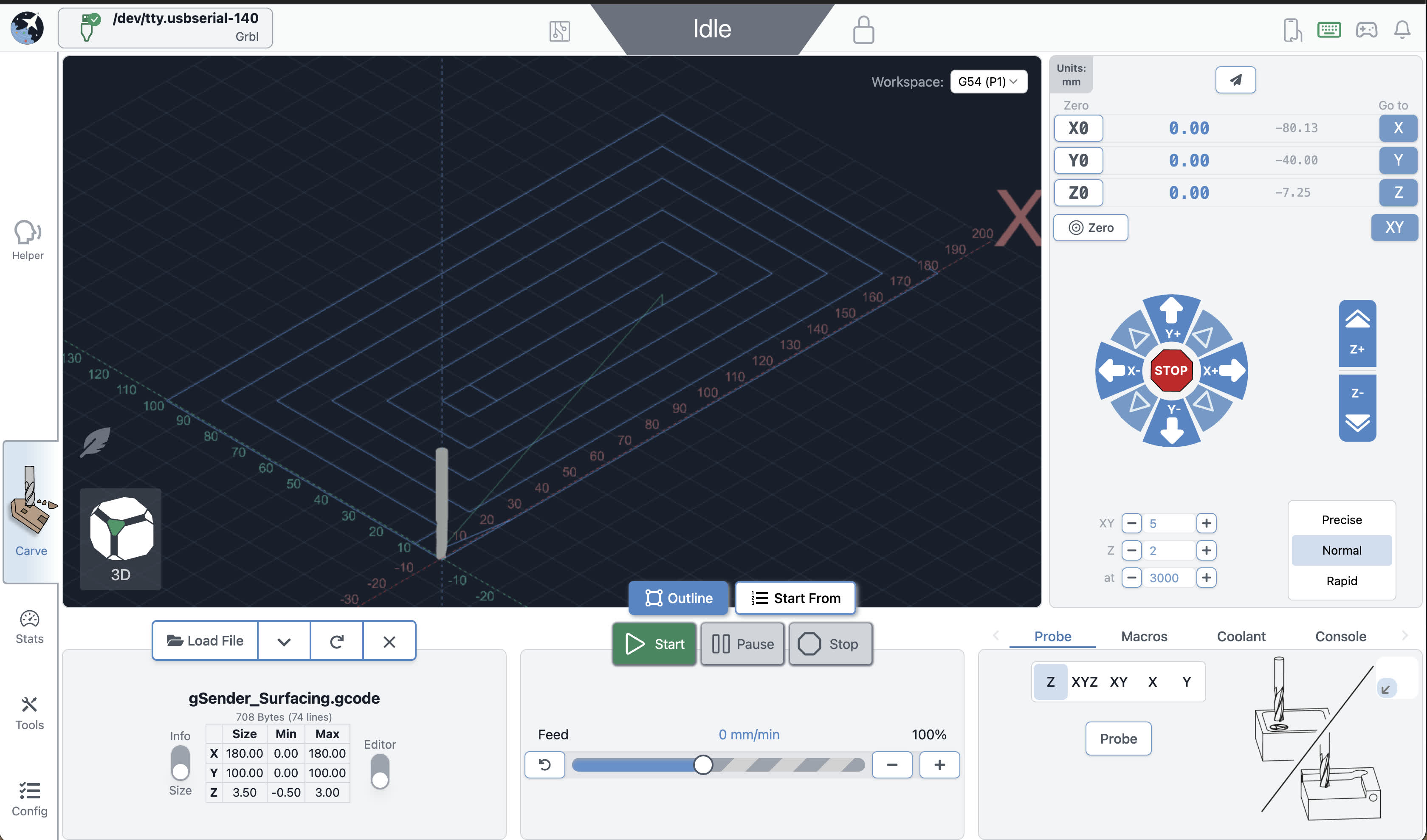
Then, using G-sender’s surfacing tool, I prepared a g-code file with a cutting pattern to level the surface.
Here’s where the biggest problem of the week happens.
Problems Faced While Leveling the Spoilboard
It all boils down to me following Daniel’s images on his documentation, I initially thought his numbers were right, but apparently, the images didn’t have the final parameters he used for the settings of the surfacing tools.
I went through a couple of iterations of the numbers till I nailed it. The issue was that each time while cutting it is going a bit too deep and the spindle can’t handle cutting that much at once, but until I figured that out, I cut the board at multiple spots, making it look like this :(
Since all my failed experiments led to different parts of the spoilboard with different lengths, I needed to run the fixed program a couple of times to get everything almost leveled that a final run of the program would run smoothly.
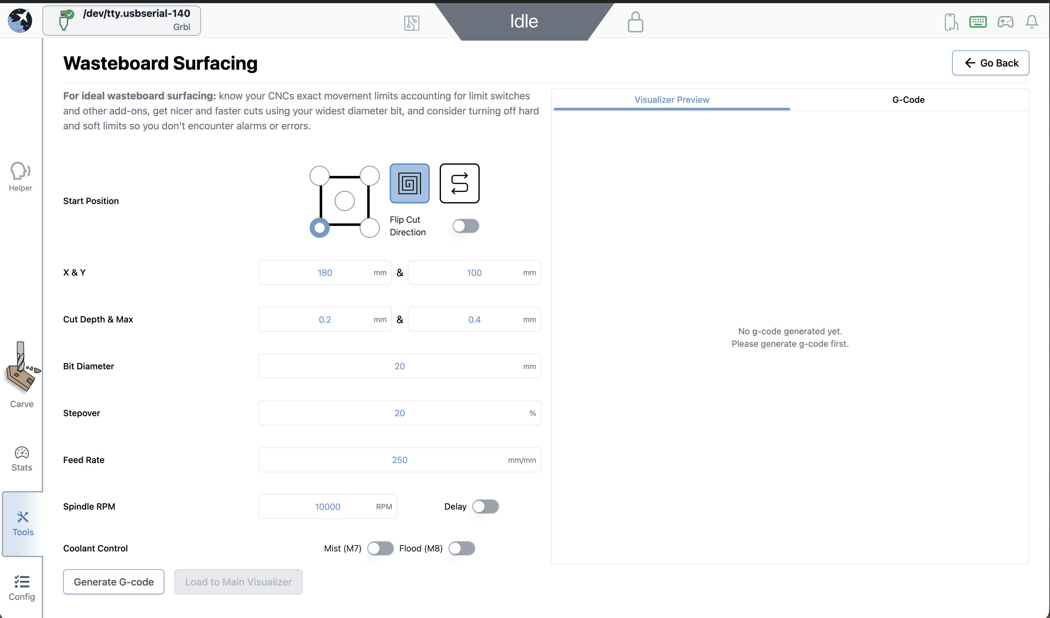
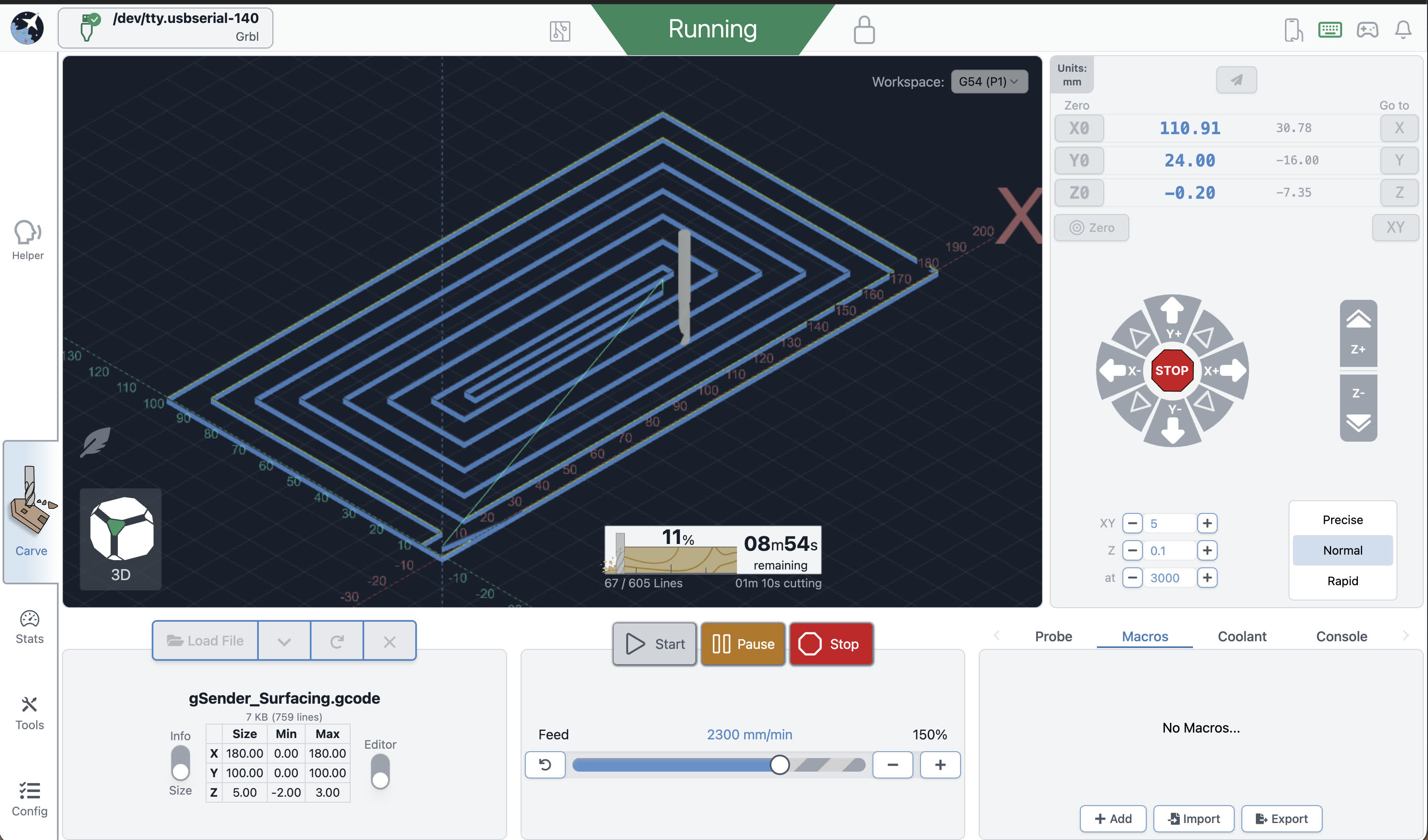
The images above are of the fixed parameters and noticeably you could see how many more passes it is going through. Here’s how the final MDF looked like.
Milling the Copper
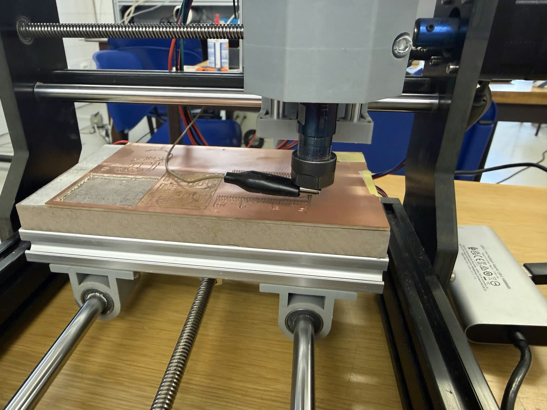
The first step was to fixture the copper board. We had standard FR1 copper boards, so we used double-sided tape to hold it in place on the MDF.
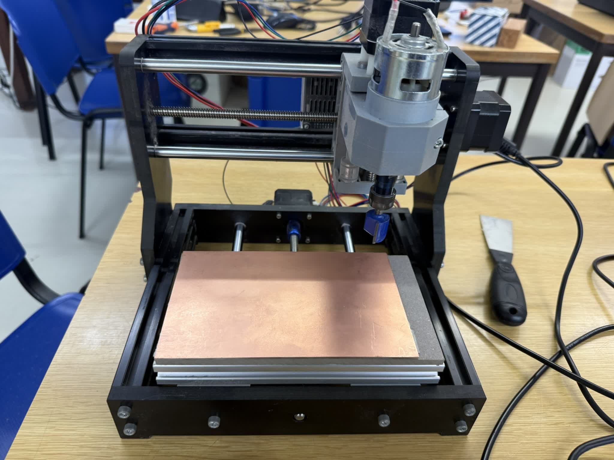
Then, I changed our collet to a 1/8th in collet, which fits our vbits and flat-end mills for drilling and cutting the board.
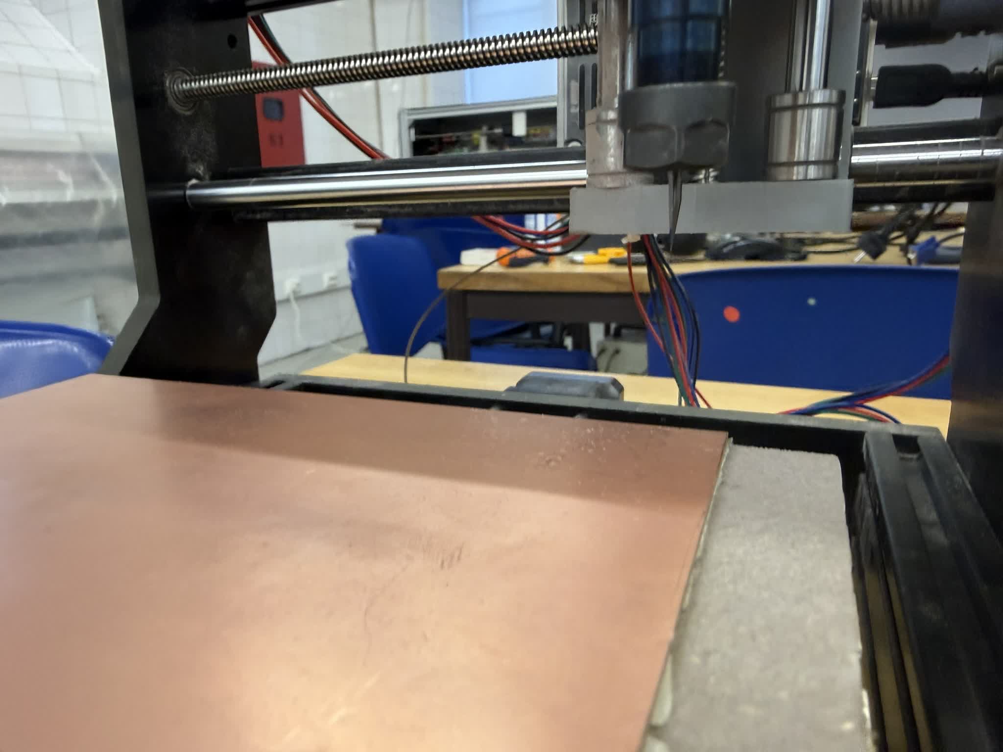
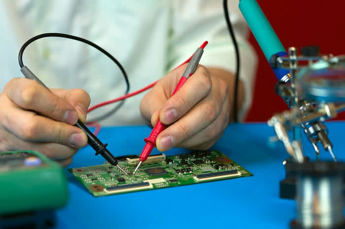
Then, I soldered the wire onto the copper board for electronic leveling. An important note is that you be VERY PATIENT with it since it is technically heating up the whole board. It might’ve probably been more convenient to solder before sticking the fixturing the copper board.
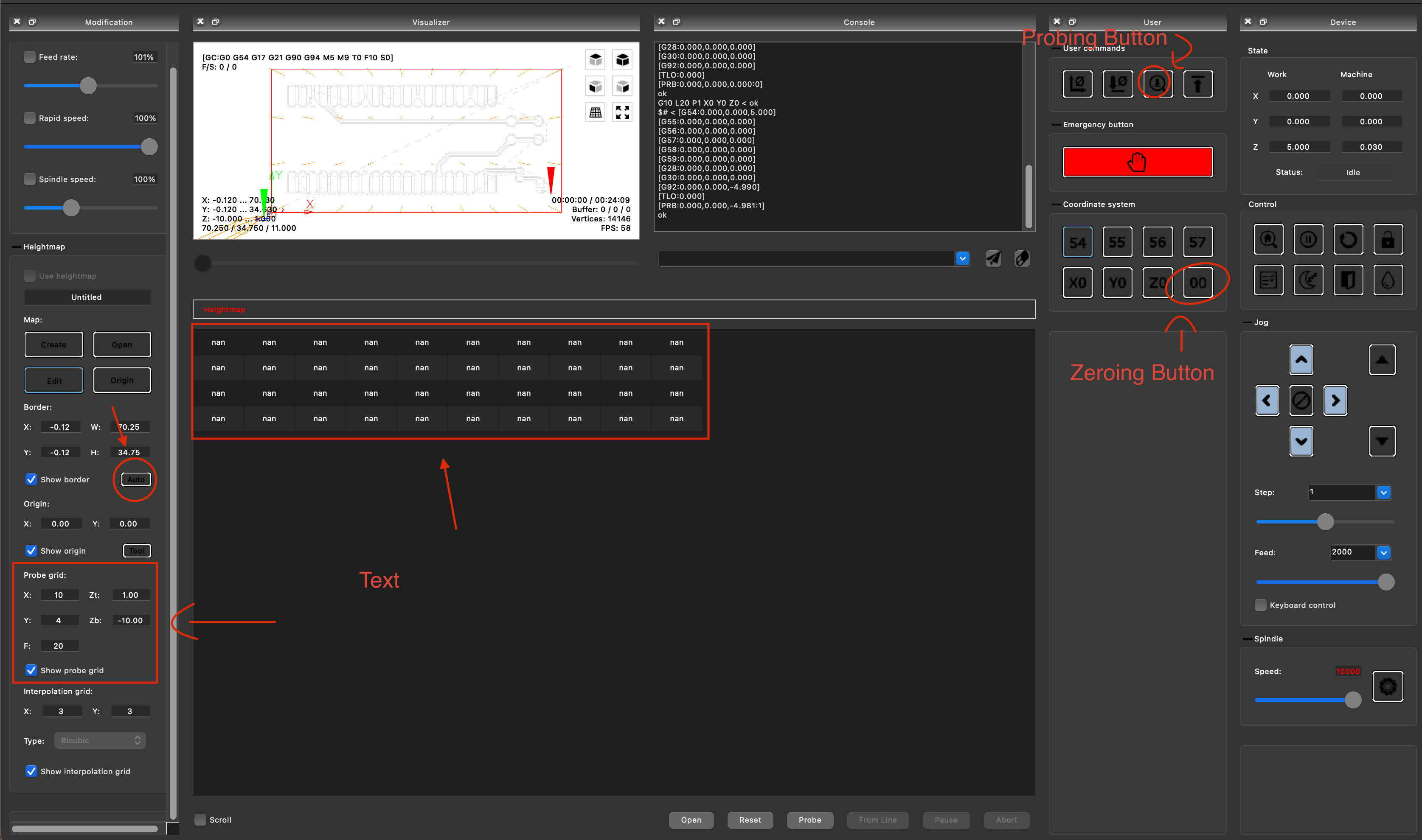
Now, back to Candle were we will set up the zero in all three directions. First step, is to place the spindle on the xy-plane where you want it to be, and zero everything.
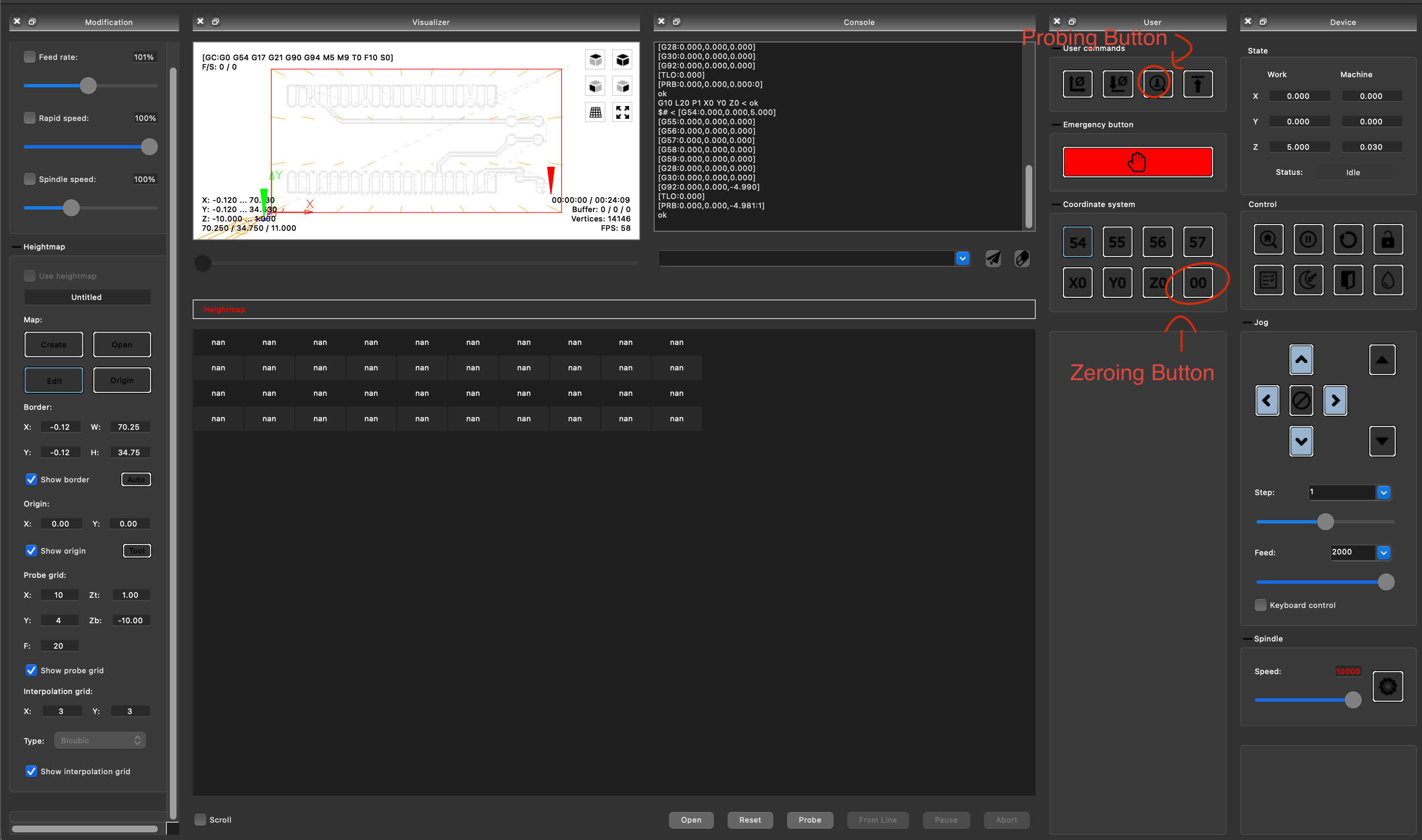
Then, after hooking up another wire to the spindle, you press the probing button to set the zero of your machine in all three directions.
One important note is that you don’t press the zeroing button again since that will change the z position you got from probing leading the spindle to be the safety distance above the board (I figured this out the hard way lol).
Here’s the flow: attach wire to spindle > move the spindle to wanted xy position > press the zeroing button > press the probe button to find the correct z position.
Due to different reasons, the copper board might have very slight variation in its height throughout, could be due to the tape or bending amongst other things.
The height-mapping feature on Candle enables us to overcome that by probing different points where our cut will happen and editing the g-code to account for those slight variations.
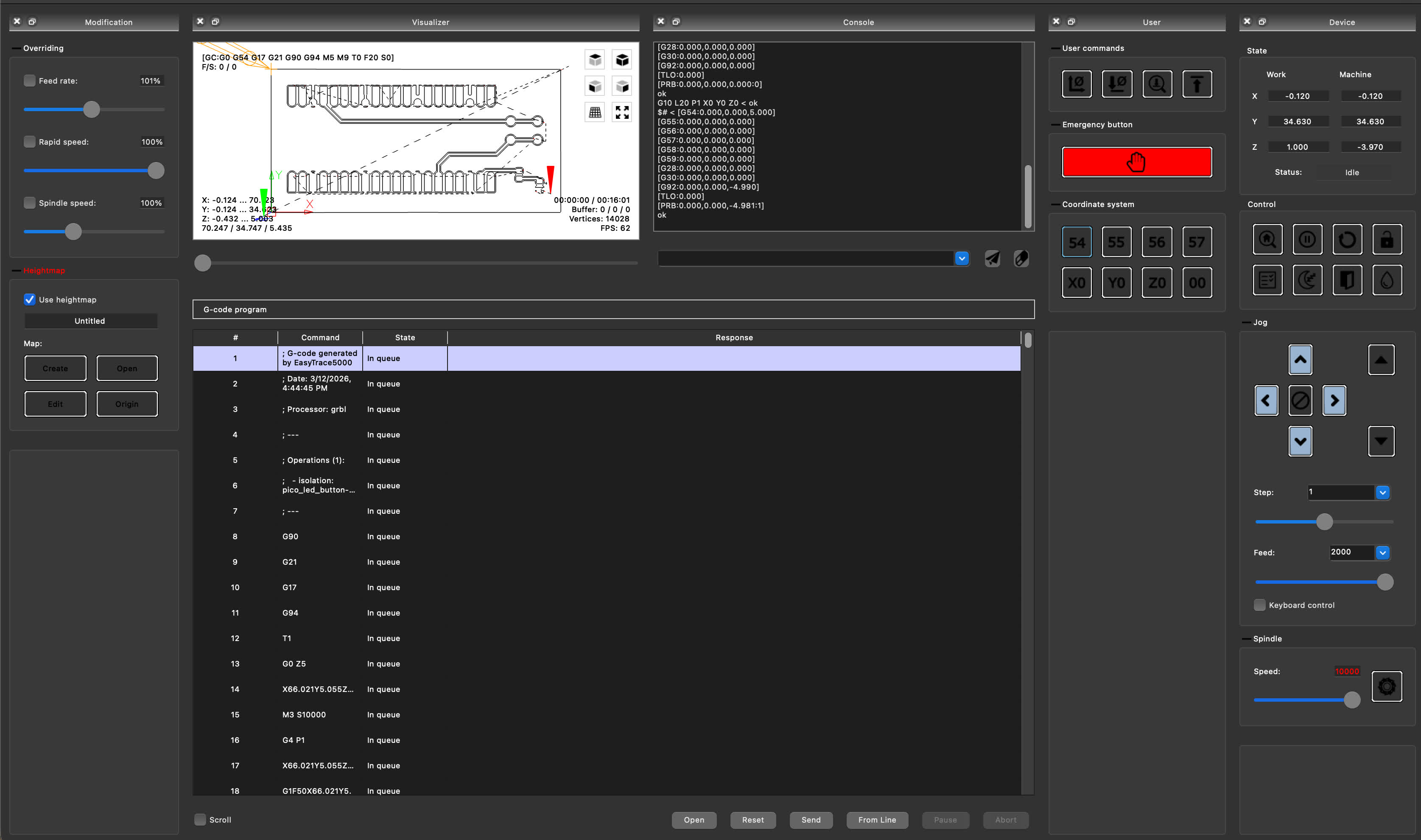
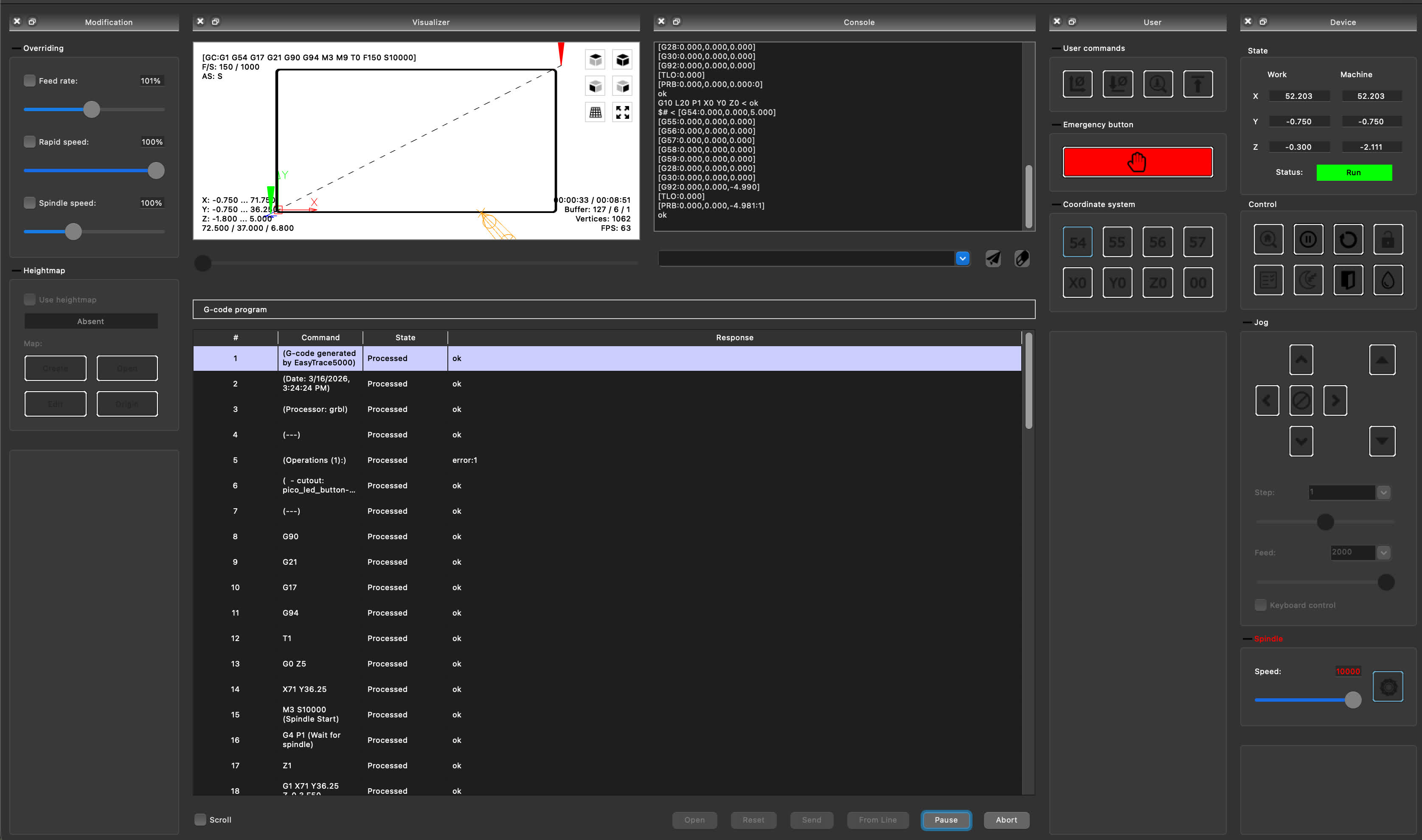
Then, you press send and wait for it finish the cut. You could see the estimated time at the edge of the visualizer and you could override the feed rate at the modifications panel.
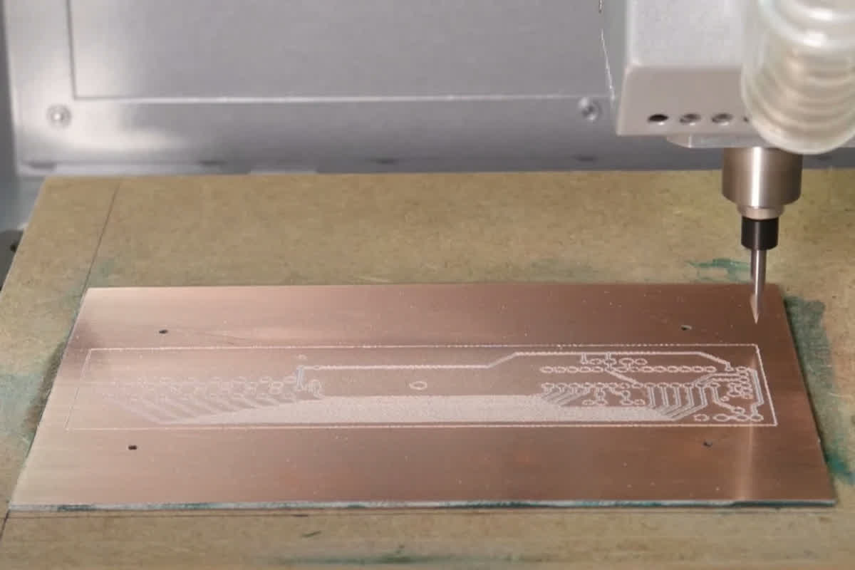
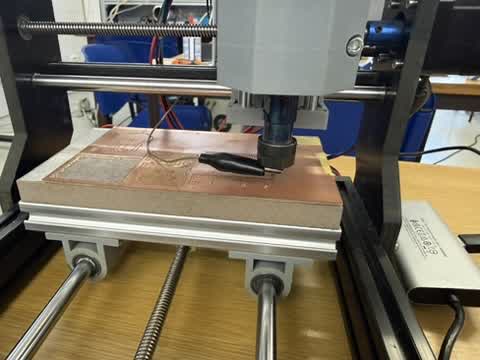
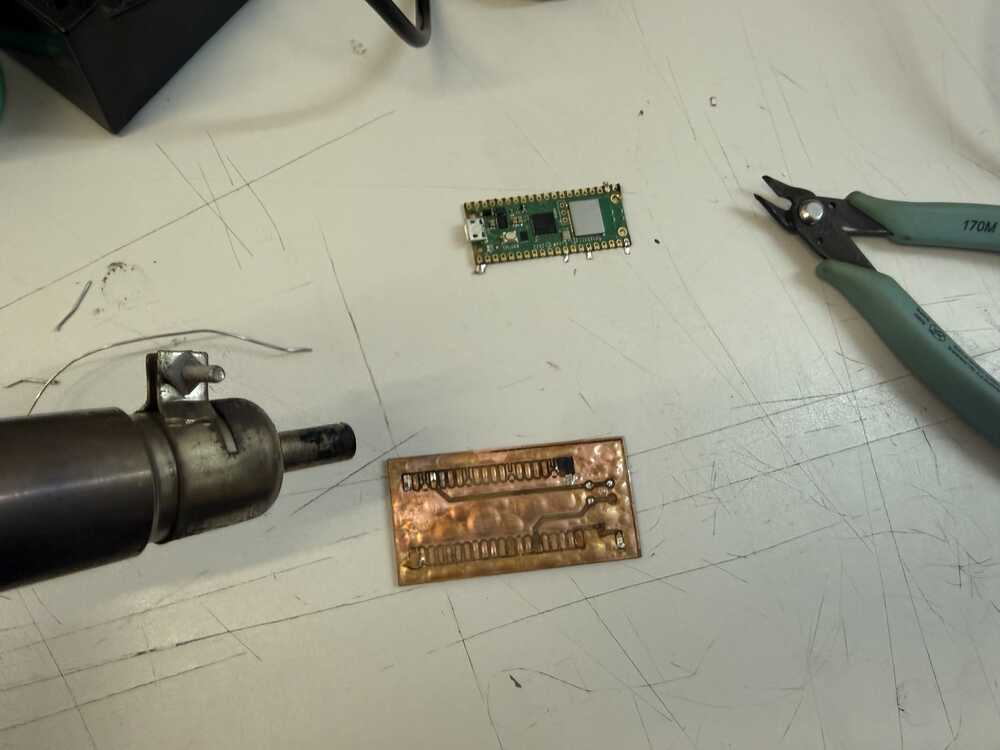
Then, I started cut, and it went smoothly, the depth was all good! Then, I needed to cut the board cutout, so I just changed the mill to a 1 mm flat-end mill.
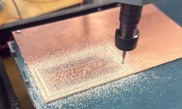
Here’ how the board looked like. I was trying to create a ground pour, but while the vbit was cutting it had a ton of pressure on it so it broke, but it still is a ground pour.
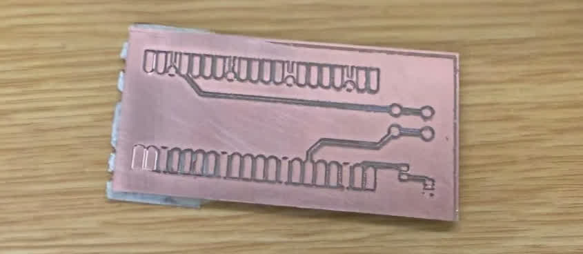
Looking at this photo later, the top-left pad and two lower-left pads were suspicious areas (shoutout to Henk), so I want to note that I cleared the top-left pad after milling. The two lower-left pads were not pins I used for this board, so they did not affect the circuit.
The issue was probably from the copper not sitting perfectly level because of the tape. The board still worked as expected afterwards.
Now, it is time to solder the components on!
Soldering the Components on the PCB
This is my first time every soldering a board. My system was as follows: placed my Raspberry Pi PicoW, and heated up the corner pads using a soldering iron.
Then, I brought the solder to that pin and made contact with the heat gun that adding solder to that pin.
In hindsight, I would use flux to make sure that the solder would only be placed at the pad and not in between the traces.
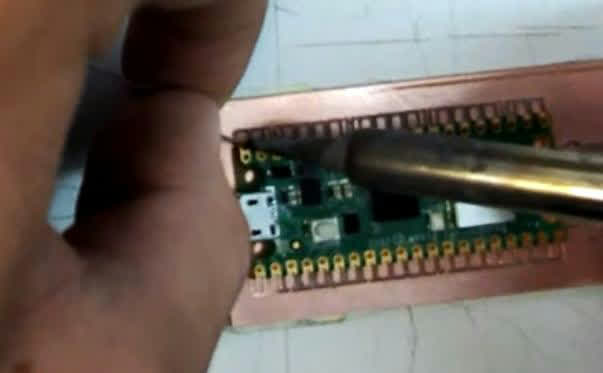
Then, soldering all the smaller components, while soldering, the LED was too small and a bit too difficult for my first time soldering tbh, but it was placed, however, when placing the resistor, I ruined the pads, so successful part of soldering the board was the button and the MCU!
Also, don’t forget that you could just solder the castellated pins you are using, no need to solder everything.
Running My Code
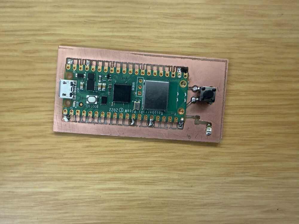
Since the external LED's resistor pads got ruined during soldering, I just used the button I had on the board to control the Pico W's on-board LED instead.
I used PlatformIO with the Arduino framework to program the Pico W. Here's the platformio.ini config:
[env:picow]
platform = https://github.com/maxgerhardt/platform-raspberrypi.git
board = rpipicow
framework = arduino
board_build.core = earlephilhower
upload_protocol = picotool
And here's the code (main.cpp):
#include <Arduino.h>

#define BUTTON_PIN 11

void setup() {
    pinMode(LED_BUILTIN, OUTPUT);
    pinMode(BUTTON_PIN, INPUT_PULLDOWN);
}

void loop() {
    if (digitalRead(BUTTON_PIN) == HIGH) {
        digitalWrite(LED_BUILTIN, HIGH);
    } else {
        digitalWrite(LED_BUILTIN, LOW);
    }
}
The button is connected to GPIO 11 on the Pico W. I set it to INPUT_PULLDOWN so the pin reads LOW by default and goes HIGH when the button is pressed.
LED_BUILTIN is the on-board LED on the Pico W which is routed through the WiFi chip. When you press the button the LED turns on, and when you let go it turns off.
Here is the board functional and operating:
Desoldering Experimentation + Burning the Board
Then, we had a heat plate at the lab, and not lots of instructions about using it. I just got the information that it could be used to desolder, so I thought by heating up the plate up to 350 C, so the solder would melt.
However, that would burn the board immeadiately, and what I learnt later is that I would heat up the board to around 125-150 C and then use a heat gun to melt the solder and the components would come off easily.
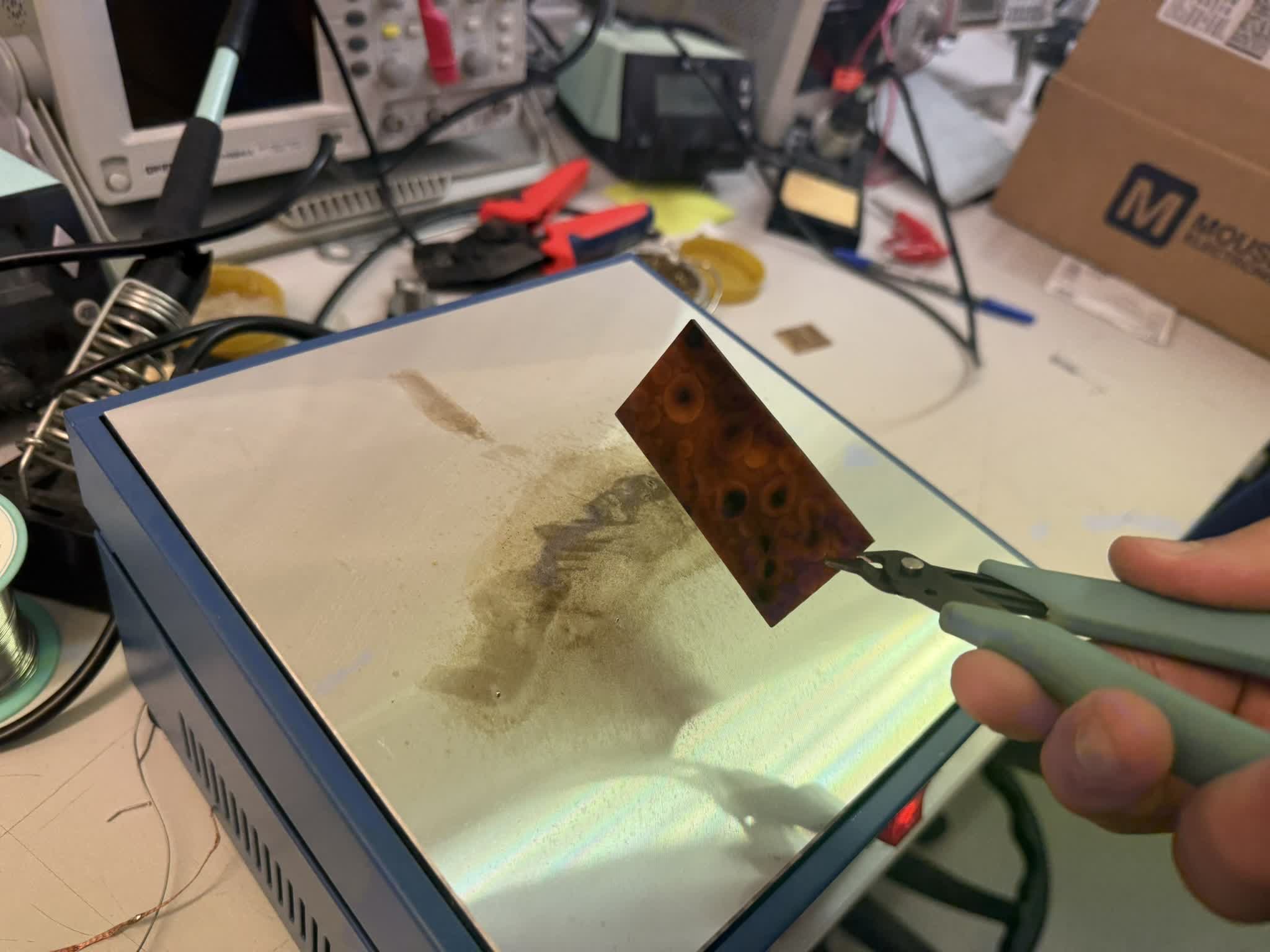
Even though that happened, I still salvaged the MCU!
Original Design and Code Files
- KiCad Design Files
- Code File
- EasyTrace5000 Line Test SVG - the built-in line-test file we used for the milling design-rules test. Created by Eltryus / Ricardo Marques, CC BY-NC 4.0.
This week’s checklist
- Linked to the group assignment page
- Documented how you made the toolpath
- Documented how you made (milled, stuffed, soldered) the board
- Documented that your board is functional
- Explained any problems and how you fixed them
- Uploaded your source code
- Included a ‘hero shot’ of your board