Our lab uses a small desktop CNC mill for PCB fabrication. Unlike the big Ouplan we used in Week 7, this one is specifically for milling circuit boards, removing thin copper from FR1 substrate to isolate traces.
For CAM we used EasyTrace5000, a tool Riccardo created for PCB milling. It takes SVG files and generates G-code with parameters for tool diameter, cut depth, and speed. Post-processor was set to Grbl, and we controlled the machine through Candle.
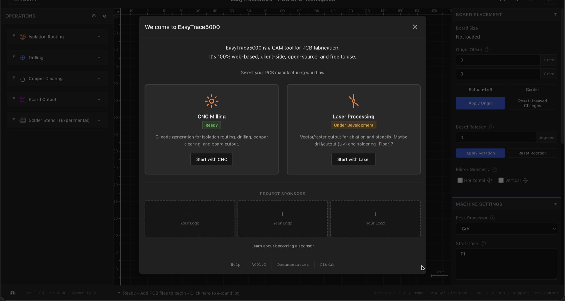
We used a V-bit for isolation routing. Here are the parameters we configured in EasyTrace5000:
| Parameter | Value |
|---|---|
| Tool type | V-bit |
| Starting diameter | 0.249 mm |
| Cut depth | -0.04 mm |
| Copper thickness | 1.8 mm |
| Spindle speed | Not controllable (fixed) |
| Post-processor | Grbl |
| Origin | Bottom-Left |
V-bits let you adjust the effective cutting width by changing depth — go deeper and the cut gets wider. They are noisier and less predictable than straight end mills, but almost impossible to break.
The spindle speed on our machine can't be controlled through software. It just runs at whatever RPM it runs at. Common for these small desktop PCB mills. So the only parameters we could really tune were the tool diameter setting and the cut depth.
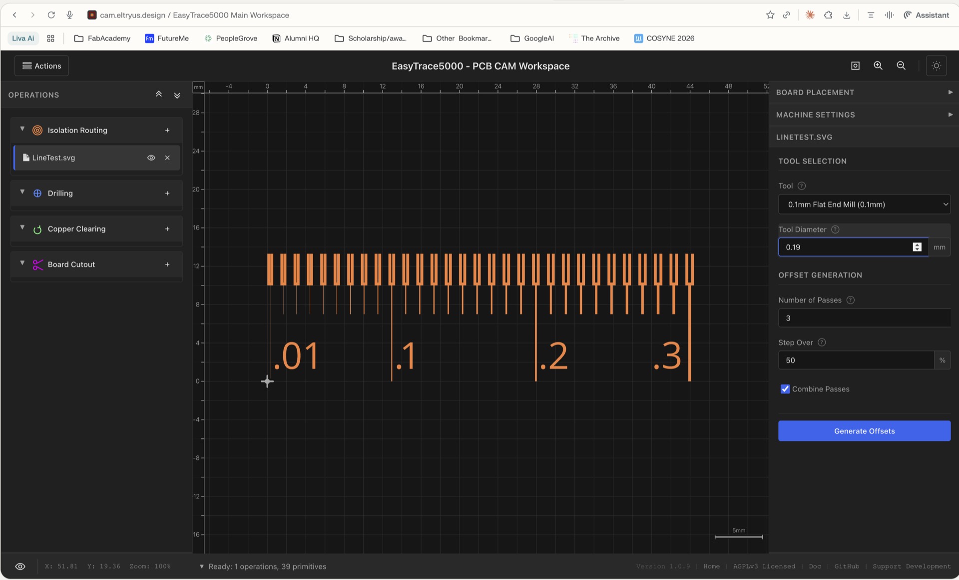
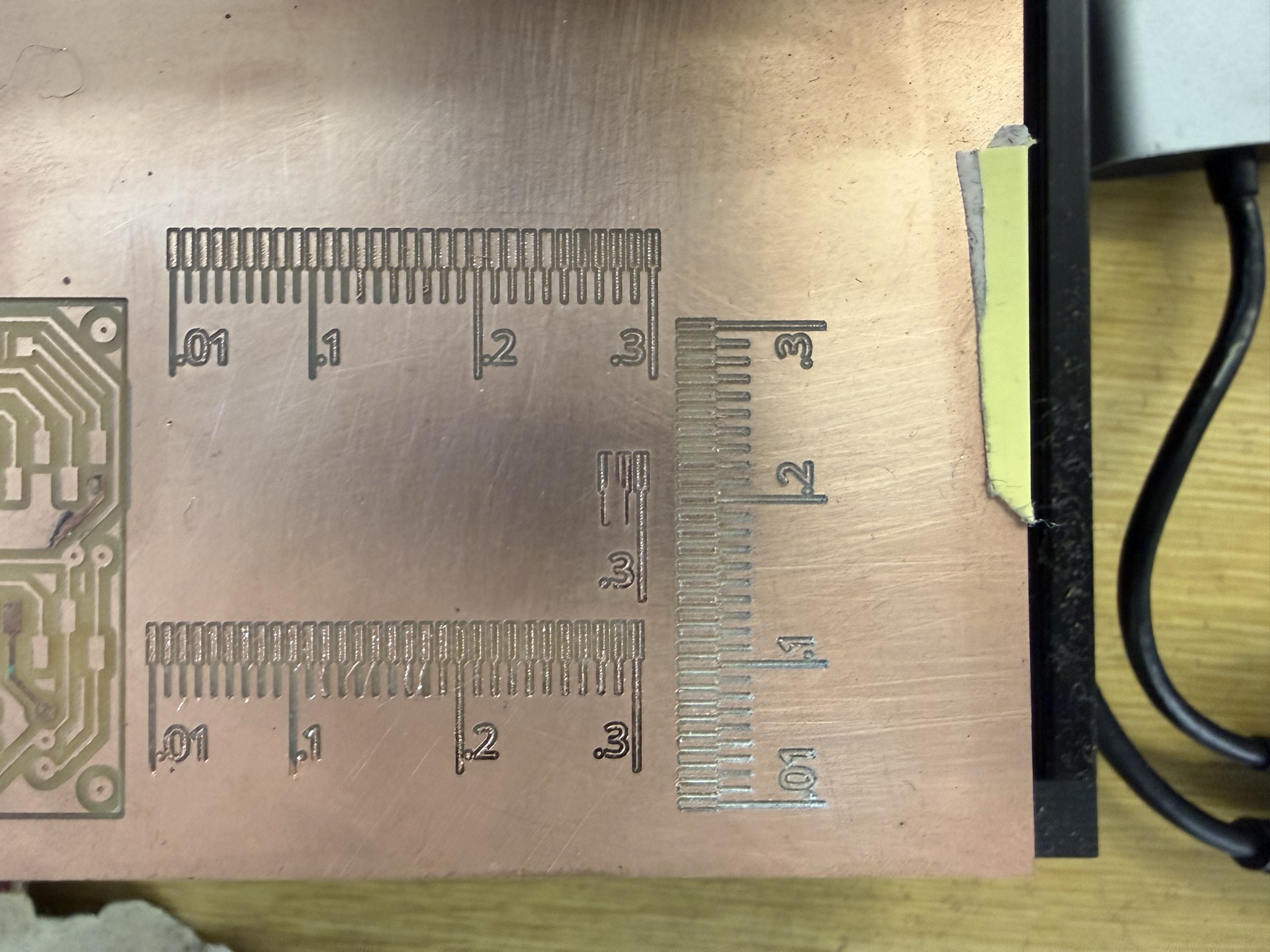
To characterize our machine's limits, we used a line test pattern — an SVG with traces at progressively smaller widths and spacings: 0.3 mm, 0.2 mm, 0.1 mm, and 0.01 mm. Mill it and see what survives.
We secured the FR1 copper board to the machine bed using double-sided tape. The board needs to be perfectly flat because we are cutting features measured in hundredths of a millimeter. Any warping means some traces won't cut through while others get destroyed.
For zeroing Z, we used the probing function on the Candle software where we create a circuit by connecting a wire from the machine to the copper board and the other end of a wire to the v-bit, and probing makes it set the correct Z zero once it completes the circuit.
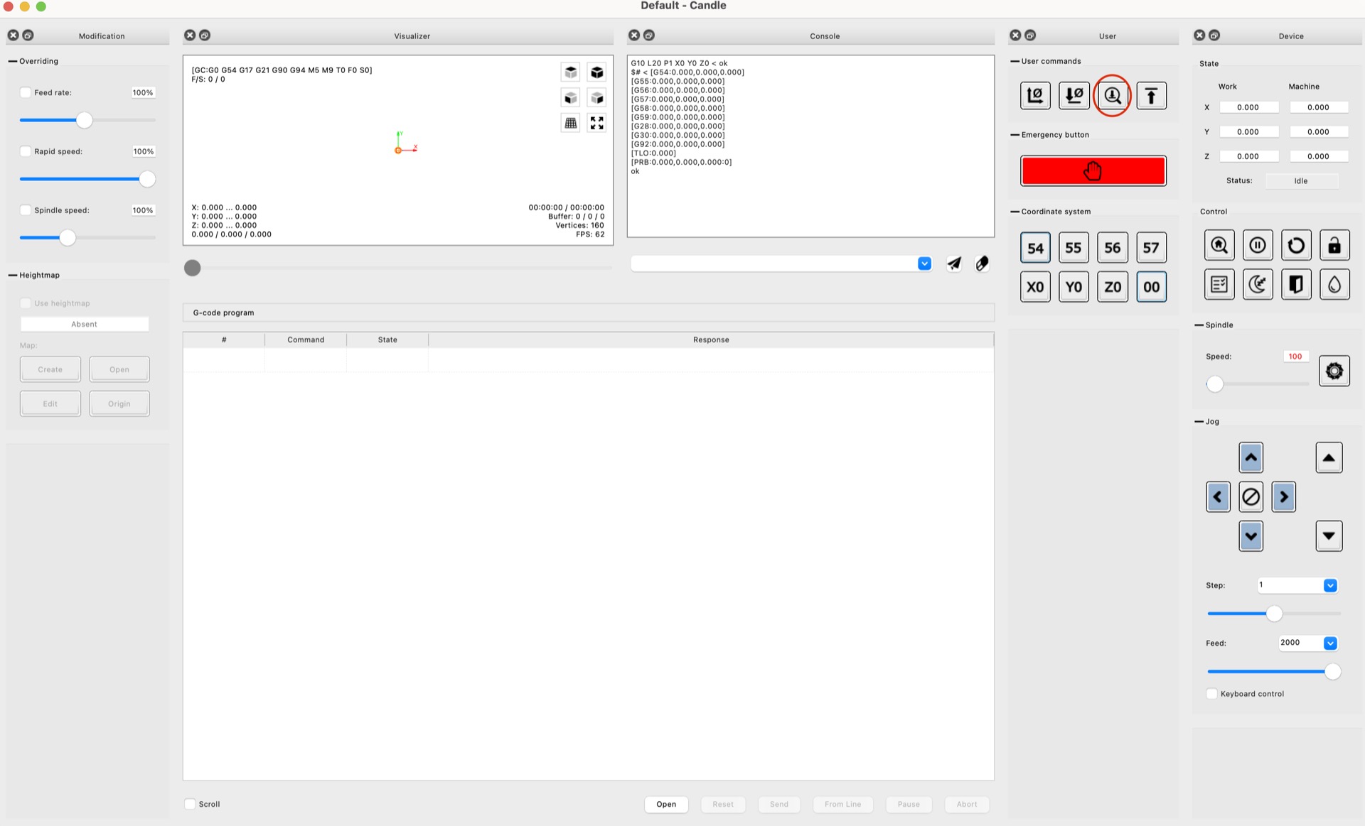
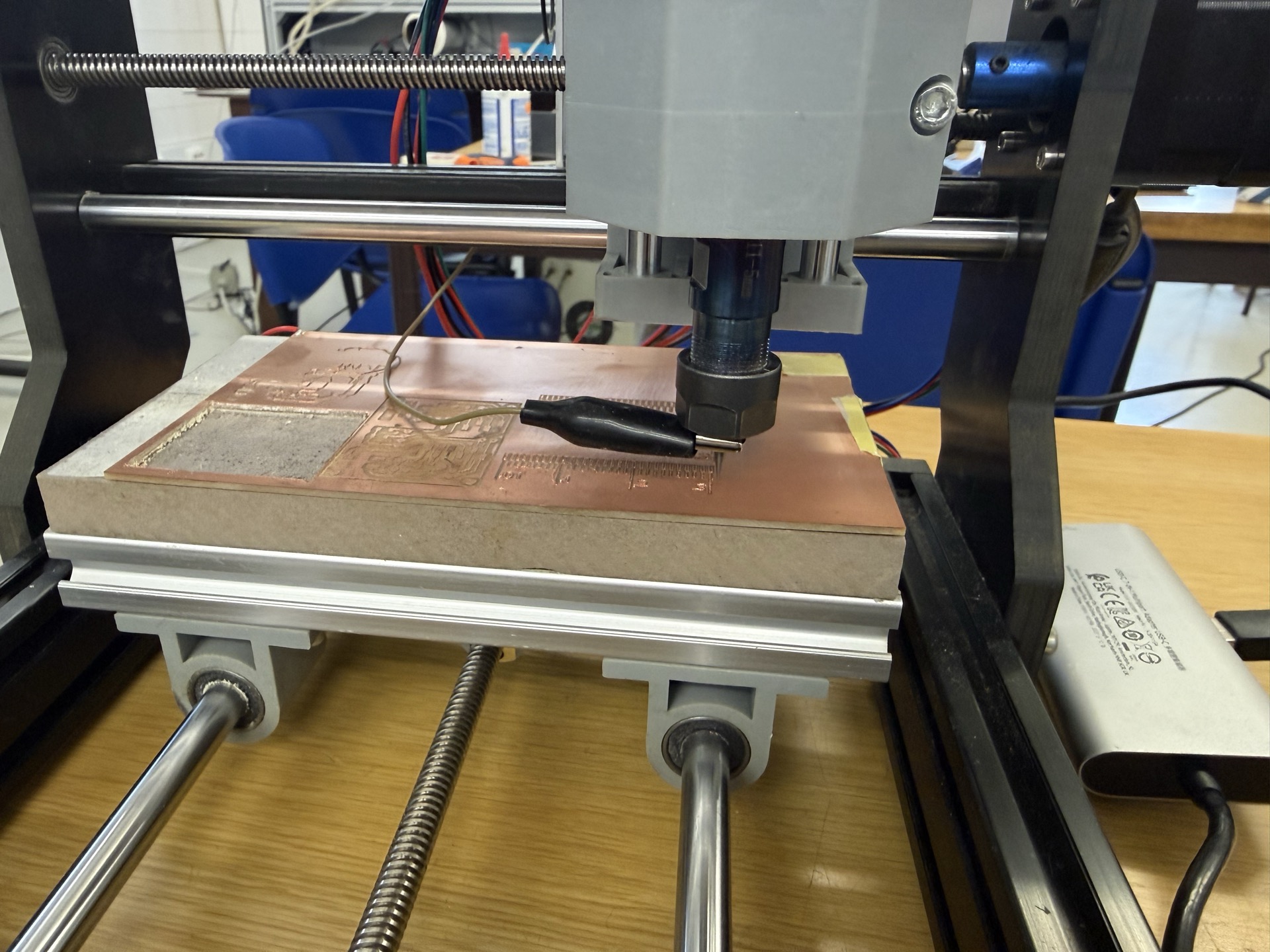
We loaded the G-code from EasyTrace5000 into Candle. It shows a real-time preview of the toolpath and lets you jog the machine, set the origin, and monitor progress.
Additionally, we generated a height map using Candle to account for the hundredth of millimeters of height difference at the surface of the copper.
After milling, we inspected which trace widths and spacings came out cleanly.
| Design Rule | Value |
|---|---|
| Minimum trace width | 0.2 mm |
| Minimum trace spacing | 0.2 mm |
The 0.2 mm traces and spacings came out clean and well-defined. At 0.1 mm things started getting unreliable — traces were inconsistent or merged together. At 0.01 mm nothing survived, which makes sense given our tool diameter of 0.249 mm is already larger than that spacing.
So for any board we fabricate in-house, KiCad design rules need to enforce a minimum width and clearance of 0.2 mm. Anything finer goes to a board house.
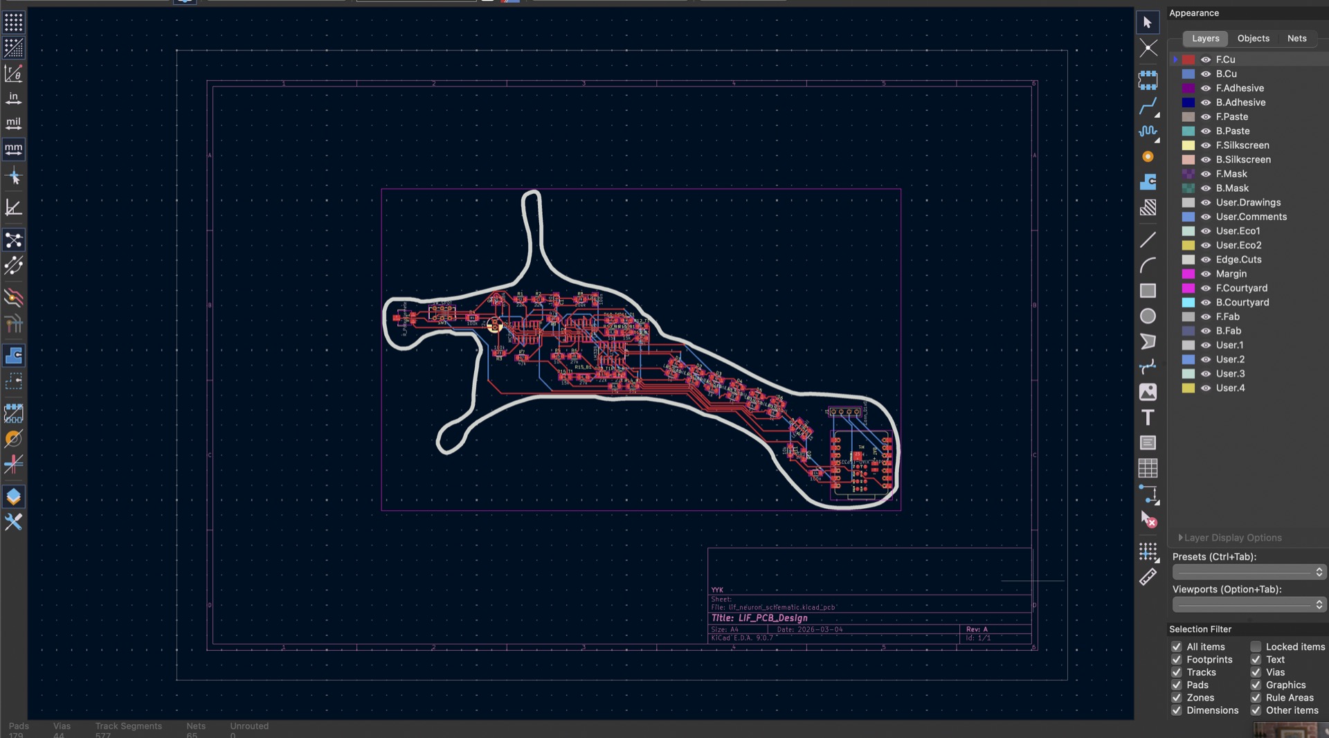
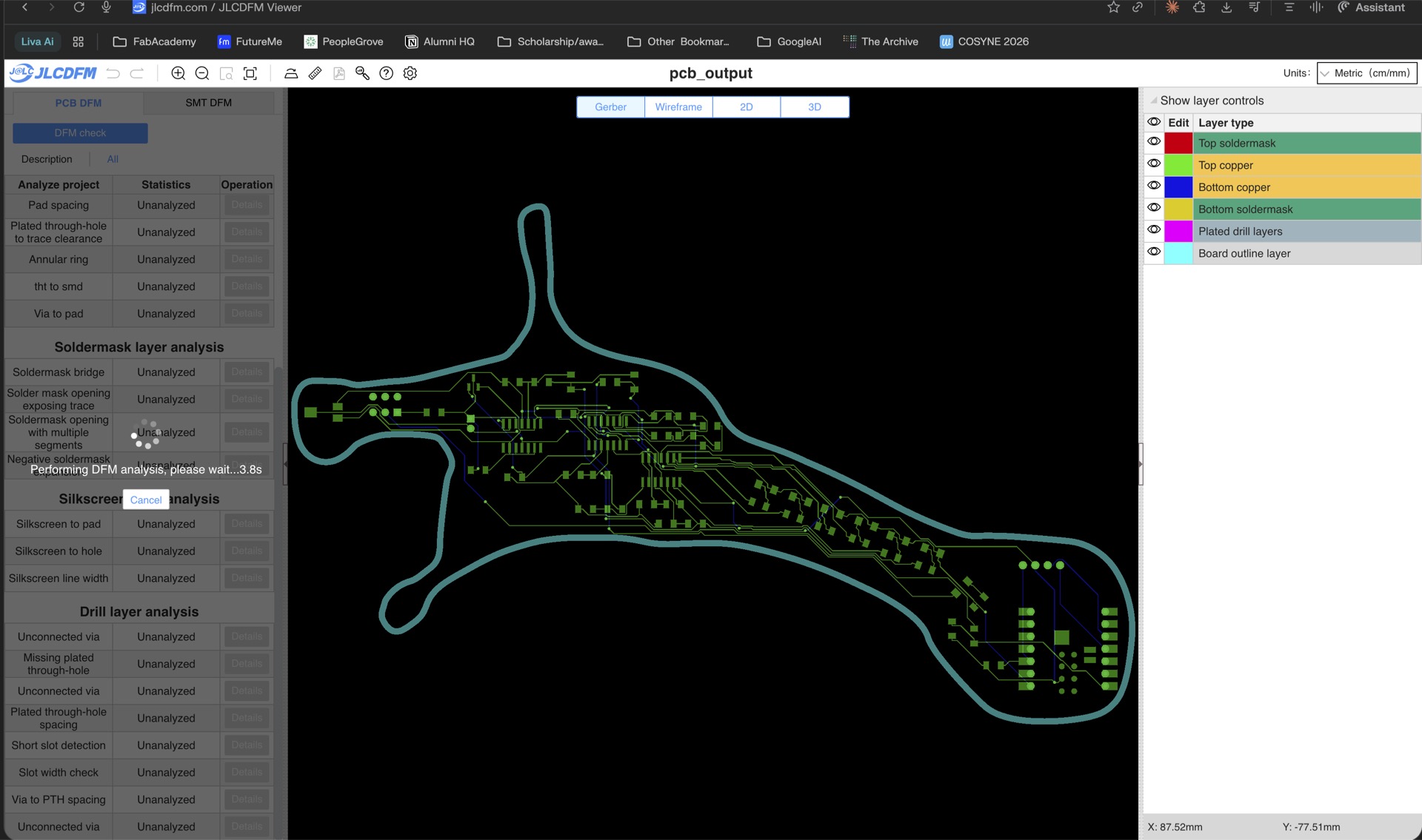
In addition to it being part of our group assignment, the board Youssef designed in Week 6 (the neuron board) was too complex to fabricate in-house. Trace widths and spacings were below our 0.2 mm limit, and the density of the design meant the risk of errors over a full board was too high.
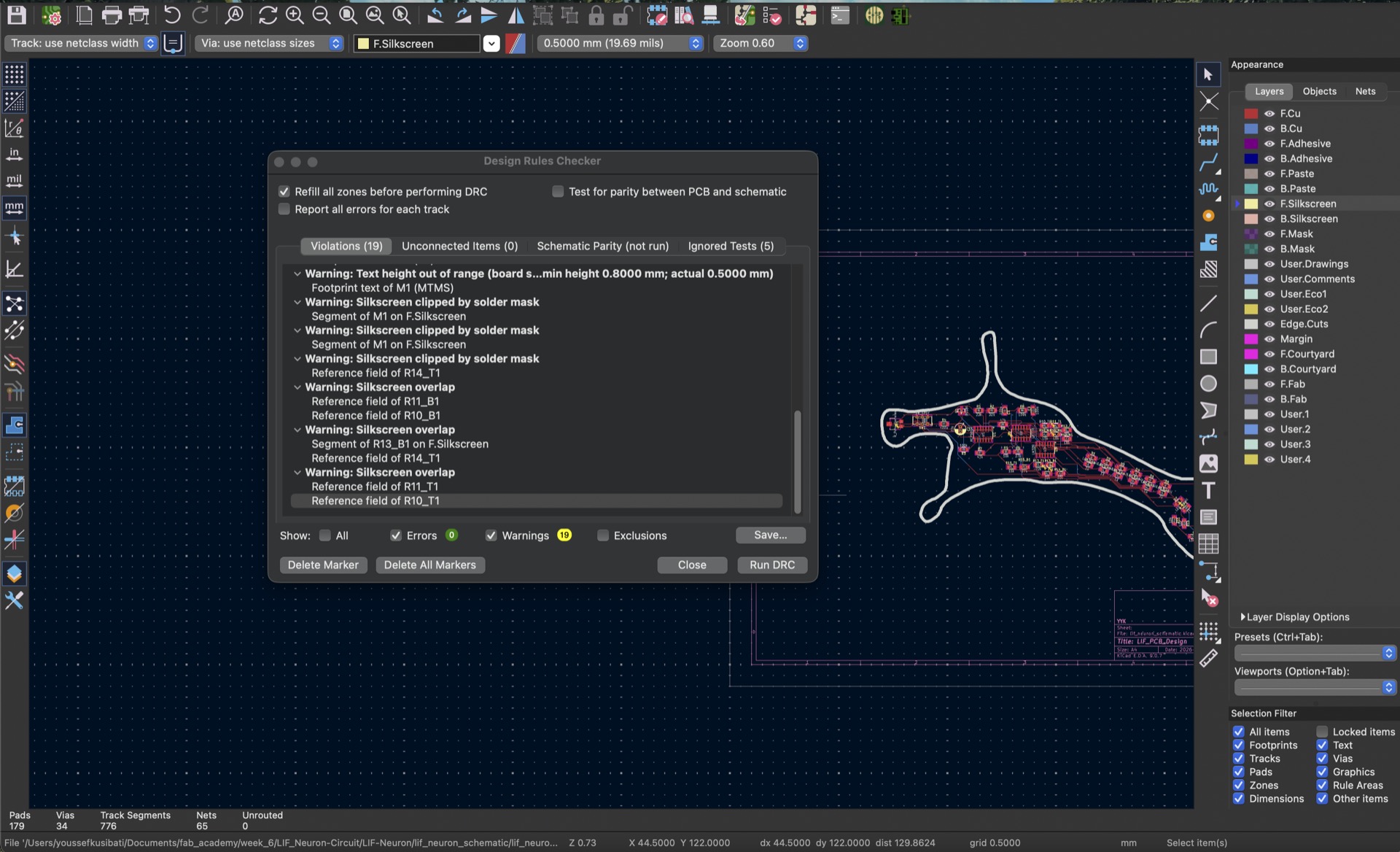
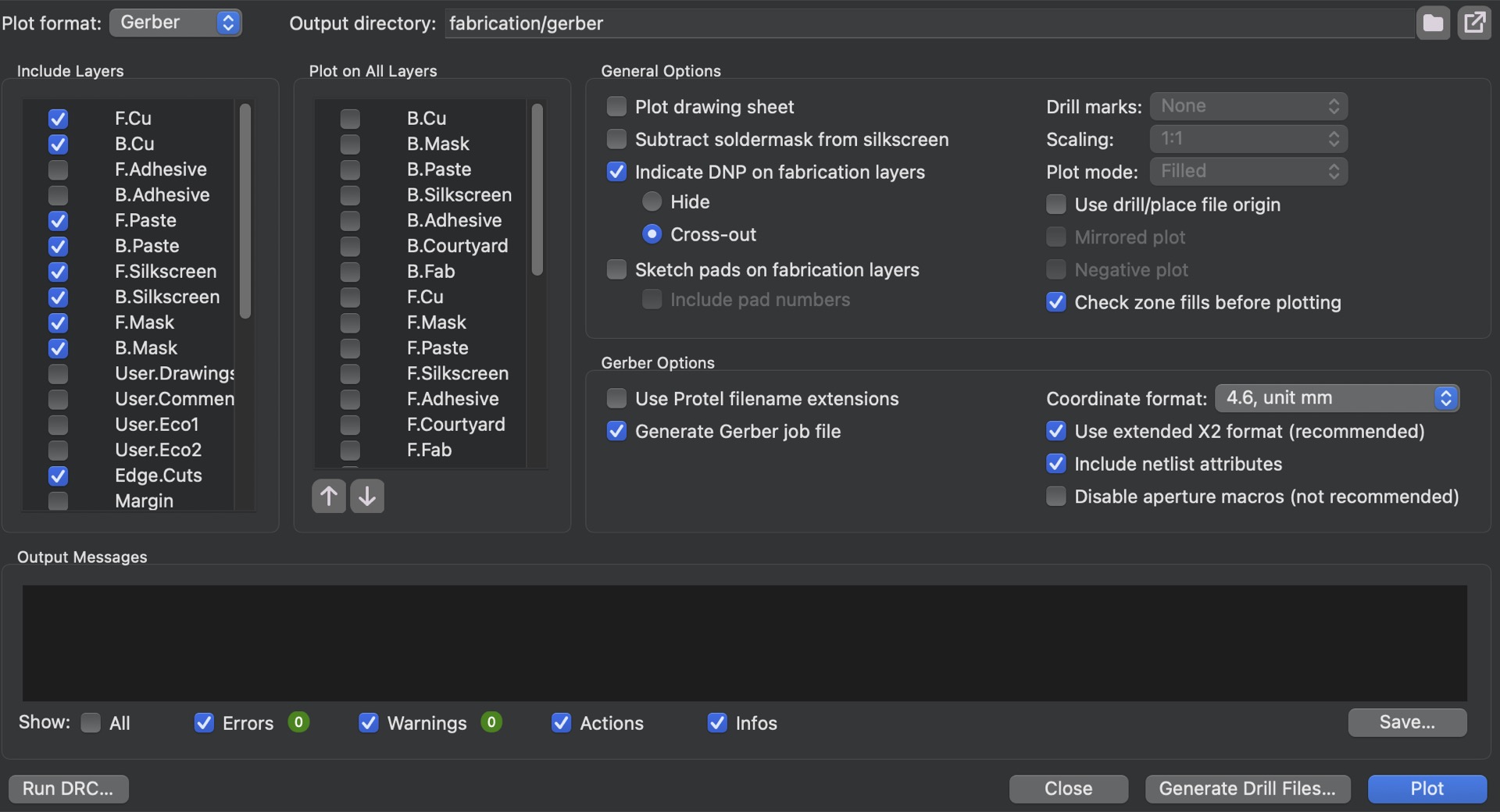
Before submitting, we needed the design to comply with the board house's manufacturing capabilities. They publish their design rules (minimum trace width, spacing, drill sizes, etc.), and your KiCad DRC needs to pass against those.
We edited the design rules in KiCad to match and re-ran the DRC.
To send a board to a board house you export from KiCad:
This is done through File > Fabrication Outputs > Gerbers and File > Fabrication Outputs > Drill Files.
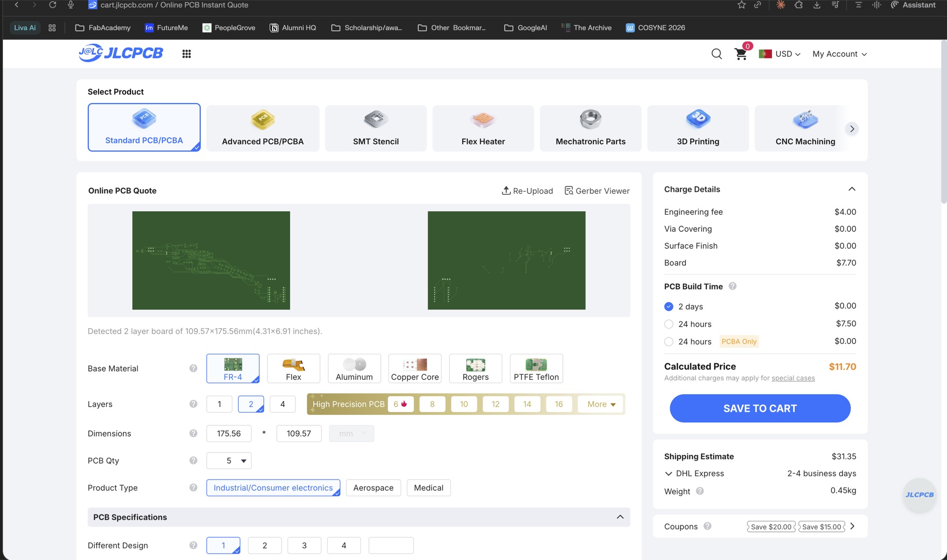
The typical submission workflow, we chose to try out JLCPCB:
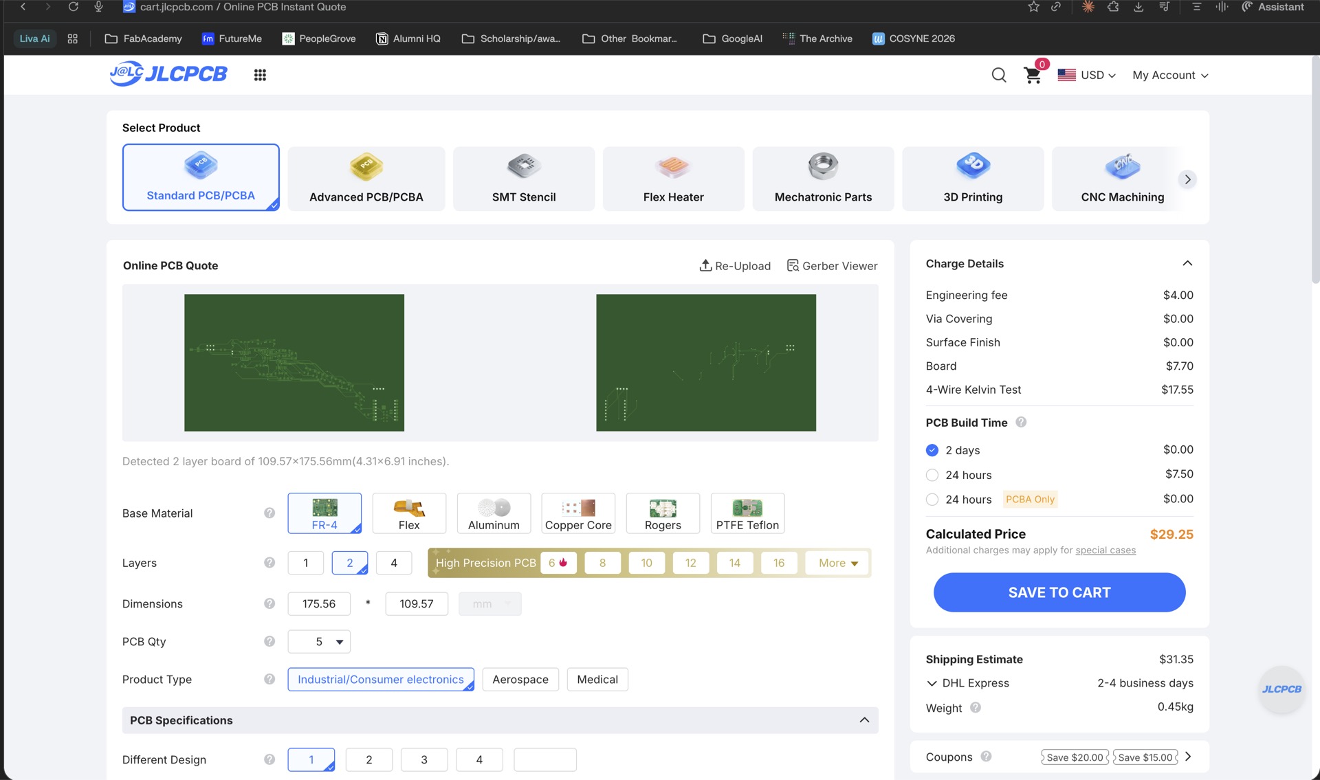
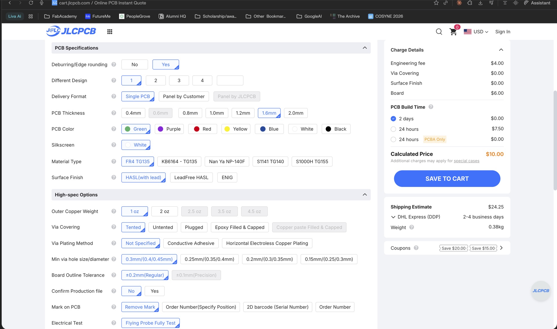
Our in-house mill handles simple single-sided boards with 0.2 mm minimum features. A board house goes down to 0.127 mm (5 mil) or finer, handles multi-layer boards, adds solder masks and silk screens, and plates vias — none of which we can do ourselves.
The trade-off is time and cost. In-house takes minutes and costs nothing beyond the FR1 board. A board house takes days to weeks and costs money. Simple prototypes go in-house, anything with fine-pitch components or dense routing goes out.
