
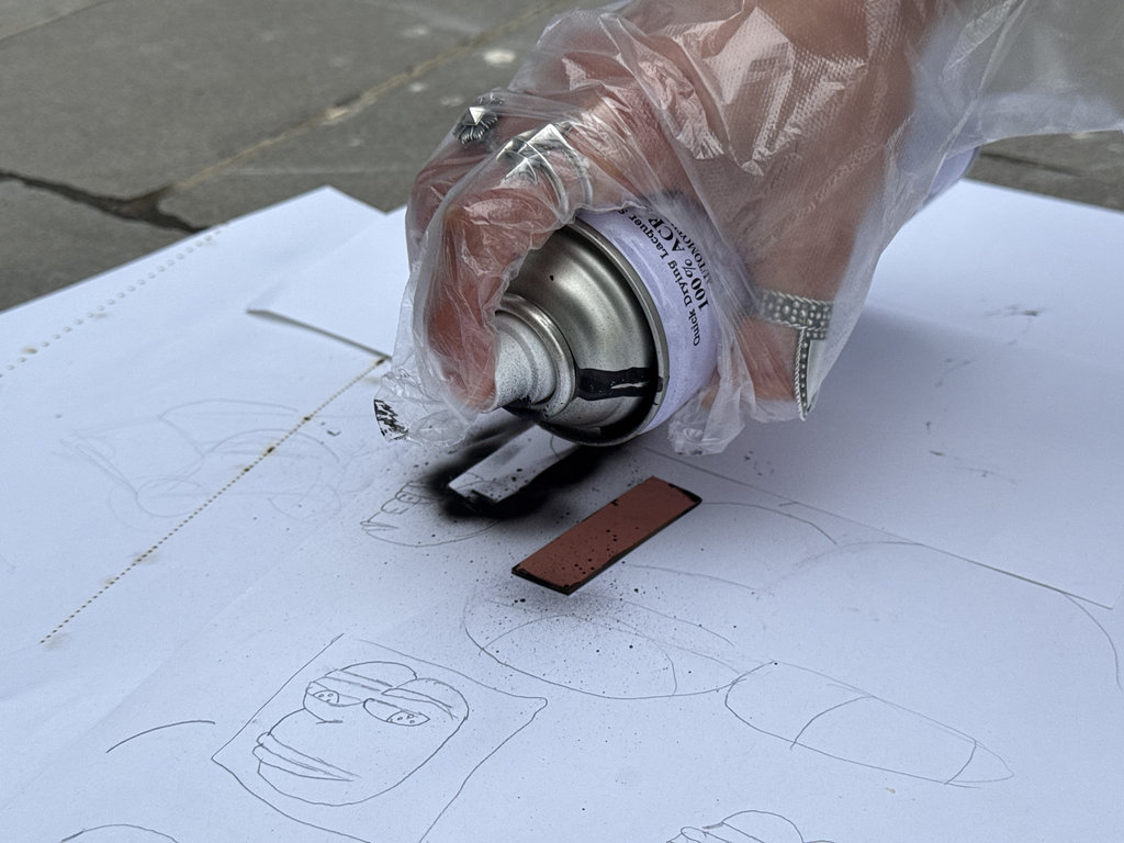
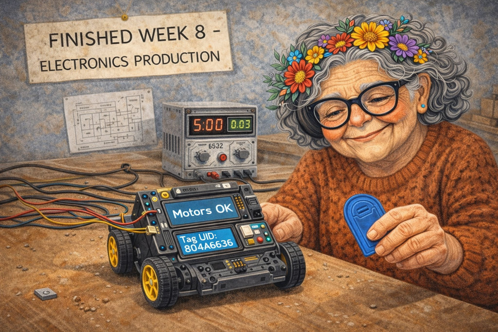
Week 8
AI prompt:
“Can you generate an image about my week 8(Electronics Production)? When this grandmother started cutting her PCB design with the Roland CNC machine, and also tested this PCB and connected to Power supplay and Drive 2 DC Motors, and Also connected NFC Rc522 and want to programm to se tag fine result, and print into I2c LCD Tag id”
Electronics Production
test 1
For the group assignment, we started experimenting with chemical etching to produce a PCB for the required test.
Before starting the chemical etching process, we followed several safety precautions. Even though the chemicals used in this experiment (white vinegar, hydrogen peroxide, and salt) are relatively common household materials, they can still cause skin and eye irritation when mixed together. To ensure a safe working environment, we wore protective gloves and safety glasses throughout the experiment. The chemical solution was prepared and used in a well-ventilated area, and we avoided direct contact with the liquid. After completing the experiment, the remaining solution and materials were handled carefully, and the workspace was cleaned thoroughly.
The etching method is a technique used to remove unwanted copper from a copper-clad board using a chemical solution. In simple terms, it involves protecting the parts of the circuit that we want to keep and then using an etching solution to “bite away” the unwanted copper. As a result, only the conductive traces of the circuit remain.
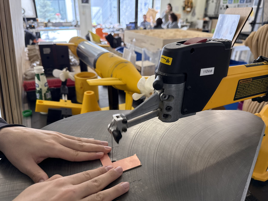
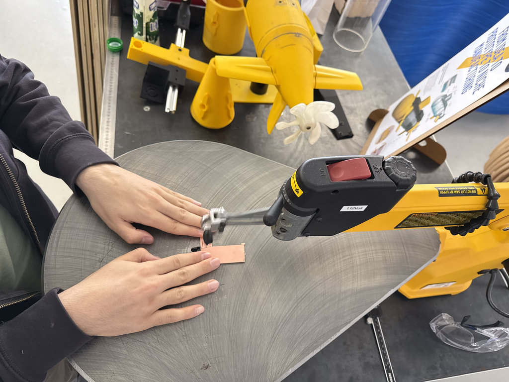
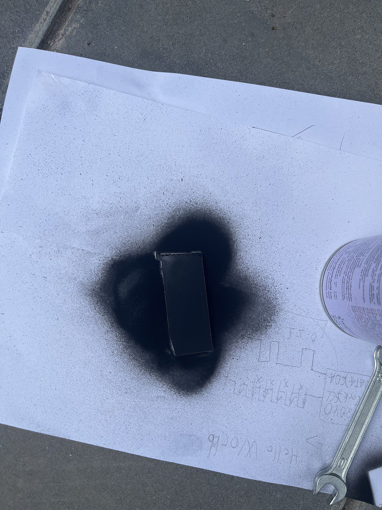
To produce a PCB using chemical etching, we first took a approximately 15 mm × 40 mm copper board and coated it with black paint. Then we prepared the chemical solution in which the board would be placed so that the copper surface could be chemically processed to obtain the desired design.
Here are the required components to prepare the solution.
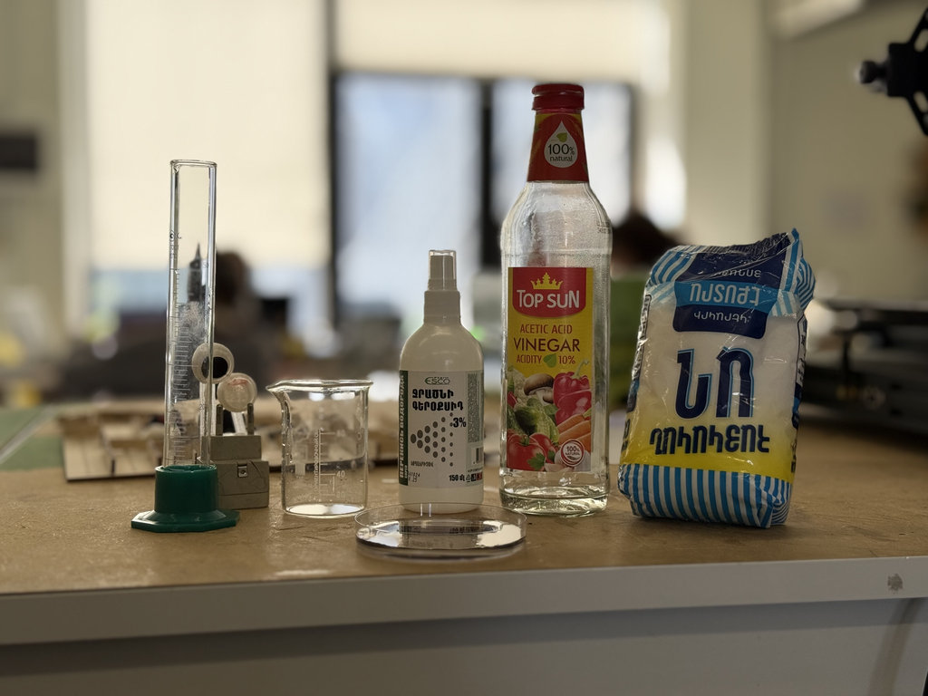
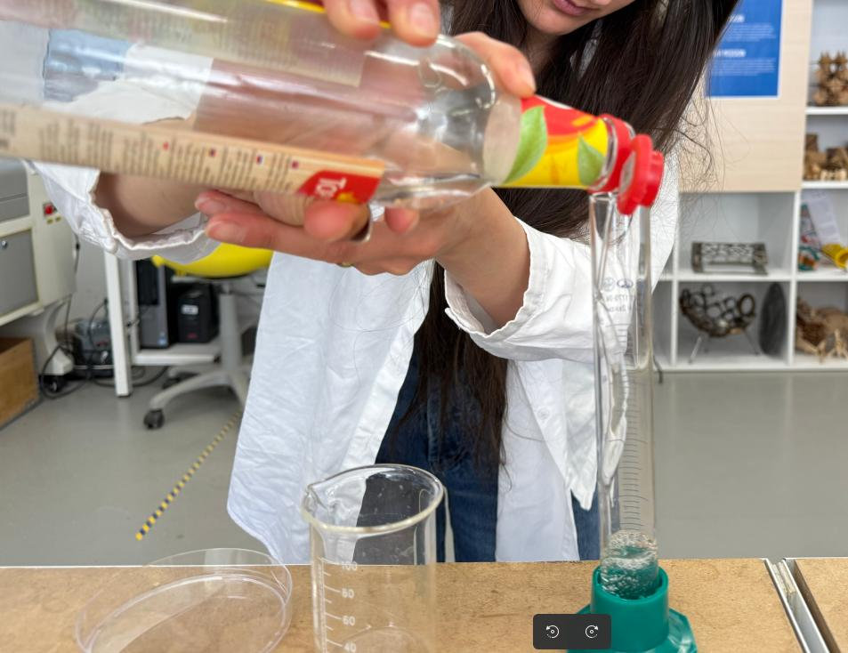
We used 3 parts white vinegar, 2 parts hydrogen peroxide, and a small amount of salt.
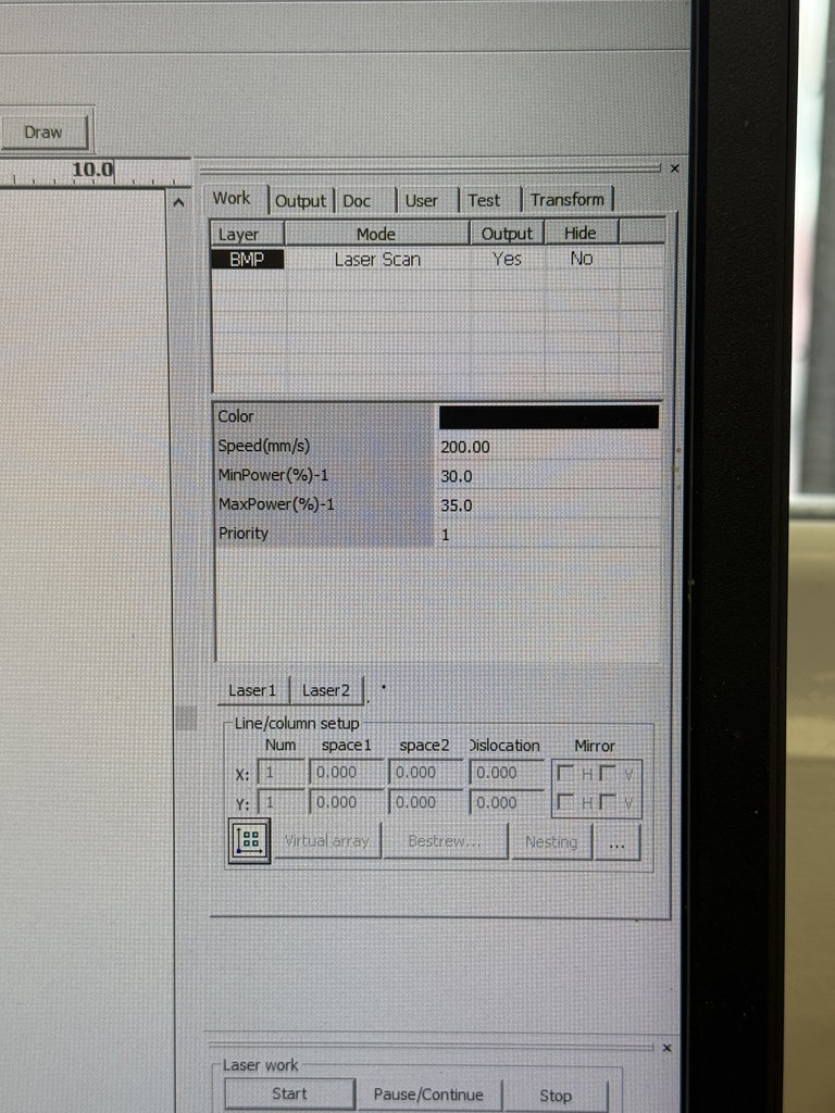
After preparing the solution, we engraved the painted board using a laser cutter to expose the circuit pattern. Below are the laser engraving parameters: speed: 200 mm/min, power: 30%-35%.
And downloaded the test file into this link.
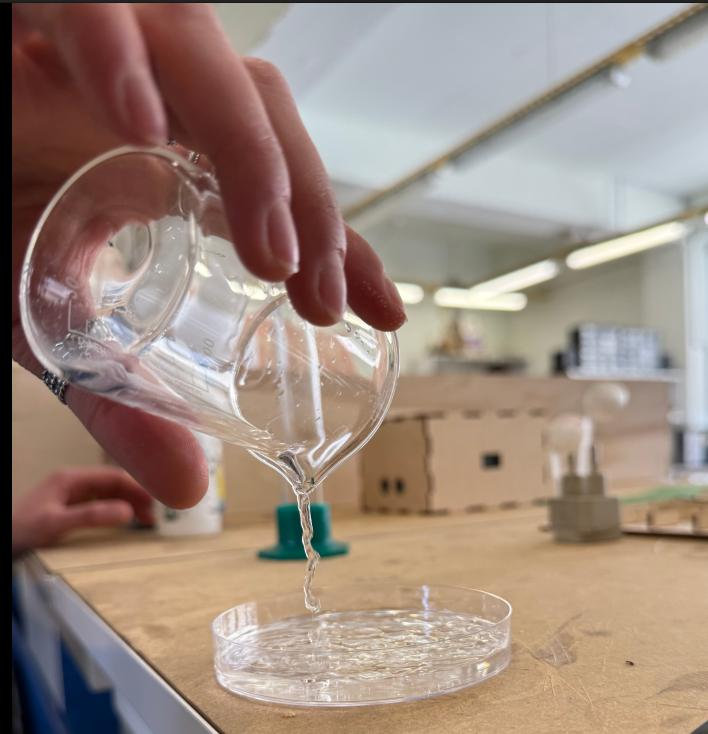
Once the engraving was completed, the board was ready for the chemical etching process.
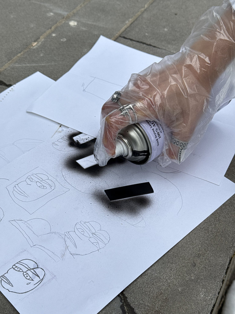
We waited about two hours, but the result was not satisfactory because all the copper areas were removed, not only the unwanted parts.
Here are pictures from the failed process.
test 2
Therefore, we repeated the process again. This time, after painting the board, we left it to dry overnight before continuing with the etching process.
The second version of the chemical etching process also did not work.
This time, we used equal amounts of each component in the solution, hoping it would improve the result.
Unfortunately, the PCB still did not etch properly. At this point, we decided that rather than spending more time experimenting with the chemical process, we would use the CNC milling machine to fabricate the PCB instead. 😄😄😄
You can find the remaining details on the Group Assignments page.
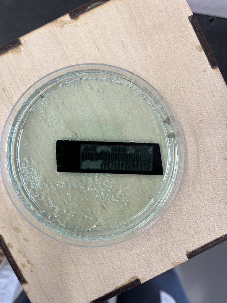
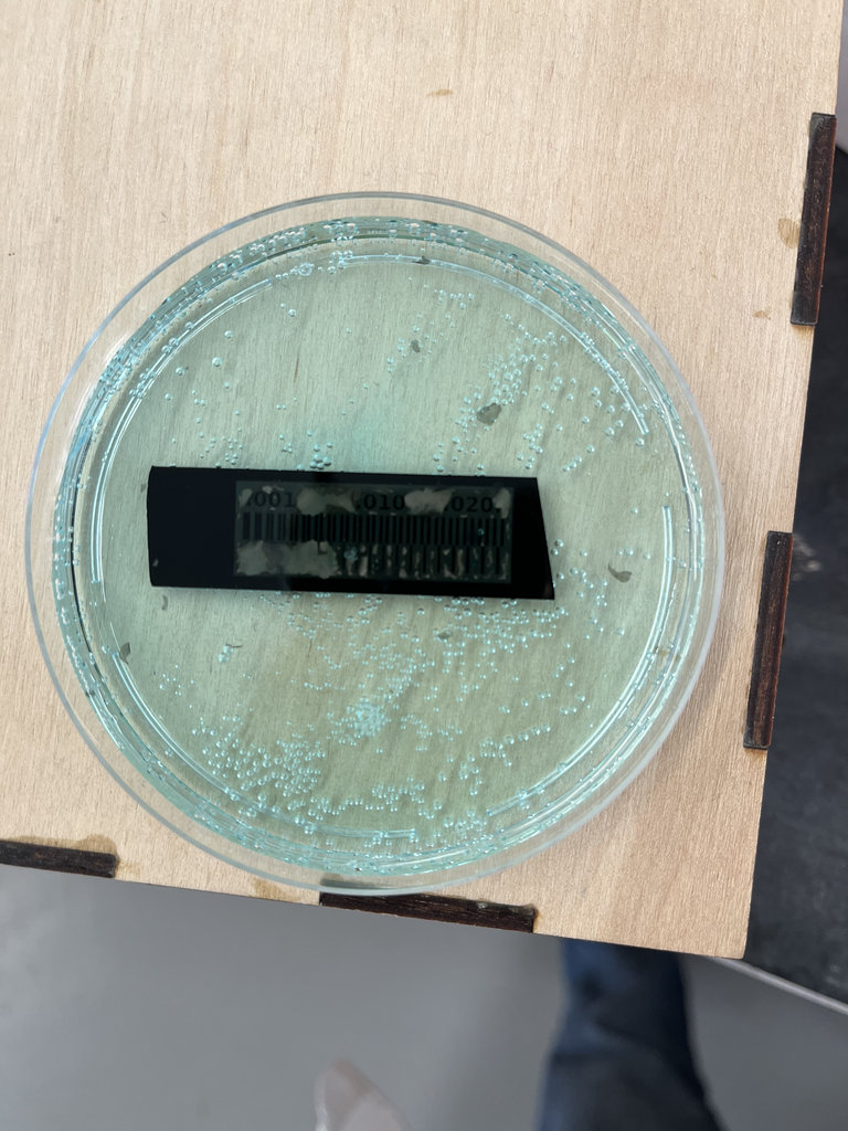
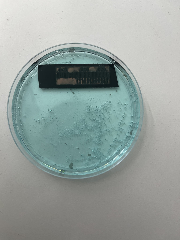
Test 3/4
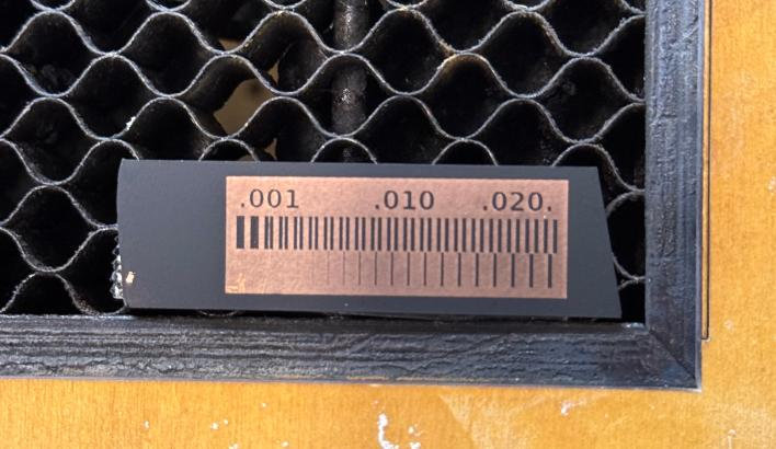
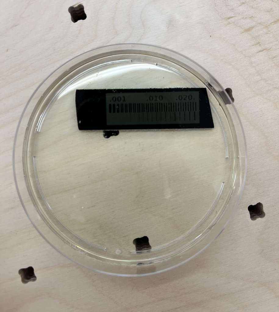
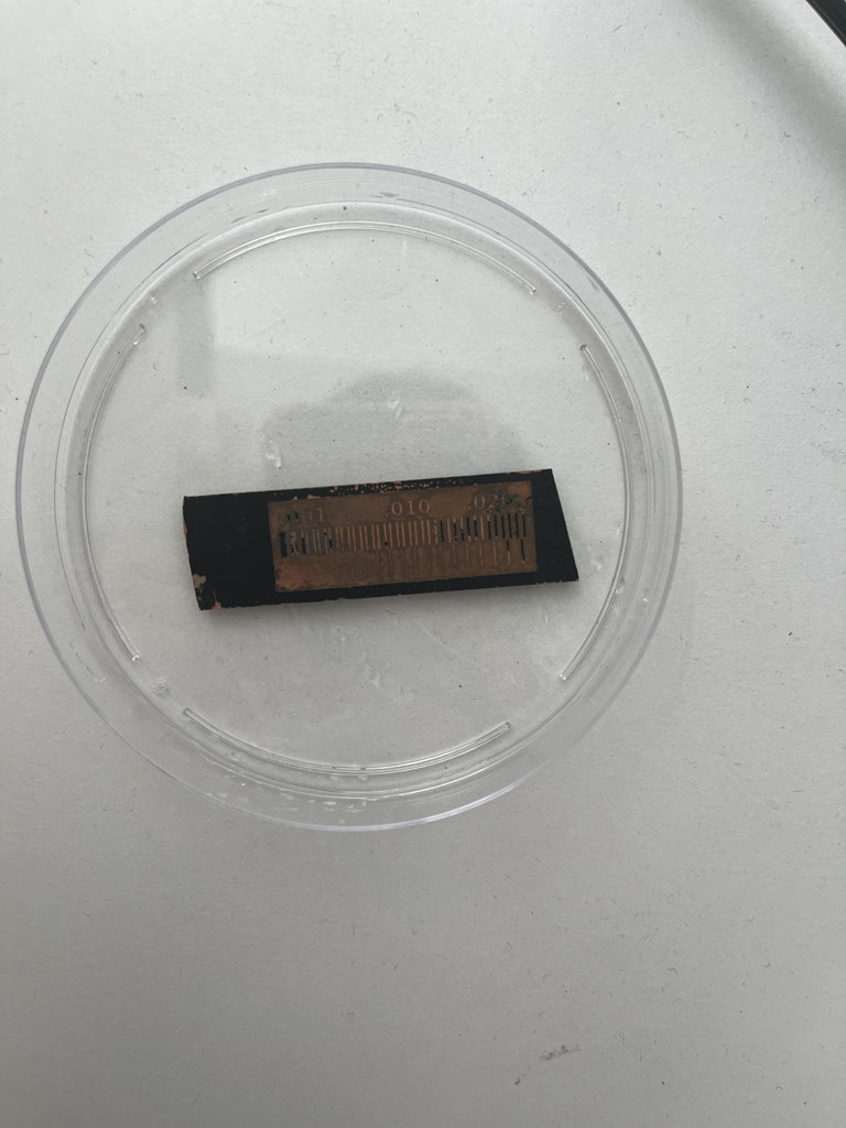
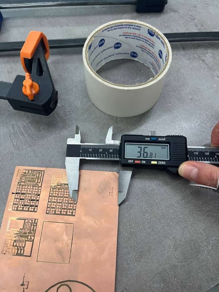
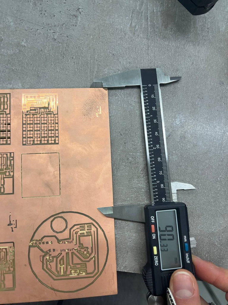
We also performed test engraving using the ROLAND monoFab SRM-20 with this measurement ruler.
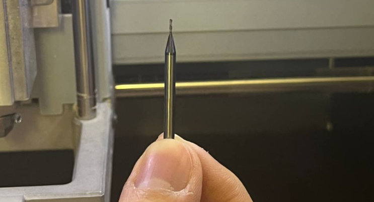
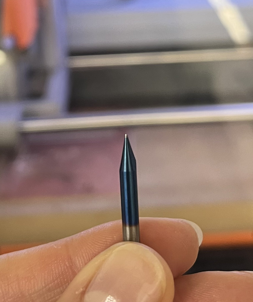
One test was done using a V-shaped 0.1 mm milling bit, and the other using a 1/64 flat end mill.
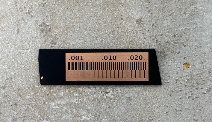
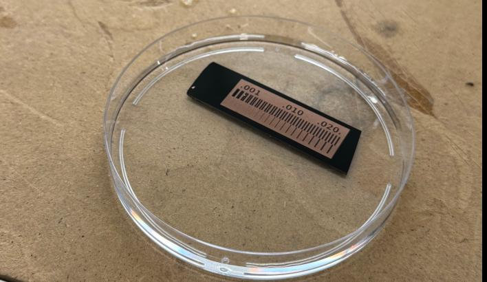
Here are the engraving results.
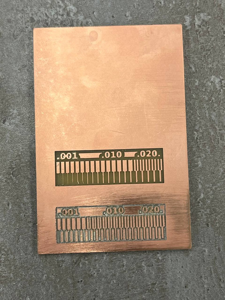
From these tests, we concluded that the 1/64 flat end mill produced more satisfactory results.
Details on the Group Assignments page.
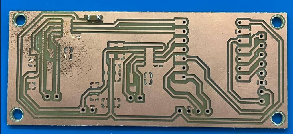
For my individual assignment, I planned to cut the PCB that I designed in Week 6 using a monoFab SRM-20, which is another step toward completing my final project.
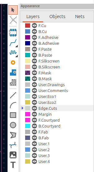
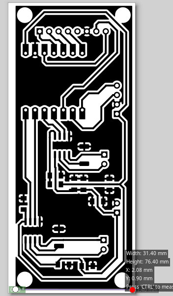
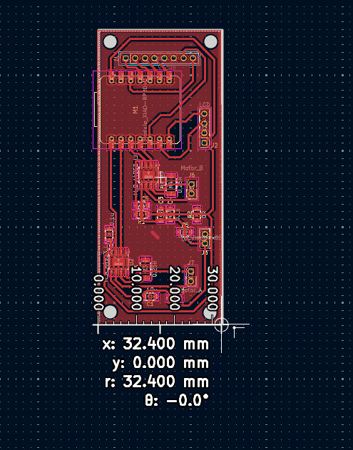
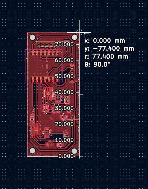
For this purpose, in the design file I added only the Edge.Cuts function, so the monoFab SRM-20 would cut out the PCB shape instead of engraving it. In the Appearance panel, I selected the Edge.Cuts tool and marked the rectangular area that needs to be cut out. I also added circular holes on the edges using the same Edge.Cuts tool so that later I can mount the PCB.
I set the line width of the rectangle to 0.8 mm by double-clicking it, since I planned to cut it with a 0.8 mm milling bit. The radius of the mounting holes was set to 1.6 mm.
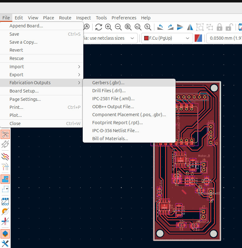
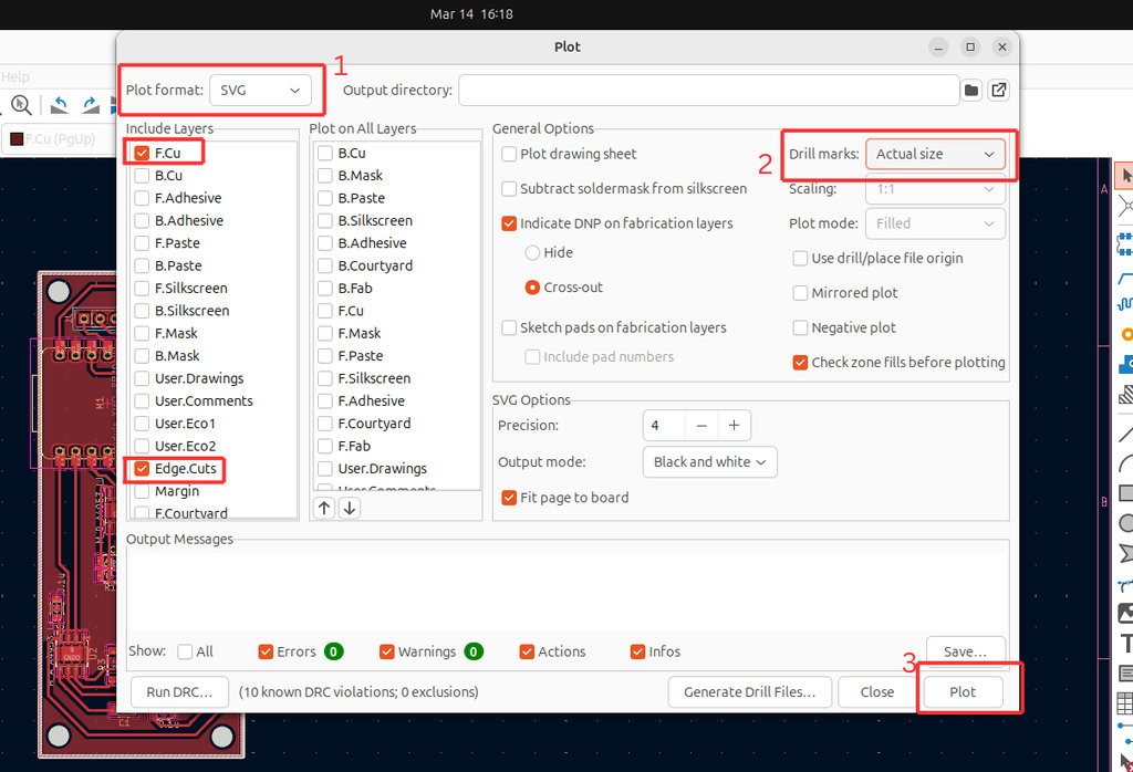
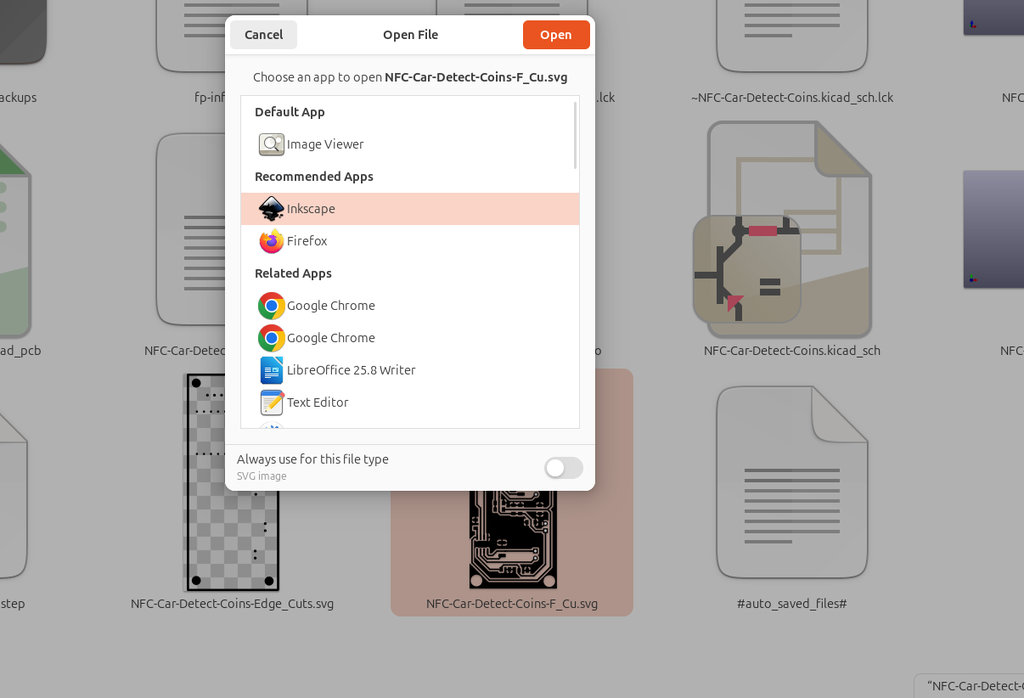
After that, the file was ready to be exported. I selected File → Fabrication Outputs → Gerbers (.gbr). In the opened window, I changed the plot format from Gerber to SVG. I also set Drill Marks to Actual Size. I checked that in Include Layers only F.Cu and Edge.Cuts were selected, since these layers are needed for engraving and cutting. Then I pressed Plot.
Next, I opened the SVG file in Inkscape to verify that the PCB dimensions had not changed.
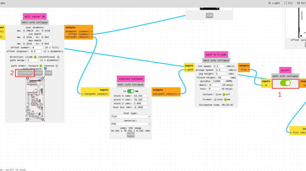
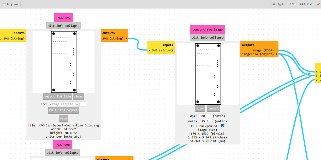
G-code. For this step, I went to modsproject.org and selected Mill 2D PCB from the G-code section.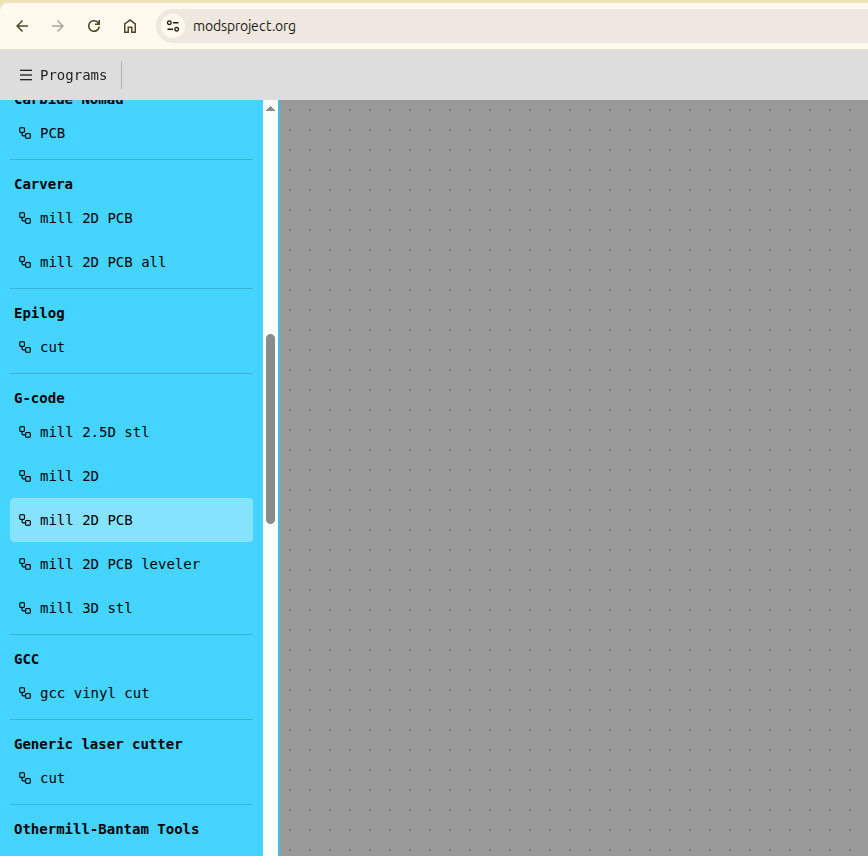
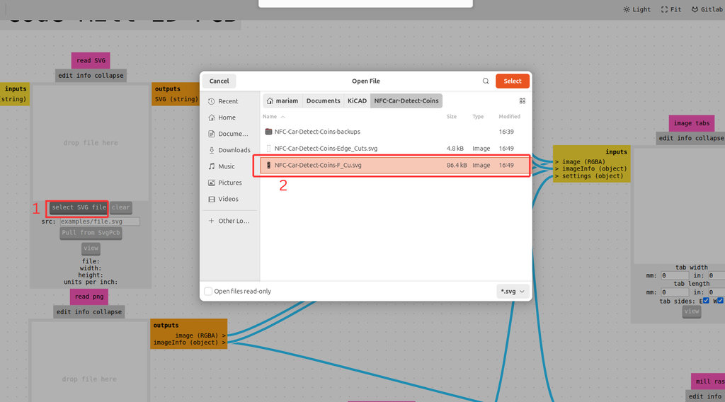
Then I clicked Select SVG file and loaded the saved SVG file.
After loading, the file appeared black with white lines, but it needed to be the opposite because the engraving follows the black traces. Therefore, I performed the invert operation.
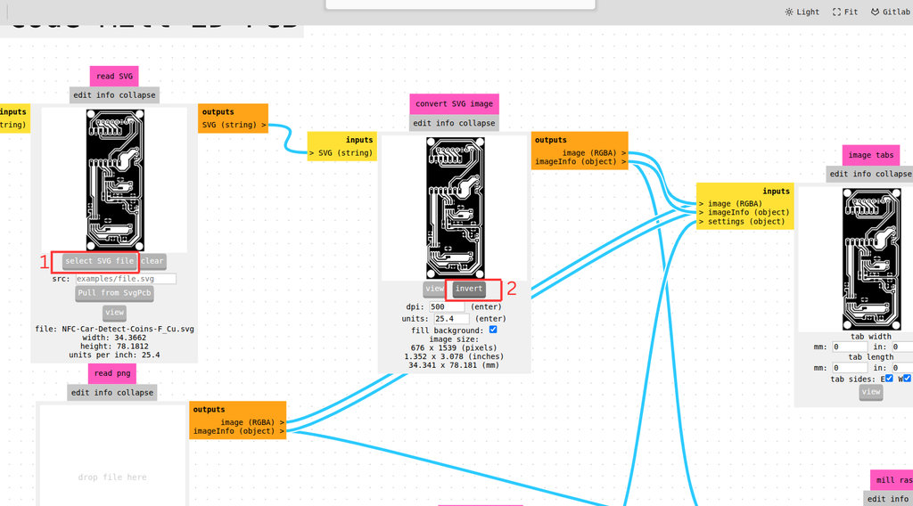
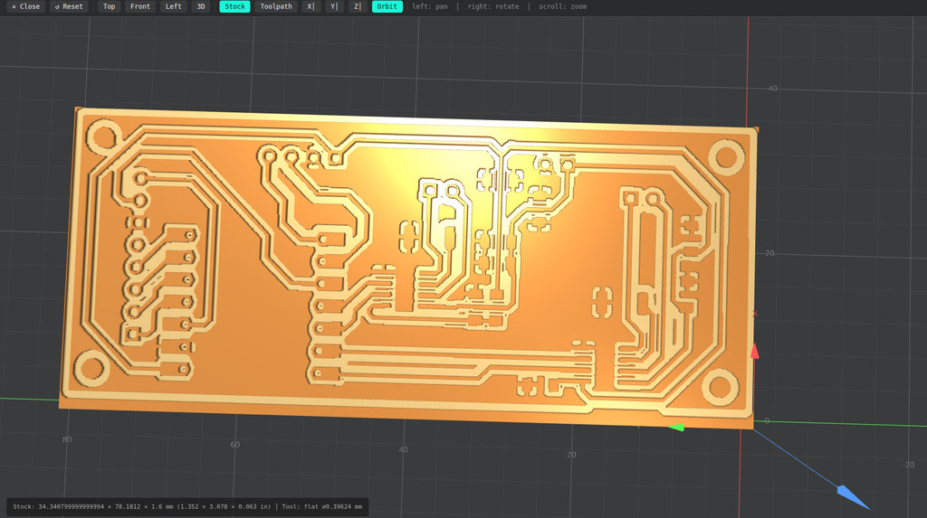
In the Set PCB Default section, I selected 1/64 flat when using inch units, or 1/64 flat end mill when using millimeters. In the Mill Raster 2D section, the parameters automatically updated based on the default settings, although they can also be adjusted manually. After that, I pressed Calculate, which immediately generated a 3D preview of the PCB design, where possible errors can be detected.
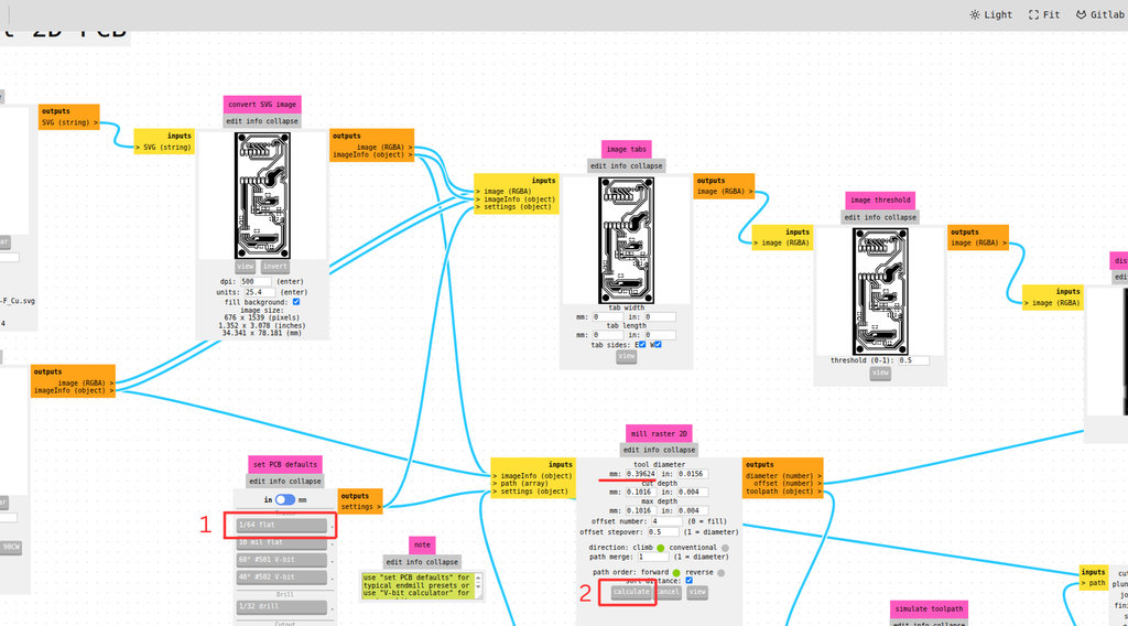
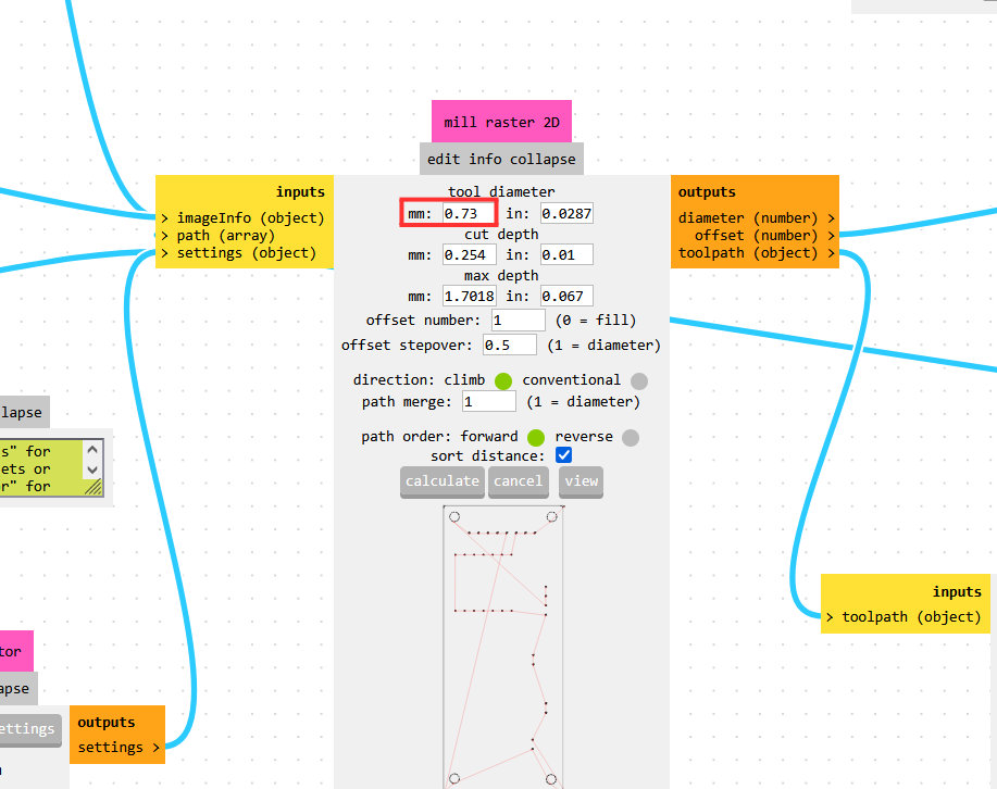
From the Mill Raster 2D section, I also clicked View to see the toolpath of the end mill, which helps identify any visible issues.
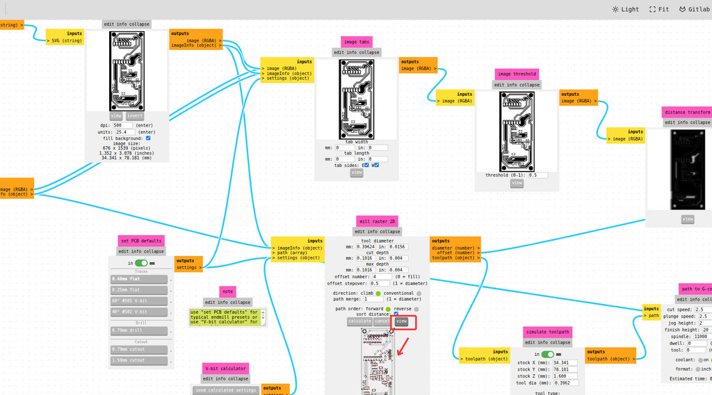
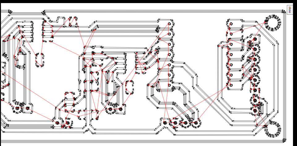
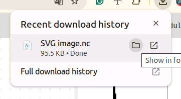
Since I did not notice any problems, I saved the file. For this, I enabled the On/Off checkbox and pressed Calculate again, which automatically downloaded the file in .nc format.
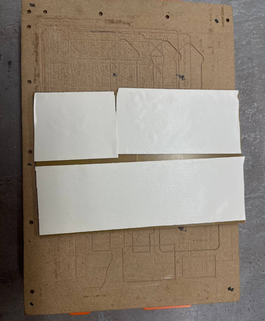
Since this PCB will still undergo many tests, and I also plan to redesign it to be more compact for the robot car and possibly adjust the size closer to the RC522 NFC reader module, I selected a scrap PCB area that was no longer usable but was large enough for the current design.
Next, the PCB piece had to be securely attached to the PCB Bed using double-sided tape, and I waited at least 5 minutes to ensure proper adhesion.
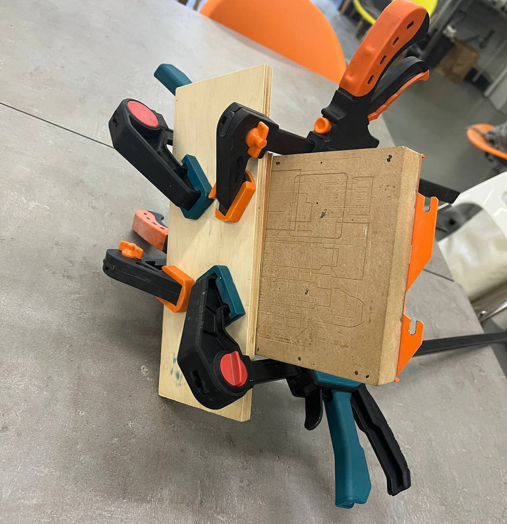
0.396748 mm milling bit, which corresponds to 1/64 inch.After that, I fixed the PCB Bed inside the monoFab SRM-20 using special CNC clamps. The PCB was machined using VCarve software. I slowly moved the end mill to the starting position where the engraving should begin and set the zero positions for X, Y, and Z axes.
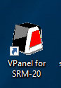
In the image above, you can see how I set the X and Y coordinates to zero. It is also necessary to zero the Z coordinate.
To do this, I gradually lower the Z-axis step by step, but not all the way until the end mill touches the PCB. I bring it as close as possible. Then I loosen the end mill and allow it to gently touch the PCB surface. After that, I tighten the end mill again and set the Z coordinate to 0.
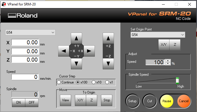
Once all coordinates are zeroed and the end mill is securely tightened, we are ready to proceed to the next step.
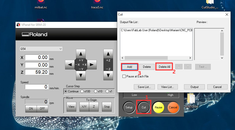
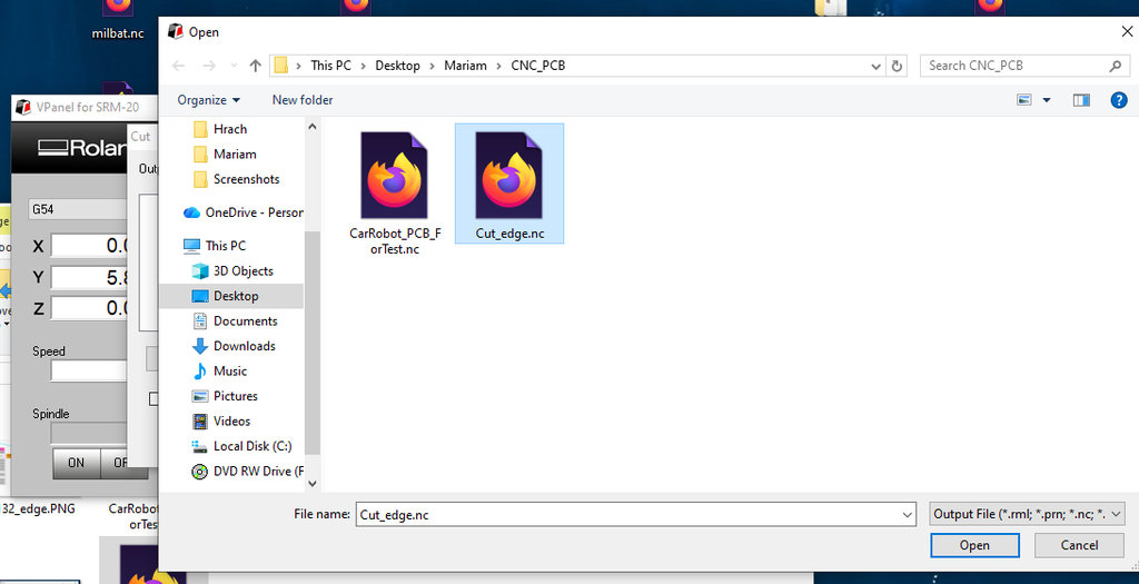
Then I pressed Cut, removed the previous file from the list, added my .nc file, and selected Output.
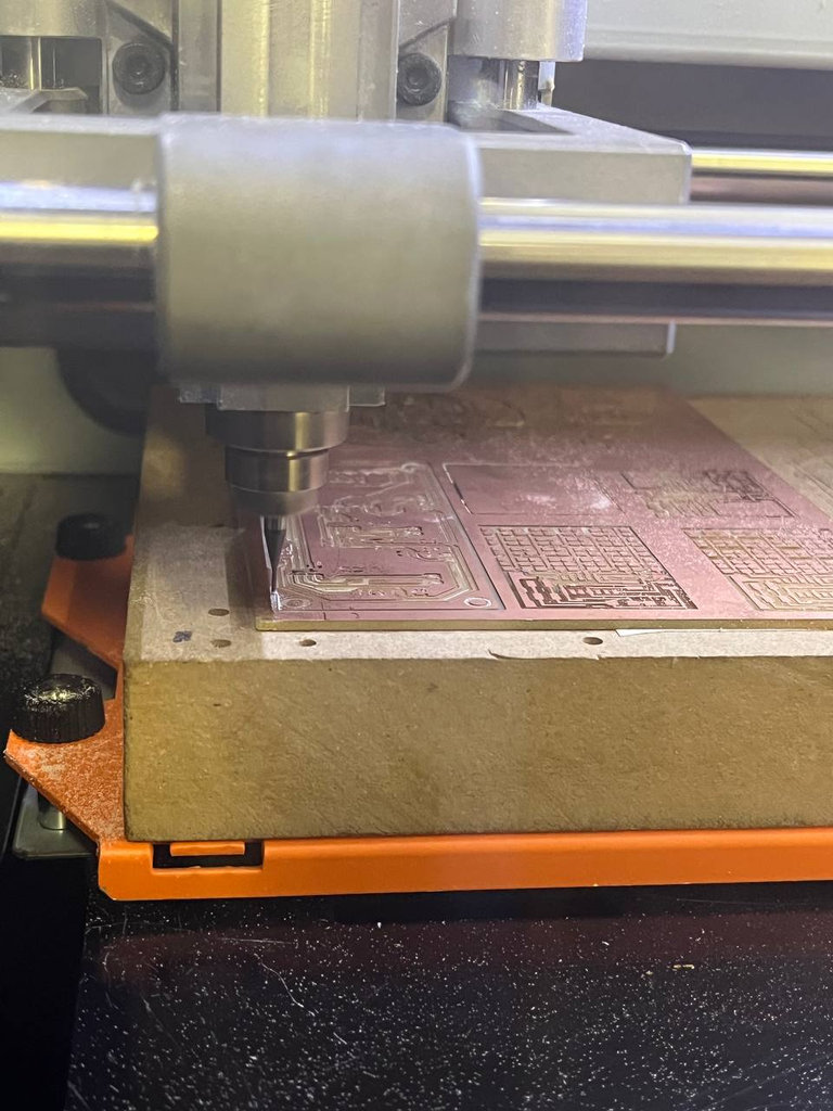
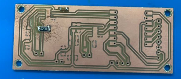
Here are some images from the machining process.
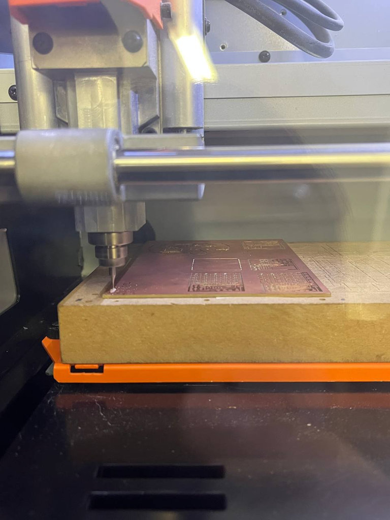
After the engraving finished, I carefully cleaned the dust using a vacuum cleaner without removing the PCB Bed, since I needed to change the milling bit to cut the edges.
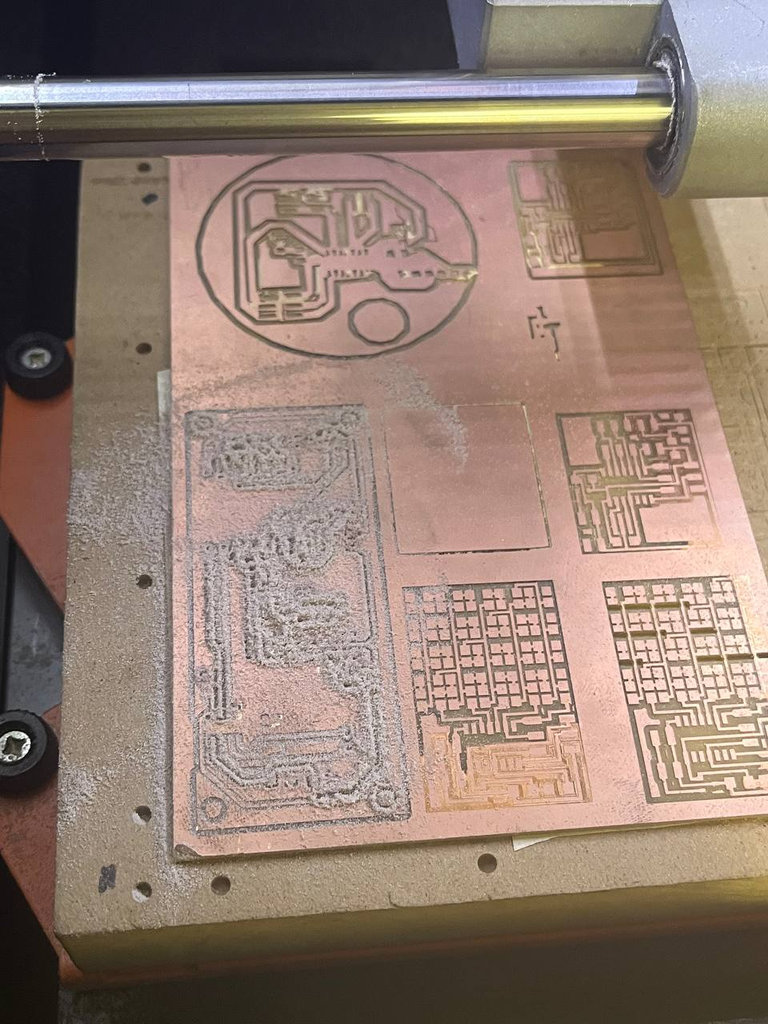
For the cutting operation, I selected a 1/32 inch milling bit, which is approximately 0.8 mm.
Next, I went again to modsproject.org. This time I selected Select SVG file and loaded the file corresponding to Edge.Cuts, which contains the outline of my PCB, including the edge holes and the holes for the pin headers.
Now, in the Set PCB Default section, I selected the 0.79 mm cutout milling bit from the Cutout options. After saving, I received an error message. This happened because the pin header holes are smaller than the 1/32 inch milling bit, so the machine could not drill them.
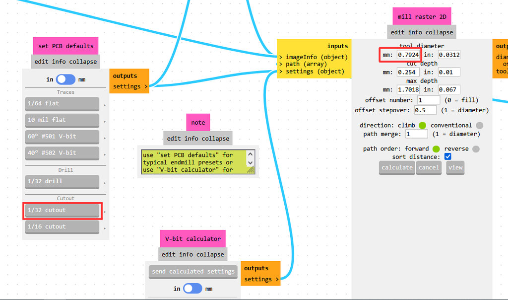
To solve this, I slightly adjusted the parameters by manually setting the tool diameter to 0.73 mm in the Mill Raster 2D section. This allowed the toolpath to generate correctly, since the program assumed the bit could fit into the holes. This workaround worked successfully.
After changing the milling bit, I needed to set the zero position again, but this time only for the Z axis. I found the correct Z position and reset it by pressing Zero Z.

Then I pressed Cut, removed the previous file, and loaded the new .nc file for the edge cutting process.
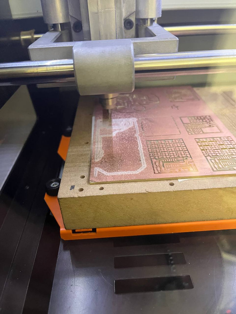
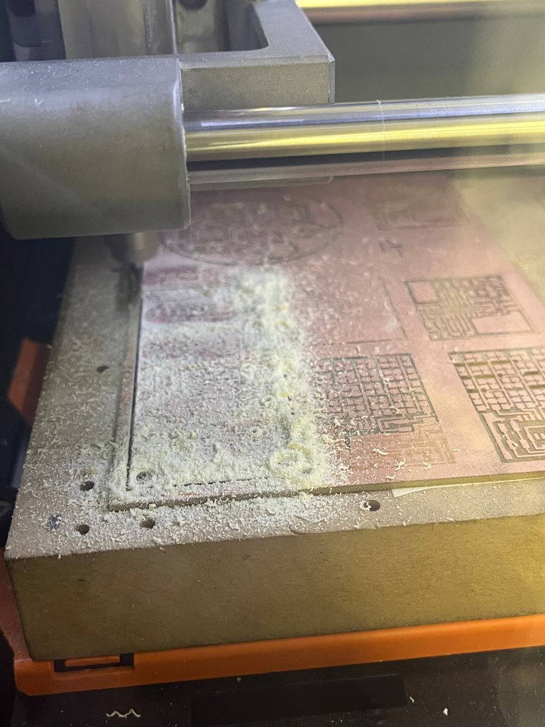
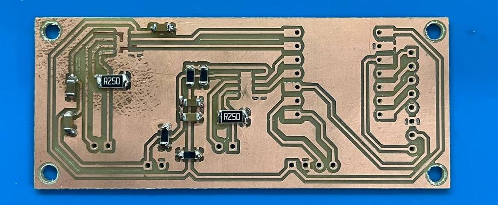
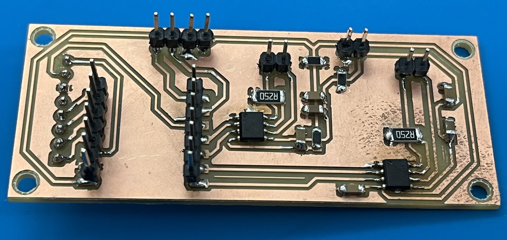
Here are some images from the cutting process.
PCB from the PCB bed.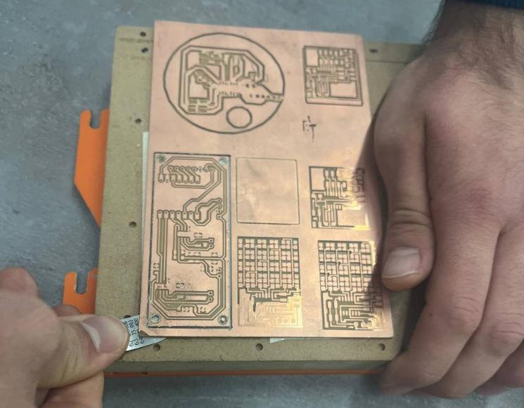
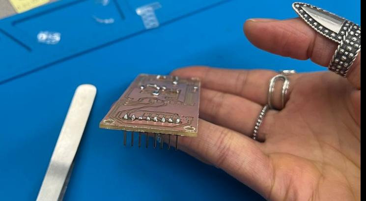
Finally, the moment I had been waiting for during the last 8 weeks arrived — soldering all the necessary components onto the PCB. I really enjoyed working in this electronics workspace.☺️
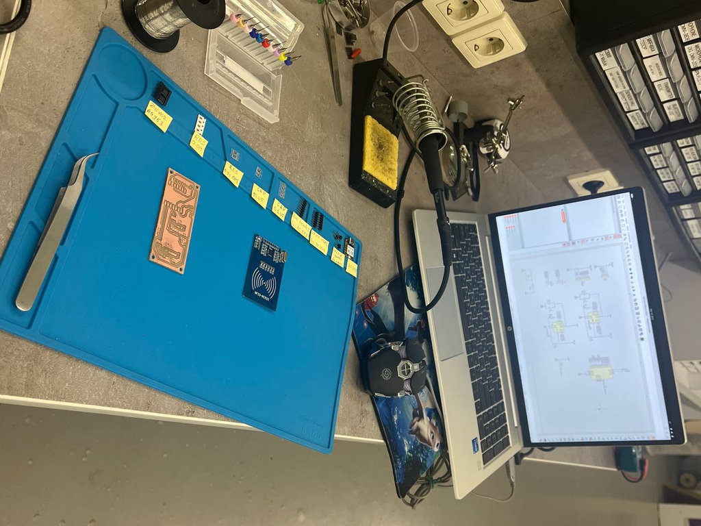
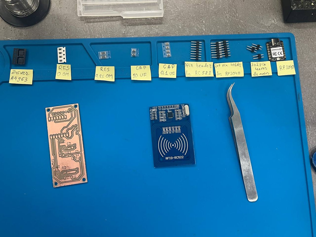
I collected all the components together and also made notes so I wouldn’t confuse them during the soldering process.
For soldering, I set my soldering iron to 350°C, which worked well for assembling all the SMD components on the PCB. This temperature provided a good balance between efficient soldering and avoiding excessive heat exposure to the components.
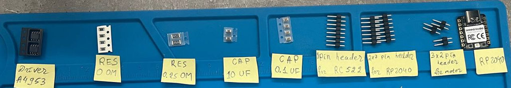
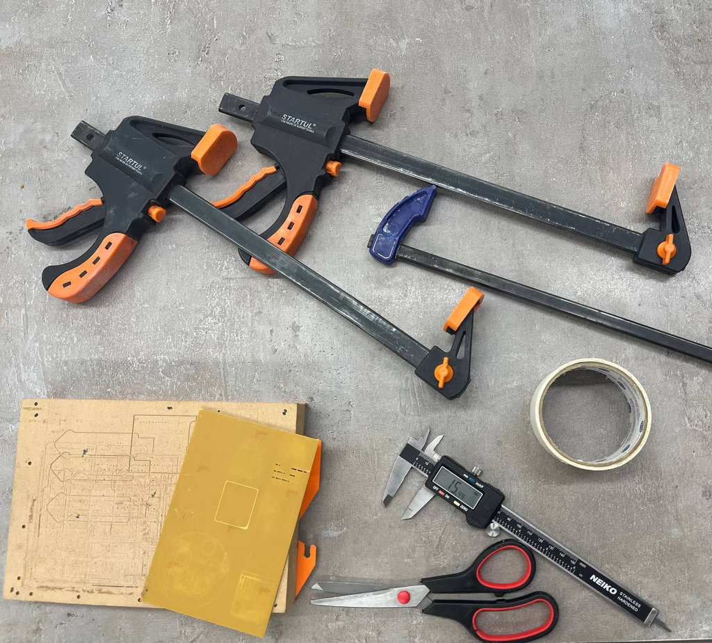
Tools and Equipment Used for Soldering
To assemble my PCB, I used the following tools and equipment:
- Temperature-controlled soldering station (set to
350°C) - Soldering iron
- Solder wire
- Flux
- Precision tweezers for placing SMD components
- Multimeter for continuity testing and debugging
- PCB holder / helping hands
- Side cutters for trimming component leads and pin headers
Here is the first soldered component 😍
Here is the second one 😍
And the process continued like this for the rest of the components.
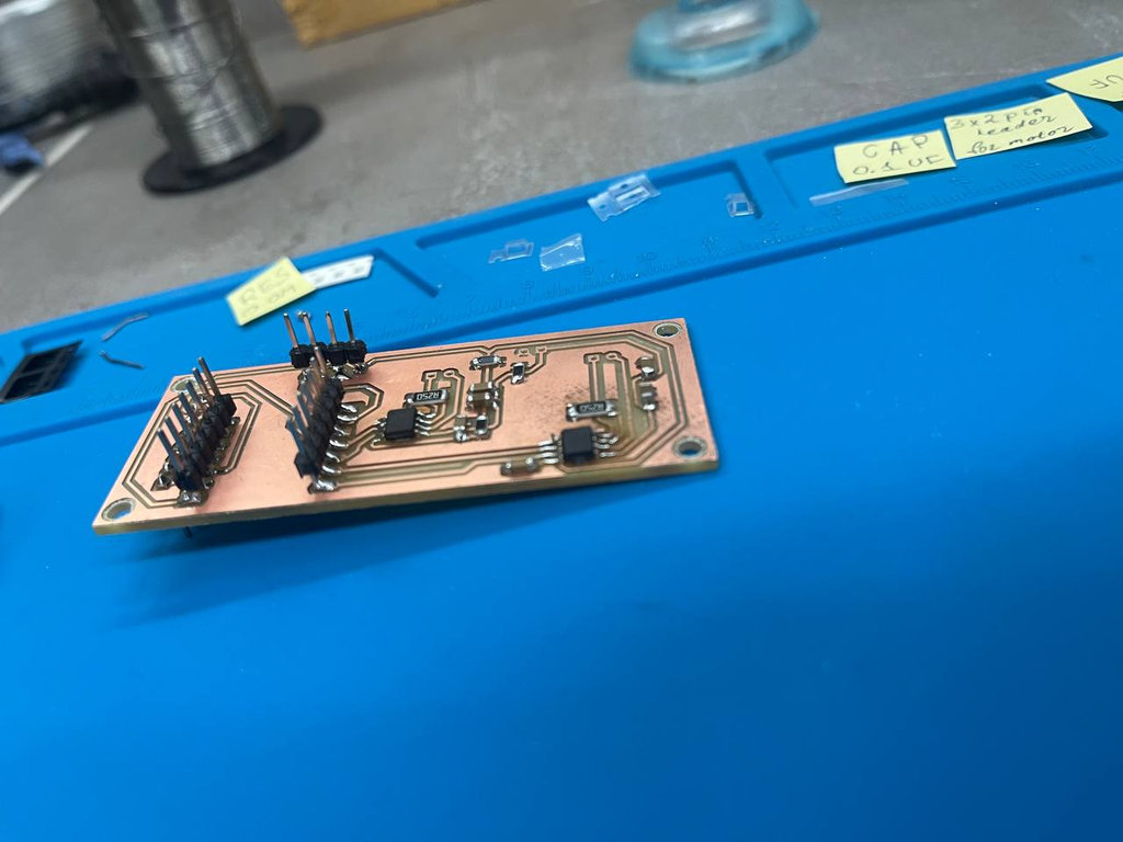
After that, to make sure everything was connected correctly and that there were proper contacts in the soldered areas, I tested all connections using a tester (multimeter).
During testing, I discovered that the GND of the RP2040 was not connected to the main GND. To fix this, I added a 0-ohm resistor in the appropriate place to bridge the connection.
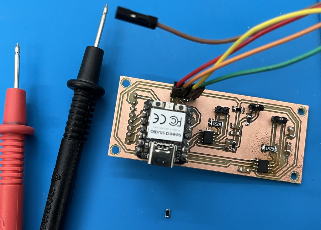
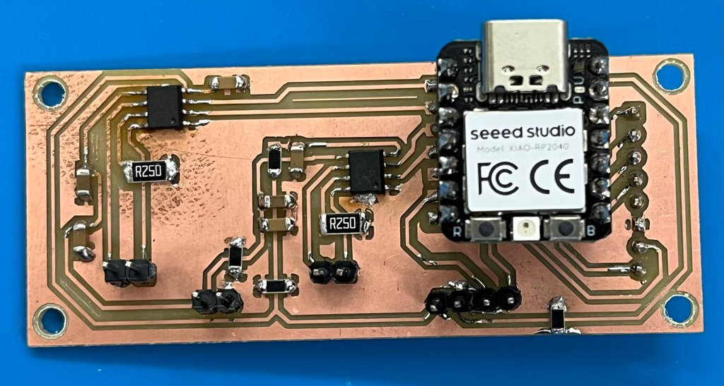
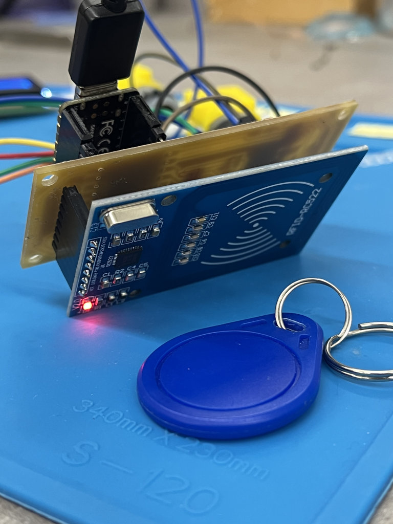
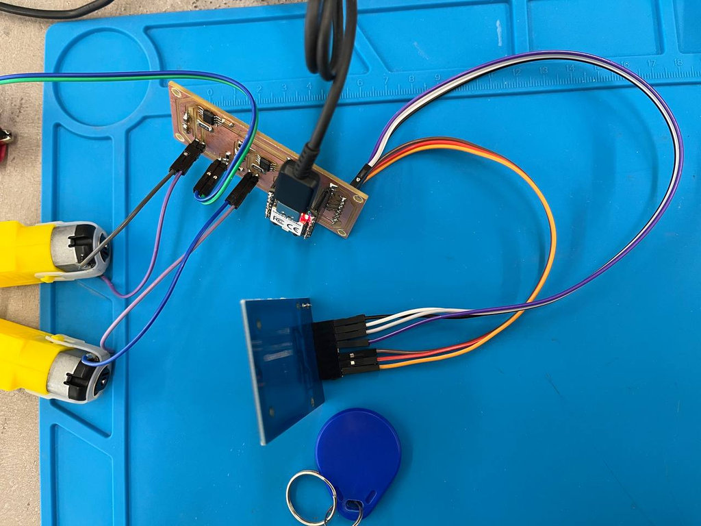
After checking the rest of the connections and confirming there were no further issues, I proceeded to the programming stage. I also mounted the RC522 module onto my PCB.
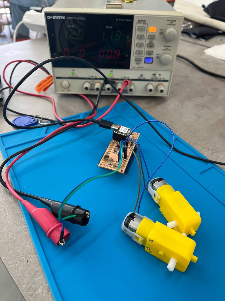
For testing purposes, I added a 2-pin connector header on my PCB to supply power at this stage using a power supply, providing 12V voltage to the board.
To save time and avoid spending too many hours writing the initial code, I asked my AI assistant:
"Write Arduino code for a Seeed Studio XIAO RP2040 using an H-bridge to control one DC motor."
After it generated the code, I modified it by adding the GPIO pins that I was using in my own PCB. At this stage, the program was designed to control only a single DC motor.
// XIAO RP2040 Pins
const int IN1 = D0;
const int IN2 = D1;

void setup() {
  pinMode(IN1, OUTPUT);
  pinMode(IN2, OUTPUT);

  // Ensure motor is off at start
  digitalWrite(IN1, LOW);
  digitalWrite(IN2, LOW);
}

void loop() {
  // Move Forward at 75% speed
  moveMotor(190, true);
  delay(2000);

  // Stop
  moveMotor(0, true);
  delay(1000);

  // Move Backward at 50% speed
  moveMotor(127, false);
  delay(2000);

  // Stop
  moveMotor(0, true);
  delay(1000);
}

void moveMotor(int speed, bool forward) {
  if (forward) {
    analogWrite(IN1, speed);
    digitalWrite(IN2, LOW);
  } else {
    digitalWrite(IN1, LOW);
    analogWrite(IN2, speed);
  }
}
Next, I expanded the code by implementing the logic required to control the second motor as well.
// Motor A (Driver 1)
const int MOT_A_IN1 = D0;
const int MOT_A_IN2 = D1;

// Motor B (Driver 2)
const int MOT_B_IN1 = D2;
const int MOT_B_IN2 = D3;

void setup() {
  pinMode(MOT_A_IN1, OUTPUT);
  pinMode(MOT_A_IN2, OUTPUT);
  pinMode(MOT_B_IN1, OUTPUT);
  pinMode(MOT_B_IN2, OUTPUT);

  // Initialize all pins to LOW (Stop)
  stopMotors();
}

void loop() {
  // Move both motors forward at 60% speed
  controlMotor(MOT_A_IN1, MOT_A_IN2, 150);
  controlMotor(MOT_B_IN1, MOT_B_IN2, 150);
  delay(2000);

  // Reverse both motors at 40% speed
  controlMotor(MOT_A_IN1, MOT_A_IN2, -100);
  controlMotor(MOT_B_IN1, MOT_B_IN2, -100);
  delay(2000);

  stopMotors();
  delay(2000);
}

// Function to control direction and speed
// Speed range: -255 (full reverse) to 255 (full forward)
void controlMotor(int pin1, int pin2, int speed) {
  if (speed > 0) { // Forward
    analogWrite(pin1, speed);
    digitalWrite(pin2, LOW);
  } else if (speed < 0) { // Reverse
    digitalWrite(pin1, LOW);
    analogWrite(pin2, abs(speed));
  } else { // Stop
    digitalWrite(pin1, LOW);
    digitalWrite(pin2, LOW);
  }
}

void stopMotors() {
  controlMotor(MOT_A_IN1, MOT_A_IN2, 0);
  controlMotor(MOT_B_IN1, MOT_B_IN2, 0);
}
Here is the result with both motors working.
I wrote a lot of code and struggled a lot to establish the connection between the NFC reader and NFC tag, but it wasn’t working. Maxim noticed that I had swapped the MISO and MOSI pins, and in my code, whenever I tried to assign them to different pins, it never worked because I hadn’t fully read the documentation. Thank you so much, Maxim jan, for spotting the mistake I had made.
To fix the problem, we connected the correct wires.
After that, I asked the AI to extend the code once more so that both motors would rotate continuously until the NFC reader detected an NFC tag. As soon as a tag was detected, the program would immediately stop both motors.
#include <Arduino.h>
#include <SPI.h>
#include <MFRC522.h>

// ----- RFID Setup -----
#define RST_PIN 6
#define SS_PIN 1
MFRC522 rc(SS_PIN, RST_PIN);

// ----- Motor Pins -----
const int MOT_A_IN1 = D0;
const int MOT_A_IN2 = D1;
const int MOT_B_IN1 = D2;
const int MOT_B_IN2 = D3;

// ----- Motor Control -----
int motorState = 1; // 1 = forward, 2 = reverse, 0 = stop
unsigned long motorTimer = 0;
const unsigned long MOTOR_INTERVAL = 2000; // 2 seconds per action
int motorSpeedForward = 150;
int motorSpeedReverse = 100;

void setup() {
  Serial.begin(9600);

  // Motor pins
  pinMode(MOT_A_IN1, OUTPUT);
  pinMode(MOT_A_IN2, OUTPUT);
  pinMode(MOT_B_IN1, OUTPUT);
  pinMode(MOT_B_IN2, OUTPUT);
  stopMotors();

  // Initialize SPI and MFRC522
  SPI.begin();
  rc.PCD_Init();
  Serial.println(F("Ready to read tags..."));
  motorTimer = millis(); // start timer
}

void loop() {
  // ----- Check RFID -----
  bool tagPresent = rc.PICC_IsNewCardPresent() && rc.PICC_ReadCardSerial();
  if (tagPresent) {
    Serial.println(F("Tag detected! Stopping motors."));
    stopMotors();
    return; // Skip motor actions
  }

  // ----- Motor control -----
  unsigned long currentTime = millis();
  if (currentTime - motorTimer >= MOTOR_INTERVAL) {
    motorTimer = currentTime;

    // Cycle motor state
    motorState++;
    if (motorState > 2) motorState = 1;
  }

  // Run motors according to state
  if (motorState == 1) { // Forward
    controlMotor(MOT_A_IN1, MOT_A_IN2, motorSpeedForward);
    controlMotor(MOT_B_IN1, MOT_B_IN2, motorSpeedForward);
  } else if (motorState == 2) { // Reverse
    controlMotor(MOT_A_IN1, MOT_A_IN2, -motorSpeedReverse);
    controlMotor(MOT_B_IN1, MOT_B_IN2, -motorSpeedReverse);
  }
}

// ----- Motor Functions -----
void controlMotor(int pin1, int pin2, int speed) {
  if (speed > 0) { // Forward
    analogWrite(pin1, speed);
    digitalWrite(pin2, LOW);
  } else if (speed < 0) { // Reverse
    digitalWrite(pin1, LOW);
    analogWrite(pin2, abs(speed));
  } else { // Stop
    digitalWrite(pin1, LOW);
    digitalWrite(pin2, LOW);
  }
}

void stopMotors() {
  controlMotor(MOT_A_IN1, MOT_A_IN2, 0);
  controlMotor(MOT_B_IN1, MOT_B_IN2, 0);
}
Here is the final result:
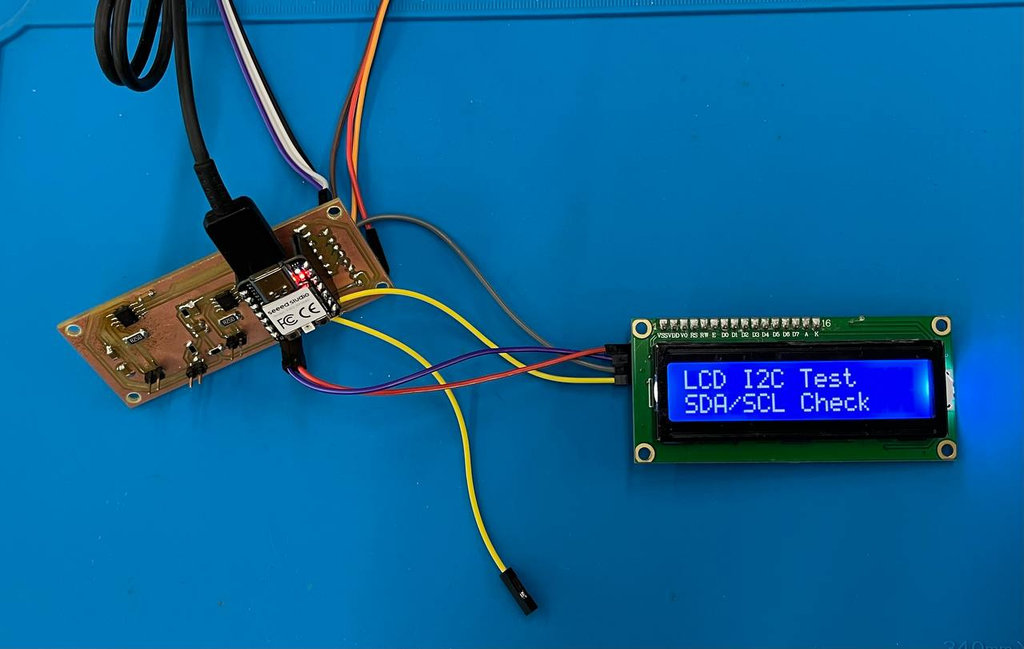
To make sure that the connections related to the LCD were correct (since I had already tested them with the multimeter), I wrote a simple program just to print text.
However, the text was not appearing at all. After carefully reviewing the pins, I realized that testing alone was not enough — I needed to properly read the documentation and use the correct RP2040 pins that are compatible with the component.
To fix this issue and finally see text on the LCD, I connected the correct pins using wires and printed the text using the following code.
#include <LiquidCrystal_PCF8574.h>>

// Replace 0x27 with the address you find from the scanner
LiquidCrystal_PCF8574 lcd(0x27);

void setup() {
  Serial.begin(9600);
  delay(2000);

  Serial.println("LCD I2C Test Starting...");

  Wire.begin();  // default SDA/SCL pins of RP2040

  lcd.begin(16, 2);     // 16x2 LCD
  lcd.setBacklight(255); // turn on backlight

  // Test printing
  lcd.setCursor(0, 0);
  lcd.print("Test  LCD I2C Test");

delay(1000);


  lcd.setCursor(0, 1);
  lcd.print("SDA/SCL Check");
}

void loop() {
  // Nothing here
}
During Week 8, I learned how to manufacture and assemble a PCB, starting from milling and ending with soldering and testing. I worked with CNC PCB cutting, generated toolpaths, and understood how different milling bits affect the final result. I also practiced soldering components and testing connections using a multimeter, which helped me identify and fix issues like missing GND connections.
I really liked the hands-on part, especially soldering and seeing the PCB come to life as a working system. It was exciting to finally assemble something I designed myself.
The most boring part for me was the long preparation process, such as setting parameters, generating files, and waiting during machining. However, I understand that these steps are important for achieving accurate results.
Overall, this week helped me gain practical skills in PCB production, debugging, and hardware integration.
Individual assignment
AI prompt:
“And when she finished week 8 and motors is worked and also nfs tag is works fine”